

Page 1
LOVE TESTER KIT
MODEL AK-500/K-39
Assembly and Instruction Manual
ElencoTMElectronics, Inc.
Copyright © 1994 ElencoTMElectronics, Inc. Revised 2003 REV-D 753239
Page 2
PARTS LIST
Contact ElencoTMElectronics (address/phone/e-mail is at the back of this manual) if any parts are missing or
damaged. DO NOT contact your place of purchase as they will not be able to help you.
RESISTORS
Qty. Symbol Value Color Code Part #
2 R1, R8 470W 5% 1/4W yellow-violet-brown-gold 134700
1 R5 15kW 5% 1/4W brown-green-orange-gold 151500
1 R2 56kW 5% 1/4W green-blue-orange-gold 155600
1 R7 68kW 5% 1/4W blue-gray-orange-gold 156800
1 R3 100kW 5% 1/4W brown-black-yellow-gold 161000
1 R4, R6 1.5MW 5% 1/4W brown-green-green-gold 171500
CAPACITORS
Qty. Symbol Value Description Part #
1 C1 .0039mF (392) Mylar 233917
1 C2 .015mF (153) Mylar 241517
1 C3 2.2mF 50V Electrolytic (Lytic) 262247
1 C4 47mF 16V Electrolytic (Lytic) 274744
SEMICONDUCTORS
Qty. Symbol Value Description Part #
1 D1 1N4148 Diode 314148
1 Q1 2N3904 Transistor 323904
1 U1 4011 Integrated Circuit (IC) 334011
1 U2 4017 Integrated Circuit (IC) 334017
8 LED 1 - 8 Light Emitting Diode (LED) 350001
MISCELLANEOUS
Qty. Description Part #
1 PC Board 517017
1 Dimple Switch 546101
1 Battery Snap 590098
1 Buzzer Piezoelectric 595201
1 Filter Red 621425
1 Spacer 7/32” 624008
PARTS IDENTIFICATION
Resistor
Diode
Battery Snap
Capacitors
Electrolytic
Mylar
Qty. Description Part #
1 Tape 2-sided 1” 748127
1 Cushion Tape 1” 790006
1 Wire Red 22ga. 1” 814220
1 Wire Bare 24ga. 1” 835000
1 Solder Tube 9ST4
Switch
Dimple
Buzzer
Integrated Circuit
IC Socket
LED
Transistor
-1-
Page 3
IDENTIFYING RESISTOR VALUES
Use the following information as a guide in properly identifying the value of resistors.
Bands
1 2
Multiplier
Tolerance
BAND 1
1st Digit
Color Digit
Black 0
Brown 1
Red 2
Orange 3
Yellow 4
Green 5
Blue 6
Violet 7
Gray 8
White 9
BAND 2
2nd Digit
Color Digit
Black 0
Brown 1
Red 2
Orange 3
Yellow 4
Green 5
Blue 6
Violet 7
Gray 8
White 9
Multiplier
Color Multiplier
Black 1
Brown 10
Red 100
Orange 1,000
Yellow 10,000
Green 100,000
Blue 1,000,000
Silver 0.01
Gold 0.1
Resistance
Tolerance
Color Tolerance
Silver +10%
Gold +
Brown +1%
Red +2%
Orange +
Green +.5%
Blue +.25%
Violet +
5%
3%
.1%
IDENTIFYING CAPACITOR VALUES
Capacitors will be identified by their capacitance value in pF (picofarads), nF (nanofarads), or mF (microfarads).
Most capacitors will have their actual value printed on them. Some capacitors may have their value printed in the
following manner.
Second Digit
First Digit
Multiplier
Tolerance
Multiplier
The above value is 10 x 1,000 = 10,000pF or .01mF
The letter K indicates a tolerance of +
10%
The letter J indicates a tolerance of +5%
For the No.01234589
Multiply By 1 10 100 1k 10k 100k .01 0.1
Note: The letter “R” may be used at times to
signify a decimal point; as in 3R3 = 3.3
INTRODUCTION
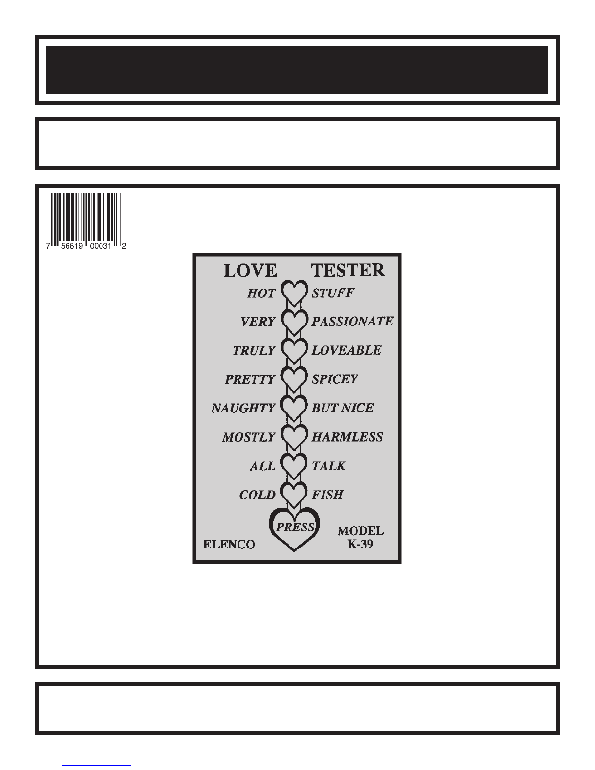
Want to know what kind of lover you are? Push the PRESS button and the Love Tester will rate you as a
lover. The Love Tester has eight Light Emitting Diodes (LEDs) that are driven ON and OFF one at a time
in sequence. When the PRESS button is pushed, the LEDs will flash and the buzzer will sound. After a
brief period of time, only one LED will remain lit. Above the lit LED is your rating as a lover, anywhere from
Cold Fish to Hot Stuff. In a minute or two, the LED will get dim and gradually go out.
THEORY OF OPERATION
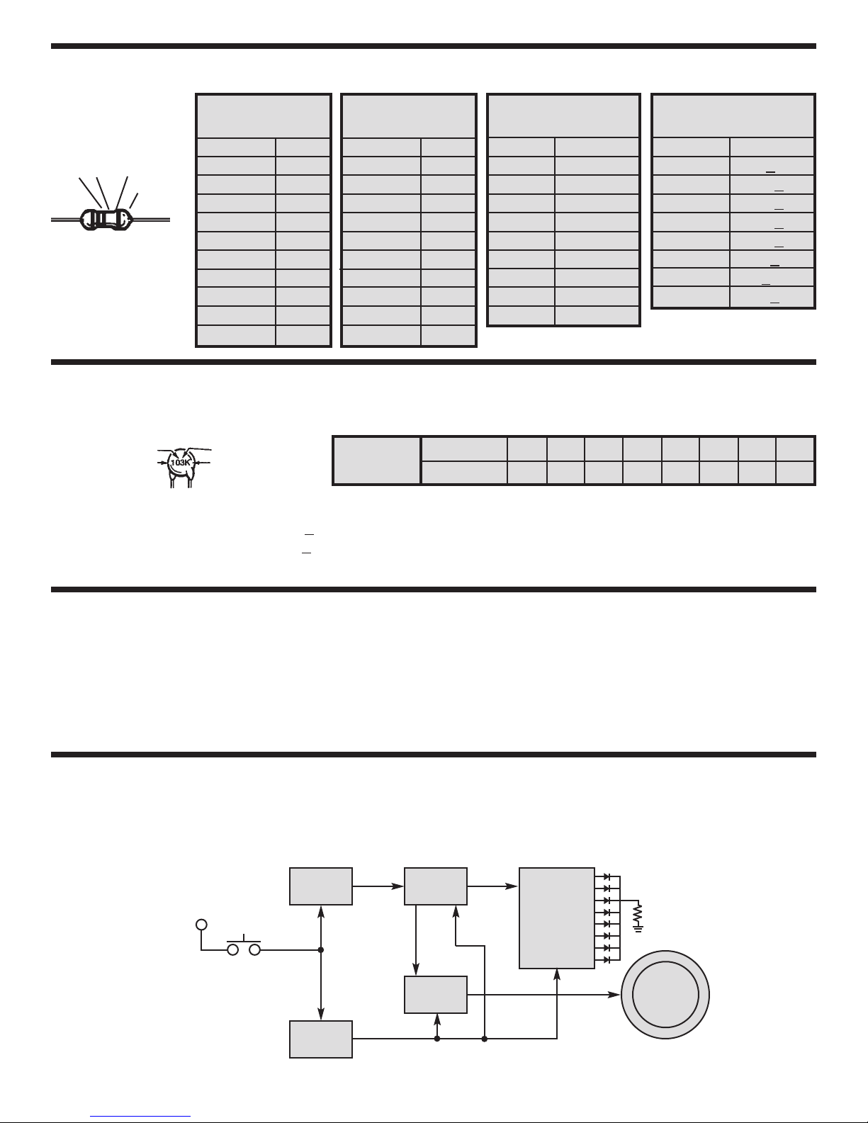
Figure 1 shows the block diagram of the Love Tester circuit. It consists of two oscillators and eight LEDs driven
by a decade counter. One oscillator drives the decade counter and the oscillators are controlled by two timers.
We shall proceed to study the circuit in detail.
LEDs
Figure 1
B+
BUTTON
PRESS
Timer 1
OSC 1
Decade
Counter
OSC 2
Timer 2
Buzzer
-2-
Page 4
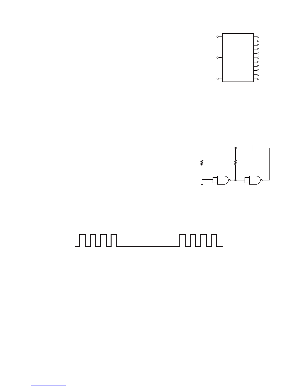
THE DECADE COUNTER
The 4017 IC is a 5 stage divide by 10 counter. Figure 2 shows a diagram of this IC. This
IC has 10 outputs and a clear input. Only one of the 10 outputs will be high at any given
time. The other 9 will be low. Let’s assume that output 1 is high. If a pulse is fed into the
clock input, output 1 will go low and output 2 will go high. Each clock pulse will move the
output one position. Connect an LED to the output, it will light only when the output goes
high. It is obvious that when the clock is running, the LEDs will flash on and off with the
speed of the clock. When the clock stops, only one LED will be lit.
In this design, 8 LEDs are used per IC, but the counter has 10 outputs. If the clock stops
at an output without an LED, nothing will light. To prevent this, the 4017 IC is reset after
hitting the 8th output. This is simply done by tying the 9th output to the clear pin (pin 9
and pin 15 shorted together).
Block Diagram
14
1
15
Clock
Clock
Enable
Reset
Q0
Q1
Q2
Q3
Q4
Q5
Q6
Q7
Q8
Q9
OUT
C
VDD - Pin 16
VSS - Pin 8
3
2
4
7
10
1
5
6
9
11
12
THE LIGHT EMITTING DIODES (LED)
Figure 2
The operation of the LED is very simple. When current flows through the LED, it will emit
light. Note that the LED is connected between an IC output and ground through a resistor. When the IC output goes high,
the LED will light. The resistor limits the current so that the LED will not be damaged.
OSCILLATORS
The Love Tester uses two oscillators. The first oscillator produces a frequency of about 20 hertz (cycles) and the other
produces a frequency of about 2000 hertz. Figure 3 shows the basic oscillator
circuit. The 4011 integrated circuit (IC) contains four two-input NAND gates. Two
of these NAND gates are needed to form an oscillator. Feed back for this
oscillator is via capacitor C2 and resistors R4 and R5. These elements
R5
determine the frequency of oscillation. Both IC1 and IC2 act as inverters, that
is, when the input is low, the output is high. As long as pin 13 of IC1 is high, the
circuit will oscillate. If pin 13 is brought low, the circuit will stop oscillating.
The second oscillator is similar to the one described except for a difference in its
frequency controlling components, capacitor C1 and resistors R2 and R3. C1
Pin 13
+V
IC1
4011 IC
Figure 3
and R2 are smaller values causing the oscillator to oscillate at a much higher frequency. Pin 6 of the first NAND gate is
brought high at a 20 cycles rate. This causes the second oscillation to be chopped up at the first oscillation frequency rate
as shown in Figure 4. This combination produces the unusual sound heard from the buzzer.
C2
R4
IC2
BUZZER
The Love Tester buzzer consists of a piezoelectric material on a metal base. When a voltage is applied to piezoelectric
material, its dimensions change. The buzzer is connected to the 2kHz oscillator. When the oscillator runs, the changing
dimensions to the piezoelectric buzzer act like the cone of a speaker to set up sound waves.
TIMER
Timer 1 is made up of capacitor C3 and R6. Timer 2 is made up of capacitor C4 and R7 (see schematic diagram). When
S1 is pushed, both capacitors charge up to 9 volts and the oscillators run. When the switch is released, capacitor C3
discharges through resistor R6 and capacitor C4 discharges through resistor R7 and the base of Q1.
Note that C3 is tied to pin 13 of the 4011 IC. Thus, when capacitor C3 loses its charge, the circuit stops oscillating. The
buzzer stops and a single LED remains lit. After a minute or two, C4 loses its charge and removes the base current from
Q1. Q1 is in the ground return path of the LEDs and both ICs. Thus, when Q1 is turned off, the LED goes out. Only a very
small leakage current is then drawn from the battery. This current is so small that no ON/OFF switch is required.
Figure 4
-3-
Page 5

CONSTRUCTION
Introduction
The most important factor in assembling your AK-500 Love Tester Kit is good soldering techniques. Using the
proper soldering iron is of prime importance. A small pencil type soldering iron of 25 - 40 watts is
recommended. The tip of the iron must be kept clean at all times and well tinned.
Safety Procedures
• Wear eye protection when soldering.
Locate soldering iron in an area where you do not have to go around it or reach over it.
•
• Do not hold solder in your mouth. Solder contains lead and is a toxic substance. Wash your hands
thoroughly after handling solder.
• Be sure that there is adequate ventilation present.
Assemble Components
In all of the following assembly steps, the components must be installed on the top side of the PC board unless
otherwise indicated. The top legend shows where each component goes. The leads pass through the
corresponding holes in the board and are soldered on the foil side.
Use only rosin core solder of 63/37 alloy.
DO NOT USE ACID CORE SOLDER!
What Good Soldering Looks Like
A good solder connection should be bright, shiny,
smooth, and uniformly flowed over all surfaces.
1. Solder all components from
the copper foil side only.
Push the soldering iron tip
against both the lead and
the circuit board foil.
2. Apply a small amount of
solder to the iron tip. This
allows the heat to leave the
iron and onto the foil.
Immediately apply solder to
the opposite side of the
connection, away from the
iron. Allow the heated
component and the circuit
foil to melt the solder.
3. Allow the solder to flow
around the connection.
Then, remove the solder
and the iron and let the
connection cool. The
solder should have flowed
smoothly and not lump
around the wire lead.
4.
Here is what a good solder
connection looks like.
Component Lead
Foil
Solder
Foil
Solder
Foil
Soldering Iron
Circuit Board
Soldering Iron
Soldering Iron
Types of Poor Soldering Connections
1. Insufficient heat - the
solder will not flow onto the
lead as shown.
2. Insufficient solder - let the
solder flow over the
connection until it is
covered. Use just enough
solder to cover the
connection.
3. Excessive solder - could
make connections that you
did not intend to between
adjacent foil areas or
terminals.
4. Solder bridges - occur
when solder runs between
circuit paths and creates a
short circuit. This is usually
caused by using too much
solder. To correct this,
simply drag your soldering
iron across the solder
bridge as shown.
Rosin
Soldering iron positioned
incorrectly.
Solder
Component Lead
Solder
Soldering Iron
Foil
Gap
Drag
-4-
Page 6

ASSEMBLE COMPONENTS TO THE PC BOARD
Black
Red
J3 & J4 - Battery Snap
Install the red wire into the positive (+) hole
and the black wire into the negative (–)
hole as shown. Bend the leads to hold the
battery snap in place. Solder and cut off
the excess leads.
LED 5 - Light Emitting Diode
(see Figure A)
LED 4 - Light Emitting Diode
(see Figure A)
LED 8 - Light Emitting Diode
(see Figure A)
LED 7 - Light Emitting Diode
(see Figure A)
LED 3 - Light Emitting Diode
(see Figure A)
U2 - 4017 Integrated Circuit
(see Figure B)
LED 1 - Light Emitting Diode
(see Figure A)
LED 2 - Light Emitting Diode
(see Figure A)
LED 6 - Light Emitting Diode
(see Figure A)
R7 - 68kW 5% 1/4W Resistor
(blue-gray-orange-gold)
Q1 - 2N3904 Transistor
(see Figure C)
C3 - 2.2mF 50V Electrolytic
(see Figure D)
R6 - 1.5MW 5% 1/4W Resistor
(brown-green-green-gold)
C4 - 47mF 16V Electrolytic
(see Figure D)
D1 - 1N4148 Diode
(see Figure E)
JP1 - Jumper Wire
(see Figure F)
C1 - .0039mF (392) Mylar Cap.
(see Figure G)
R2 - 56kW 5% 1/4W Resistor
(green-blue-orange-gold)
R1 - 470W 5% 1/4W Resistor
(yellow-violet-brown-gold)
R3 - 100kW 5% 1/4W Resistor
(brown-black-yellow-gold)
U1 - 4011 Integrated Circuit
(see Figure B)
R5 - 15kW 5% 1/4W Resistor
(brown-green-orange-gold)
R4 - 1.5MW 5% 1/4W Resistor
(brown-green-green-gold)
Figure A
Mount the LED
flush to the PC
board with the flat
side of the LED in
the same direction
as marked on the
PC board.
Flat
Mount the transistor with the flat
side in the same direction marked
on the PC board. Leave about
1/16” space between the PC board
and the transistor.
Figure B
Insert the IC into the PC board
with the notch in the same
direction as marked on the PC
board.
Notch
Electrolytic capacitors have polarity. Be
sure to mount them with the negative (–)
lead (marked on side) in the correct hole.
Mount the electrolytics horizontal to the
PC board. Bend the leads at right angles
and then insert the leads into the PC
board.
Figure C
Flat
Figure D
Figure E
Diodes have polarity.
Mount them with the
band in the correct
direction, as shown on
the PC board.
Band
Polarity
Marking
-5-
C2 - .015mF (153) Mylar Cap.
(see Figure G)
R8 - 470W 5% 1/4W Resistor
(yellow-violet-brown-gold)
Figure F
Form a discarded piece of a capacitor lead long
enough so 1/4” of wire passes through each hole in
the PC board. Mount the wire down close.
Figure G
Mount the mylar capacitor to the PC
board and bend it 90Oas shown. Solder
and cut off the excess leads.
Page 7

ASSEMBLE COMPONENTS TO THE PC BOARD (CONTINUED)
Figure I
Solder the 1” 24 ga. bare wire to S1 and S2 as shown. Cut the wire so
that each end extends 1/16” above the PC board. Then, bend the wires
toward each other and also press them flat against the PC board with
your pliers. Place the dimple switch with the dome upward over the S1
and S2 wires. Hold the switch in place with the double-sided tape.
Mount the spacer on top of the switch, the double-sided tape on the
switch will hold it in place.
Tape
Dimple
Switch
Mount the buzzer on the foil side of the PC board. The white
center should be facing up, also note the position of the pad in
the white area. Solder the buzzer to the PC board at the two
points. Strip the insulation off of both ends of the red wire to
expose 1/8” of bare wire. Solder the wire to the buzzer and PC
board.
BZ1
Figure H
Solder Points
Cut the cushion tape into four equal 1/4” sections. Peel off the protective film on one side of the tape and stick
a section of tape on each corner of the PC board on the top legend side (see Figure J). Place the spacer
over the dimple switch as shown in Figure J. Peel off the protective film on the other side of the tape and stick
the red filter in place so that the “press” heart is directly over the spacer on the switch (see Figure J).
Red Filter
1/4” Cushion Tape
PC Board
1/4” Cushion Tape
Spacer
-6-
Page 8

OPERATING PROCEDURE
Operating your Love Tester is very simple. Just connect a 9 volt battery to the battery snap and you are ready
to go. Push the PRESS button to get your rating as a lover!
TROUBLESHOOTING
Contact ElencoTMElectronics if you have any problems. DO NOT contact your place of purchase as they will not
be able to help you.
1. One of the most frequently occurring problems is poor solder connections.
a) Tug slightly on all parts to make sure that they are indeed soldered.
b) All solder connections should be shiny. Resolder any that are not.
c) Solder should flow into a smooth puddle rather than a round ball. Resolder any connection that has formed into a ball.
d) Have any solder bridges formed? A solder bridge may occur if you accidentally touch an adjacent foil by using too much solder
or by dragging the soldering iron across adjacent foils. Break the bridge with your soldering iron.
2. Be sure that all components have been mounted in their correct places.
a) The LEDs will not light if they have not been installed correctly. The flat side of the LEDs should be in the same direction as
marked on the PC board.
b) Be sure capacitors C3 and C4 are installed correctly. These capacitors are polarized so be sure that the positive and negative
leads are in the correct hole as marked on the PC board.
c) Be sure that ICs U1 and U2 are installed correctly. The notch should be in the direction shown on the PC board.
d) Be sure that transistor Q1 has been installed correctly. The flat side of the transisor should be in the same direction as marked
on the PC board.
e) Be sure that diode D1 is installed correctly. The stripe on the diode should be in the same direction as the stripe marked on
the PC board.
3. Use a fresh 9 volt ALKALINE battery.
4. NO SOUND AND NO LEDs
a) Check that the battery snap is wired as shown on page 5 of this manual. The black wire goes to J4 (–) and the red wire goes
to J3 (+).
b) Check that U1 and U2 are not installed backwards. Be sure that there are no solder bridges between the IC pins.
c) Check that the dimple switch is mounted with the dome upward.
d) Check the value and the soldering of R7.
e) Check Q1.
5. CONTINUOUS SOUND AND LED
a) Check the wires in S1 and S2. They should make contact with the dimple switch only when the “PRESS” heart on the red filter
is pressed.
6. LEDs BUT NO SOUND
a) Check that the buzzer is soldered as shown in Figure D on page 5. Check that the solder connection between the jumper wire
and the center pad of the buzzer.
b) Check for soldering bridges between the pins of U1.
c) Check the value and the soldering of R1, R2, and R3.
7. LEDs STOP AS SOON AS THE SWITCH IS RELEASED
a) Check that C3 and C4 are mounted with the negative (–) lead in the hole marked on the PC board.
b) Check the value and soldering of R6.
c) Check D1.
-7-
Page 9

QUIZ
Fill in the blanks and check your answers below.
1. When driven by clock pulses, the outputs of the decade counter will go on and _____________ at a time in
sequence.
2. LEDs are driven by a _____________ _____________.
3. The 4017 IC contains a _________ stage divide by _____________ counter.
4. The Love Tester uses _____________ oscillators.
5. The 4011 IC contains four two input _____________ gates.
6. When a voltage is applied to the piezoelectric buzzer, it changes its _____________.
7. When the PRESS button is pushed, capacitors C3 and C4 charge up to 9V, and the _____________ start
running.
8. After the oscillators stop, only one LED will remain lit and then gradually fade out as _____________ loses
its charge.
Foil Side of PC Board
Answers: 1. off; 2. decade counter; 3. five, ten; 4. two; 5. NAND; 6. dimension; 7. oscillators; 8. C4
-8-
Page 10

SCHEMATIC DIAGRAM
-9-
Page 11

NOTES
-10-
Page 12

ElencoTMElectronics, Inc.
150 W. Carpenter Avenue
Wheeling, IL 60090
(847) 541-3800
http://www.elenco.com
e-mail: elenco@elenco.com
 Loading...