

AC/DC POWER SUPPLY KIT
MODEL K-11
Assembly and Instruction Manual
Elenco®Electronics, Inc.
ight © 2004, 1989 b
yr
Cop
t of this book shall be reproduced b
No par
y Elenco
®
Electronics
y means;
y an
, Inc.
electronic
ights reser
All r
, photocopying, or otherwise without written permission from the publisher.
ved. Revised 2004 REV-J 753211

PARTS LIST
If you are a student, and any parts are missing or damaged, please see instructor or bookstore.
If you purchased this AC/DC power supply kit from a distributor, catalog, etc., please contact Elenco
(address/phone/e-mail is at the back of this manual) for additional assistance, if needed. DO NOT contact your
place of purchase as they will not be able to help you.
RESISTORS
Qty. Symbol Value Color Code Part #
1 R1 1kΩ 5% 1/4W brown-black-red-gold 141000
1 R3 2.7kΩ 5% 1/4W red-violet-red-gold 142700
1 R2 10kΩ Potentiometer 191516
CAPACITORS
Qty. Symbol Value Description Part #
1 C2 100µF Electrolytic 281045
1 C1 1000µF Electrolytic 291045
SEMICONDUCTORS
Qty. Symbol Value Description Part #
2 D1, D2
1 D3 1N5247 Zener Diode 315247
1 Q1 2N3904 Transistor 323904
1 Q2 2N6121 / HT1061
1N4001 Diode
Transistor
®
Electronics
314001
326121
MISCELLANEOUS
Qty. Symbol Description Part #
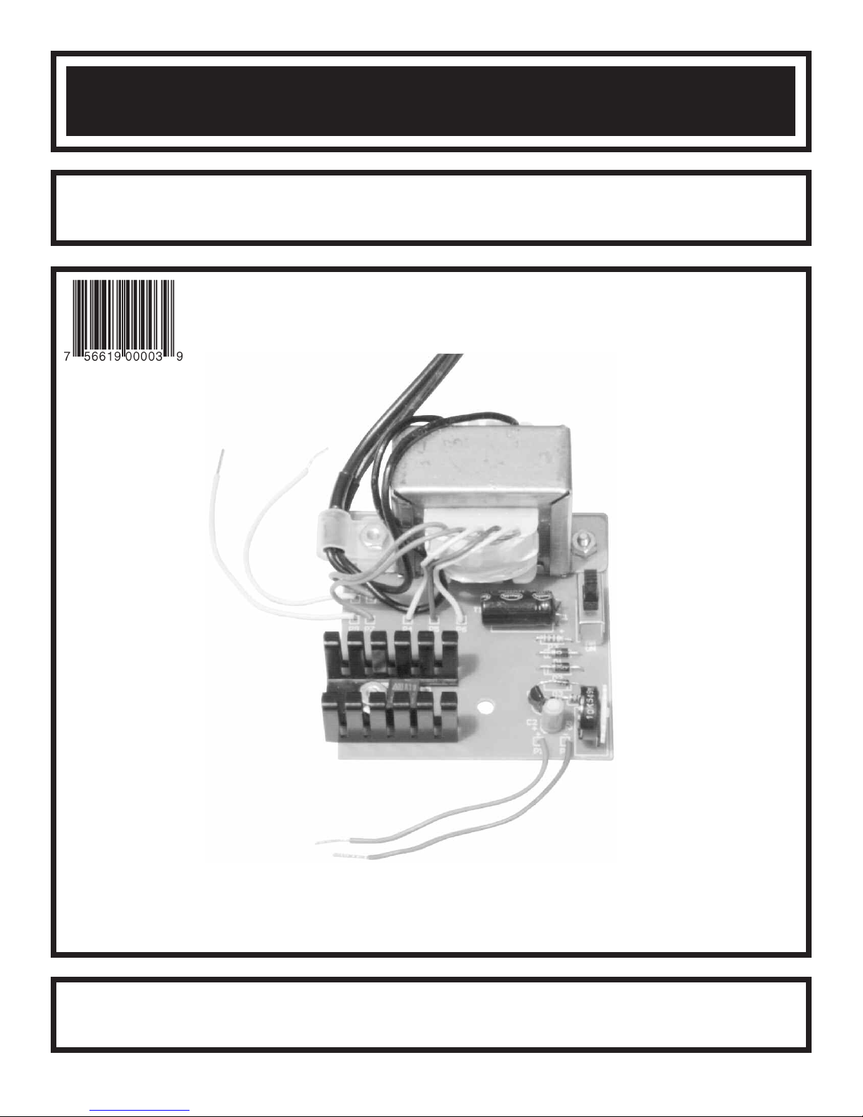
1 T1 Transformer YD-1485 440111
1 PC Board 518011
1 S1 Slide Switch 541009
1 Solder Roll
551124
1 Heat Sink 615002
1 Cable Clamp 1/4” 628750
3 Scre
w 6-32 x 5/16” 641641
3 Nut 6-32 644600
1 Line Cord 862100
1 Shrink Tubing 2” 890120
PARTS IDENTIFICATION
ransformer
Resistor Transistors
EBC
Diode
BCE
Cable
Clamp
Capacitor
Potentiometer
Switch
T
Heat Sink
Epoxy
Glass
Electrolytic
-1-

INTRODUCTION
The electrical power that is supplied by your power
company is what is known as Alternating Current or
AC. This current is constantly changing amplitude and
polarity (see Figure 1). The electrons (current) move
back and forth at a rate of 60 times per second. This
type of current is not suitable for most electronic
circuits. It must be converted into a Direct Current or
DC which moves in one direction only. Your MultiPurpose Power Supply does exactly that. It converts
THEORY OF OPERATION
A block diagram of the system is shown in Figure 2. It
consists of five basic circuits needed to convert 120
volts of AC to a usable 0-15 volts of DC. We will
analyze each circuit for a better understanding of
power supplies.
13VAC
Voltage
Stepdown
Voltage and
Current Control
0-15V
Output
Figure 2
VOLTAGE STEP-DOWN FUNCTION
In this circuit, 120 volts of AC is
reduced to two 13VAC out of
phase v
the rms (eff
peak voltage is really 18 v
This step-down is achieved by
the use of a transformer. The
winding of the transformer is
shown in Figure 3A and the
voltage across each winding is
shown in Figure 3B. In a
transformer, the magnetic field
produced b
current is induced into the
secondar
across the secondary winding is a ratio of the number
of turns between the primary and secondary winding.
If the r
voltage would be the same as the 120 volt input. In our
tr
secondary voltage will be 13 volts. If we were to put
an oscilloscope betw
secondary windings and looked at the other leads, we
would see that the two voltages are 180 degrees out
of phase
opposite directions from the common point. This is an
impor
see in the next section.
oltages. Thirteen v
ective) value. The
y the 120 v
y winding. The voltage
atio was 1:1 (equal turns), then the secondary
ansf
or
mer
, the r
atio is 120:13.
een the common lead of the two
This is because the windings are going in
.
er
tant point in con
v
Rectification
AC to DC
Filtering
Reference
Voltage
olts is
olts.
olts of
ting the A
DC
120VAC
AC Peak
AC Peak
Figure 3A
18V
–18V
Figure 3B
Therefore, the
C to DC as w
18V
–18V
36Vpp
36Vpp
e will
AC into DC. It also
allows you to vary the
amplitude of the
voltage from 0-15V
(0.25A - 12Vmax).
Also, your power
supply has an output
+168V
or
–168V
Time
336V
Peak to
Peak (PP)
or 120V
rms
of 8.5VAC, 0.5A
without regulation.
Figure 1
AC to DC CONVERSION - RECTIFICATION
This circuit that converts AC to
DC consists of two diodes D1
and D2. The purpose of a
diode is to pass current in only
one direction (see Figure 4). If
we were to take a battery and
connect it to a diode and lamp,
Direction of
Current Flow
Figure 4
as shown in Figure 5, the lamp would only light when
the diode is in the conduction direction. If we replace
the battery with a transformer secondary winding, the
diode will only conduct on the positive cycle of the
voltage as shown in Figure 6.
Note that the output of
the diode is a half-wave rectification with a hole in the
center. This voltage would be hard to filter out. It is
desirable to fill in this area. This is done by something
known as full wave rectification, which is using a
second winding out of phase with the first.
Battery
Diode
ot Lit
N
Lamp
Diode
Resistor
Figure 6
Diode
Battery
Lamp
Figure 5
Figure 7A shows the circuit for a full wave rectification.
Note that diode D1 conducts the previously described
and diode D2, one half cycle later. The diodes conduct
only when the voltage goes positive and no current
. The resulting output voltage
ws on the negativ
flo
e half
waveforms are shown in Figure 7B. Note that there is
no longer a gap betw
een cycles. This will make it
easier to filter the output voltage.
D1
Figure 7A
D2
Output D1
Figure 7B
Output D2
D1 & D2
-2-

FILTERING
Filtering is the process of
smoothing out AC hills
produced by the full wave
rectifiers. The circuit consists of
the 1000µF capacitor C1. A
capacitor is an electrical device
Battery
that stores electrical energy. If
two metal plates are placed
very close to each other and
are connected to a battery, a
current will flow momentarily,
Figure 8A
Radial
Axial
even though there is no
connection between the plates
Figure 8B
(see Figure 8A). If the battery
is removed, a voltage will remain on the plates. These
plates are now charged and will act like a battery.
Current can be drawn from this capacitor until the
charge is consumed. Typical capacitors are shown in
Figure 8B.
The capability of storing a charge on a capacitor is
measured in farads (F). Most capacitors used in
electronic power supplies are rated in microfarads (µF)
which means one millionth of a far
ad. Typical values
are 100 to 10,000µF. Capacitors used in power
supplies are called electrolytics because of their
design. An electrolytic is used in a power supply to
smooth out the rectified A
C voltages. During the peak
voltage, energy is supplied to the capacitor and
released during the valleys between the peaks (see
Figure 9). The current through the diode will initially be
very high until the electrolytic is charged. Then, little
bursts of current are
needed to supply the
current going to the load.
Remember, current will
Voltage without
Capacitor
Voltage with
Capacitor
18VP
only flow through the
diode when the driving
Current in
Diode
voltage is greater than
the DC across the
Figure 9
electrolytic.
REFERENCE VOLTAGE
An impor
tant element of a w
ell regulated po
is a dependable reference voltage. This gives a stable
oltage which does not vary with the load current. The
v
component used to make this voltage in Elenco’s
supply is called a z
In our discussion of diodes
ener diode (D3).
e talk
, w
flow in one direction, but none when we reverse the
oltage. If, in the reverse direction, we keep increasing
v
the voltage, the diode will breakdown and current will
eventually flow. This breakdown is called zener
. Manufacturers have learned to control this
oltage
v
breakdown voltage and supply zener diodes for almost
wer supply
ed about current
any voltage. Figure 10 shows the zener circuit used in
our power supply. The DC filter output voltage will vary
between 18 minimum and a higher voltage, depending
on load current. The voltage across the zener diode
will remain constant at 17V. This constant voltage is
important to
control the
output of the
regulators as
you will see in
the following
Filtered Output
Voltage at C1
18V min.
R1
Figure 10
17V
D8
Reference
Voltage
section.
VOLTAGE REGULATOR
Figure 11A shows the circuit of the voltage regulator.
It consists of two transistors and a variable resistor.
Our objective is to control the output of Q1 to give the
desired voltage of 0-15 volts. This output should not
change with different loads.
To understand the circuit operations, we must have a
little knowledge of transistors. Br
iefly, the voltage at
the emitter (Figure 11B) of a transistor will be .7V less
than the voltage on the base. If we put 10 volts on the
base, then 9.3 volts will appear on the emitter. The
emitter voltage will stay fixed, even though the
collector v
oltage may vary. Thus, increasing or
decreasing the collector voltage will not effect the
emitter voltage, providing the base voltage stays fixed.
If we increase the load on the transistor, more current
will flow. This increased current will produce a drop in
the filter DC voltage across the electrolytic, but the
zener diode will hold the reference fixed and thus the
output voltage of Q1 will be constant. This process is
called Regulation. A good regulator will not change
the output voltage with load current changes.
To vary the output voltage of transistor Q1, we place a
variable resistor R2 to divide the output from the zener
diode. Thus, we can vary the 17 volt zener output
between 0-17 volts and control Q1’s output. Transistor
Q2 is used to reduce the current drawn from the zener
circuit.
Filtered
Volts min.
17
TM
Zener
Res. Volt
Q1
Variable
Resistor
Q2
Load
R2
Figure 11A
Collector
Base
Emitter
Figure 11B
-3-

CONSTRUCTION
Introduction
The most important factor in assembling your K-11 Power Supply Kit is good soldering techniques. Using the
proper soldering iron is of prime importance. A small pencil type soldering iron of 25 - 40 watts is
recommended. The tip of the iron must be kept clean at all times and well tinned.
Safety Procedures
• Wear eye protection when soldering.
Locate soldering iron in an area where you do not have to go around it or reach over it.
•
• Do not hold solder in your mouth. Solder contains lead and is a toxic substance. Wash your hands
thoroughly after handling solder.
• Be sure that there is adequate ventilation present.
Assemble Components
In all of the following assembly steps, the components must be installed on the top side of the PC board unless
otherwise indicated. The top legend shows where each component goes. The leads pass through the
corresponding holes in the board and are soldered on the foil side.
Use only rosin core solder of 63/37 alloy.
DO NOT USE ACID CORE SOLDER!
What Good Soldering Looks Like
A good solder connection should be bright, shiny,
smooth, and uniformly flowed over all surfaces.
1. Solder all components from
the copper foil side only.
Push the soldering iron tip
against both the lead and
the circuit board foil.
2. Apply a small amount of
solder to the iron tip. This
allows the heat to leave the
iron and onto the f
Immediately apply solder to
the opposite side of the
connection, away from the
iron. Allow the heated
component and the circuit
oil to melt the solder.
f
Allow the solder to flo
3.
around the connection.
Then, remove the solder
and the iron and let the
connection cool.
solder should have flowed
smoothly and not lump
around the wire lead.
4.
Here is what a good solder
connection looks like.
oil.
The
Component Lead
Foil
Solder
Foil
w
Solder
F
oil
Soldering Iron
Circuit Board
Soldering Iron
Soldering Iron
Types of Poor Soldering Connections
1. Insufficient heat - the
solder will not flow onto the
lead as shown.
2. Insufficient solder - let the
solder flow over the
connection until it is
vered. Use just enough
co
solder to co
connection.
3. Excessive solder - could
make connections that you
did not intend to between
adjacent foil areas or
minals.
ter
4. Solder bridges - occur
when solder runs between
circuit paths and creates a
short circuit. This is usually
caused by using too much
solder. To correct this,
simply dr
iron across the solder
bridge as shown.
ag y
ver the
our solder
ing
Rosin
Soldering iron positioned
incorrectly.
Solder
Component Lead
Solder
Solder
Foil
ing Iron
Dr
Gap
ag
-4-

ASSEMBLE COMPONENTS TO THE PC BOARD
1 - Transformer, two 6-32 x
T
5/16” Screws, two 6-32 Nuts,
Shrink Tubing, Cable Clamp, &
Line Cord
C
ut the shrink tubing into two 1” sections.
Slip a section of tubing onto each of the
two lead wires on the line cord.
Twist each of the two wires on the line
cord with the two black wires from the
transformer. Solder these wires.
Slide the shrink tubing down over both
black wires to cover the solder joints.
Doing this will prevent a shock hazard.
Keeping your soldering iron close, but
not touching, let the heat from the iron
shrink the tubing.
Using two screws, two nuts and a cable
clamp, install the transformer onto the
PC board.
Cut a 3” section off of each of the red,
yellow, and blue transformer leads.
They will be used later. Strip 1/4” off of
the leads.
Solder the two yellow, two red and one
blue lead from the transformer to the
pads of the PC board as shown.
P8 - 3” yellow wire *
P9 - 3” yellow wire *
Q2 - 2N6121/HT1061 Transistor
Heat Sink
6-32 x 5/16” Screw
6-32 Nut
(see Figure A)
* Strip 1/4” of insulation off of both ends of the wire.
Figure A
Bend the leads of the transistor in the direction
shown below.
Install the transistor with the heat sink onto the
component side of the PC board using the
screw and nut as shown. Solder the leads of
the transistor and cut off the excess leads.
1/16”
Bend leads 90
O
1” Shrink Tubing
Red Wire
Blue Wire
Figure B
Diodes have polarity. Mount them
with the band in the correct direction,
as shown on the PC board.
Line Cord
Black
Transformer
Wires
Red Transformer Wires
Yellow Transformer Wire
Blue Transformer Wire
Yellow Transformer Wire
C1 - 1000µF Electrolytic Cap.
(see Figure C)
(Mount Horizontally)
S1 - Slide Switch
R3 - 2.7kΩ 5% 1/4W Resistor
(red-violet-red-gold)
D1 - 1N4001 Diode
D2 - 1N4001 Diode
(see Figure B)
D3 - 1N5247 Zener Diode
(see Figure B)
R1 - 1kΩ 5% 1/4W Resistor
(brown-black-red-gold)
R2 - 10kΩ Potentiometer
Q1 - 2N3904 Transistor
(see Figure D)
C2 - 100µF Electrolytic Cap.
(see Figure C)
(Mount Vertically)
P2 - 3” Blue Wire *
P1 - 3” Red
Wire *
6-32 Nut
PC Board
2N6121/HT1061
ansistor
r
T
Heat sink
6-32 X 5/16”
Screw
Figure C
Electrolytic capacitors have polarity.
Be sure to mount them with the
e (–) lead (mar
negativ
the correct hole. Bend the capacitor
wn.
as sho
Polarity
king
Mar
1/8”
ed on side) in
k
-5-
Figure D
Mount the transistor with the flat side in
the same direction as shown on the PC
Solder and cut off the excess
board.
leads.
Flat
1/4”
EBC

OPERATING PROCEDURE
To operate the K-11 Power Supply, plug the line cord into a 120V, 60Hz AC outlet, turn the switch (S1) to the
ON position and rotate the potentiometer (R2) to make the output voltage climb from 0 to 15 volts DC. The red
wire from P1 is the positive output, the blue wire from P2 is the negative DC output, and the two yellow wires
are the AC output - 8.5V without regulation.
utput AC
O
Positive
DC: 0-15V @ 250mA
Output DC
Negative
AC: 8.5V @ 500mA
TROUBLESHOOTING
One of the most frequently occurring problems is poor solder connections.
1. Tug slightly on all parts to make sure that they are indeed soldered.
2. All solder connections should be shiny. Resolder any that are not.
Solder should flow into a smooth puddle rather than a round ball. Resolder any connection that has formed
3.
into a ball.
Have any solder bridges formed? A solder bridge may occur if you accidentally touch an adjacent foil by
4.
using too much solder or by dragging the soldering iron across adjacent foils. Break the bridge with your
soldering iron.
OUTPUT
COMPONENT CHECK
1. Be sure that all components have been mounted in their correct places.
2. Be sure that the electrolytic capacitors C1 and C2 have been installed correctly. These capacitors have
polarity, the negative and positive leads must be in the correct holes.
3. Be sure that diodes D1 - D3 have not been installed backwards. The band on the diodes should be in the
same direction as shown in the pictorial diagram.
SCHEMATIC DIAGRAM
-6-

QUIZ
M
ark the box next to the letter with the correct answer.
1.
AC voltage is supplied to the rectifier stages by
the . . .
A. step-up transformer.
B. step-down transformer.
C. 1-to-1 transformer.
D. AC-to-DC transformer.
2.
The secondary windings of the transformer are . . .
A. 90Oout of phase.
B. 180Oout of phase.
C. 270Oout of phase.
D. 320
3. Diodes allow current to flow . . .
A. when the anode is more negative than the
B. when the cathode is more positive than the
C. in one direction.
D. when a negative or positive voltage is on the
4.
What circuit is more efficient for rectifying AC to
DC?
A. Hartley oscillator.
B. Half-w
C. Schmitt trigger.
D. Full wave.
The DC v
5.
A. half-wave rectification circuit.
B. small value capacitor with a high voltage
C. Large value capacitor.
D. 90
O
out of phase.
cathode.
anode
anode
.
.
alf.
oltage is filtered by using a .
value.
O
out of phase rectification circuit.
. .
6.
An inefficient rectification circuit usually contains . . .
A. large gaps between cycles.
B. twice the AC voltage needed.
C. more diodes.
D. all of the above.
7. The ratio of the transformer in the K11 is . . .
A. 50:1.
B. 1:10.
C. 120:13.
D. 60:120.
8. The voltage at the emitter of a transistor is . . .
A. 0.7 volts less than the base.
B. 2 volts higher than the collector.
C. same as the collector.
D. 1.25 volts lower than the base.
9. A good regulator circuit . . .
A. changes the output under load.
B. contains many transistors
.
C. will not change under load.
D. uses small capacitors.
10. Transistor Q2 is used to . . .
oltage.
A. rectify the A
C v
B. filter the DC voltage.
C. amplify the AC voltage.
D. reduce the current dr
aw from the zener.
Elenco®Electronics, Inc.
150 Carpenter Avenue
Wheeling, IL 60090
(847) 541-3800
Website: www.elenco.com
e-mail: elenco@elenco.com
Answers: 1. B; 2. B; 3. C; 4. D; 5. C; 6. D; 7. C; 8. A; 9. C; 10. D
 Loading...