

Page 1

AUTO-SCAN FM RADIO KIT
MODEL FM-88K
Assembly and Instruction Manual
ELENCO
®
Copyright © 2011 by ELENCO®All rights reserved. 753050
No part of this book shall be reproduced by any means; electronic, photocopying, or otherwise without written permission from the publisher.
ELENCO
®
150 Carpenter Avenue
Wheeling, IL 60090
(847) 541-3800
Website: www.elenco.com
e-mail: elenco@elenco.com
To see our complete line of Educational Products
go to WWW.ELENCO.COM
Page 2

-14-
-1-
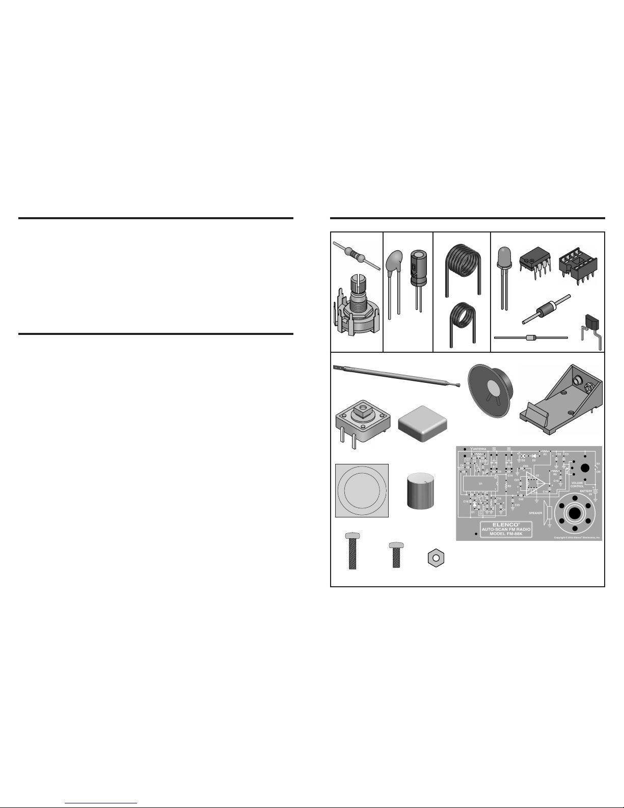
PARTS LIST
If you are a student, and any parts are missing or damaged, please see instructor or bookstore. If you purchased this
kit from a distributor, catalog, etc., please contact ELENCO
®
(address/phone/e-mail is at the back of this manual) for
additional assistance, if needed. DO NOT contact your place of purchase as they will not be able to help you.
RESISTORS
Qty. Symbol Value Color Code Part #
r 1 R5 10Ω 5% 1/4W brown-black-black-gold 121000
r 1 R1 680Ω 5% 1/4W blue-gray-brown-gold 136800
r 1 R3 5.6kΩ 5% 1/4W green-blue-red-gold 145600
r 1 R4 10kΩ 5% 1/4W brown-black-orange-gold 151000
r 1 R2 18kΩ 5% 1/4W brown-gray-orange-gold 151800
r 1 R6/S3 Potentiometer 50kΩ & switch w/ nut & washer 192522
CAPACITORS
Qty. Symbol Value Description Part #
r 1 C6 33pF Discap (33) 213317
r 1 C7 82pF Discap (82) 218210
r 1 C10 180pF Discap (181 or 180) 221810
r 1 C5 220pF Discap (221 or 220) 222210
r 1 C8 330pF Discap (331 or 330) 223317
r 1 C4 470pF Discap (471 or 470) 224717
r 1 C13 680pF Discap (681 or 680) 226880
r 1 C23 1500pF Discap (152) 231516
r 2 C11, C12 3300pF Discap (332) 233310
r 1 C15 0.033μF Discap (333) 243318
r 1 C19 0.047μF Discap (473) 244780
r 6 C3, C9, C14, C16, C17, C* 0.1μF Discap (104) 251010
r 2 C21, C22 10μF Electrolytic radial 271044
r 1 C20 22μF Electrolytic radial 272244
r 1 C1 100μF Electrolytic radial 281044
r 2 C2, C18 220μF Electrolytic radial 282244
COILS
Qty. Symbol Value Description Part #
r 1 L2 Coil 4-turn 430150
r 1 L1 Coil 6-turn 430160
SEMICONDUCTORS
Qty. Symbol Value Description Part #
r 1 D1 BB909/BB910 Varactor 310909
r 1 D2 1N4001 Semiconductor silicon diode 314001
r 1 D3 Red LED 3mm 350003
r 1 U2 LM-386 or identical Low voltage audio power amplifier 330386
r 1 U1 TDA7088T or identical FM receiver SM installed on PC board
MISCELLANEOUS
Qty. Description Part #
r 1 Antenna FM 484005
r 1
PC board w/ installed U1 (TDA7088T)
517038
r 2 Push button switch 12mm 540005
r 1 Battery holder 590096
r 1 Speaker 8Ω 590102
r 1 Cap push button switch yellow 622001
r 1 Cap push button switch red 622007
r 1 Knob pot / switch 622050
Qty. Description Part #
r 1 Screw M1.8 x 7.5mm 641100
r 2 Antenna screw M2 x 5mm 643148
r 1 Nut M1.8 644210
r 1 Socket IC 8-pin 664008
r 1 Speaker pad 780128
r 3” Wire 22 ga. solid 834012
r 1 Solder Lead-free 9LF99
RF Radio Frequency.
Sensitivity The ability of a receiver to pick
up low-amplitude signals.
Speaker An electronic device that turn
electric impulses into sound.
Surface-mount A method of using special
Technology components that are soldered
to the PC board’s surface.
Trimmer An adjustable fine-tuning
resistor, capacitor, or inductor of
small values.
Transistor A semiconductor component
that can be used to amplify
signals, or as electronic
switches.
Varactor A diode optimized to vary its
internal capacitance with a
change in its reverse bias
voltage.
Voltage Electrical potential difference
measured in volts.
Voltage Regulator A circuit that holds the DC
voltage.
GLOSSARY (Continued)
QUIZ
INSTRUCTIONS: Complete the following examination, check your answers carefully.
1. The number of cycles produced per second by a source
of sound is called the . . .
r A) amplitude.
r B) vibration.
r C) sound wave.
r D) frequency.
2. The frequency of the modulating signal determines the
. . .
r A) number of times the frequency of the carrier
changes per second.
r B) maximum deviation of the FM carrier.
r C) maximum frequency swing of the FM carrier.
r D) amount of amplitude change of the FM
carrier.
3. The FM broadcast band is . . .
r A) 550 – 1,600kHz.
r B) 10.7MHz.
r C) 88 – 108MHz.
r D) 98.7 – 118.7MHz.
4. The AFC circuit is used to . . .
r A) automatically hold the local oscillator on
frequency.
r B) maintain constant gain in the receiver to
prevent such things as fading.
r C) prevent amplitude variations of the FM
carrier.
r D) automatically control the audio frequencies
in the receiver.
5. The device most often used for changing the local
oscillator frequency with the AFC voltage is a . . .
r A) feedthrough capacitor.
r B) variable inductor.
r C) varactor.
r D) trimmer capacitor.
6. The capacitance of the varactor is determined by . . .
r A) the voltage level.
r B) the amount of current in the circuit.
r C) the signal strength of the RF carrier.
r D) the amount of resistance in the circuit.
7. The ability to select a specific band of frequencies,
while rejecting others, is called . . .
r A) selectivity.
r B) sensitivity.
r C) demodulation.
r D) none of the above.
8. The process of mixing two signals to produce a third
signal is called . . .
r A) filtering.
r B) detecting.
r C) rectification.
r D) heterodyning.
9. The circuit designed to supply substantial power output
into low impedance load is called . . .
r A) power supply.
r B) pre-amplifier.
r C) power amplifier.
r D) detector.
10.The gain of the LM-386 amplifier can be set in range
from . . .
r A) 1 to 20.
r B) 20 to 200.
r C) 0 to 200.
r D) 50 to 100.
Answers: 1. D, 2. A, 3. C, 4. A, 5. C, 6. A, 7. C, 8. D, 9. C, 10. B
Page 3
-2-
-13-
1. One of the most frequently occurring problems is
poor solder connections.
r a) Tug slightly on all parts to make sure that
they are indeed soldered.
r b) All solder connections should be shiny.
Resolder any that are not.
r c) Solder should flow into a smooth puddle
rather than a round ball. Resolder any
connection that has formed into a ball.
r d) Have any solder bridges formed? A solder
bridge may occur if you accidentally touch an
adjacent foil by using too much solder or by
dragging the soldering iron across adjacent
foils. Break the bridge with your soldering
iron.
2. Use a fresh 9V battery.
3. Make sure that all of the parts are placed in their
correct positions. Check if the IC, diode and lytic
orientations are correct.
AGC Automatic Gain Control.
AF Audio Frequency
AM Amplitude Modulation
Amplifier Converts input signal to output.
Anode The positive terminal of a diode.
Antenna Any device that either radiates
a signal or pulls in a signal.
Baffle Used to ensure positive airflow.
Bandwidth
The amount of frequency
spectrum, in hertz, utilized by a
filter or channel.
Bypass Capacitor
A capacitor used to shunt AC
around a component.
Capacitor An electronic component that
has ability to store a charge and
block DC current.
Cathode The negative terminal of a
diode.
Coil A component with inductive
reactance.
Current Transport of electrons
throughout a conductor and
measured in amps.
Detector Circuit Receiver circuit that recovers
the modulated portion of the
signal impressed on the RF
carrier wave.
Diode An electronic component that
changes alternating current to
direct current.
FM Frequency Modulation.
Frequency Wave or pulse repetition rate.
Gain Signal multiplication.
IC Integrated Circuit.
LED Light Emitting Diode. A
semiconductor device that
emits light when voltage and
current are passed through it.
PC Board Printed Circuit Board.
Potentiometer Three-terminal variable resistor,
volume control.
Power Supply An electronic circuit that
produces the necessary power
for another circuit.
Resistor An electronic component that
obstructs (resists) the flow of
electricity.
GLOSSARY
TROUBLESHOOTING
Contact ELENCO®if you have any problems. DO NOT contact your place of purchase as they will not be able
to help you.
PARTS IDENTIFICATION
SEMICONDUCTORS
FM antenna
50kΩ Potentiometer
and switch
Discap
Electrolytic
radial
Battery holder
Screw
M1.8 x 7.5mm
Speaker pad
CAPACITORS
LED
RESISTORS
LM-386
IC Socket
Diode
MISCELLANEOUS
Resistor
COILS
Speaker
PC board
Knob (pot / switch)
Cap push button
switch
Push button switch
Screw
M2 x 5mm
Nut M1.8
6-turn
4-turn
Varactor
-OR-
Page 4

-3-
• 9V Battery
• 25 or 30 watt Soldering Iron
• Small Phillips and Slotted Screwdrivers
• Long Nose Plier
• Side Cutters
IDENTIFYING RESISTOR VALUES
Use the following information as a guide in properly identifying the value of resistors.
BANDS
METRIC UNITS AND CONVERSIONS
Abbreviation Means Multiply Unit By Or
p Pico .000000000001 10
-12
n nano .000000001 10
-9
μ micro .000001 10
-6
m milli .001 10
-3
– unit 1 10
0
k kilo 1,000 10
3
M mega 1,000,000 10
6
1. 1,000 pico units = 1 nano unit
2. 1,000 nano units = 1 micro unit
3. 1,000 micro units = 1 milli unit
4. 1,000 milli units = 1 unit
5. 1,000 units = 1 kilo unit
6. 1,000 kilo units = 1 mega unit
You Will Need:
IDENTIFYING CAPACITOR VALUES
Capacitors will be identified by their capacitance value in pF (picofarads), nF (nanofarads), or μF (microfarads).
Most capacitors will have their actual value printed on them. Some capacitors may have their value printed in
the following manner. The maximum operating voltage may also be printed on the capacitor.
Second Digit
First Digit
Multiplier
Tolerance*
Note: The letter “R”
may be used at times
to signify a decimal
point; as in 3R3 = 3.3
103K
100V
The letter M indicates a tolerance of +20%
The letter K indicates a tolerance of +10%
The letter J indicates a tolerance of +
5%
Maximum Working Voltage
The value is 10 x 1,000 =
10,000pF or .01μF 100V
*
Electrolytic capacitors have a positive
and a negative electrode. The negative
lead is indicated on the packaging by
a stripe with minus signs and possibly
arrowheads.
Warning:
If the capacitor is
connected with
incorrect polarity, it
may heat up and
either leak, or cause
the capacitor to
explode.
Polarity
Marking
BAND 1
1st Digit
Color Digit
Black 0
Brown
1
Red 2
Orange 3
Yellow 4
Green 5
Blue 6
Violet 7
Gray 8
White 9
BAND 2
2nd Digit
Color Digit
Black 0
Brown 1
Red 2
Orange 3
Yellow 4
Green 5
Blue 6
Violet 7
Gray 8
White 9
Multiplier
Color Multiplier
Black 1
Brown 10
Red 100
Orange 1,000
Yellow 10,000
Green 100,000
Blue 1,000,000
Silver 0.01
Gold 0.1
Resistance
Tolerance
Color Tolerance
Silver ±10%
Gold ±5%
Brown ±1%
Red ±2%
Orange ±3%
Green ±0.5%
Blue ±0.25%
Violet ±0.1%
1
2 Multiplier Tolerance
Multiplier
For the No. 0 1 2 3 4 5 8 9
Multiply By 1 10 100 1k 10k 100k .01 0.1
-12-
TESTING - SECTION 2
Voltage reference chart for U1 TDA 7088T (turn radio
on and press reset).
Test
Verify that FM signals are present in your location by
listening to another FM radio placed near the FM-88K.
1. Install fresh 9V battery into holder.
2. Bend the antenna to vertical position and
adjust for maximum length.
3. Turn ON power switch (rotate clockwise until a
“click” is heard). RED LED should light. Turn
the VOLUME CONTROL potentiometer to
middle position (comfortable level).
4. Press and release “RESET” ( R ) button.
Press and release the “SCAN” ( S ) button once or
a couple of times; a station should be heard. Press
and release “SCAN” button again; the radio should be
automatically searching for other broadcast station.
When you press the “SCAN” button in several times,
there should be other broadcast stations coming
before the HIGH-END frequency (FM106-108MHz).
If test fails;
Make sure that all of the parts are placed in
their correct position. Check if the orientation
of D1 is correct.
Short pins 2 and 14 of U1 several times using
a wire. If you don’t hear tapping from the
speaker, check U1, capacitors C22 and C23,
resistor R2, and potentiometer R6.
Alignment
The first time “SCAN” button is pressed, the radio
should start at the bottom end of the FM band (88-90
MHz). You may need to press the SCAN button a
couple of times. If it doesn’t tune to the low end, you
will need to adjust the coil.
If the radio is receiving station frequencies higher than
90MHz after pressing the “RESET” button, you will
need to adjust coil L2 to a higher value (by making the
gap between the coils smaller as shown in Figure L).
Carefully press the coils of L2 together.
If the radio is receiving station frequencies smaller than
87MHz after pressing the “RESET” button (to receive
regular FM stations you need to press the “SCAN”
button several times), then you will need to adjust the
L2 coil to a smaller value (carefully slide a small
screwdriver between coils to get the spacing shown in
Figure M).
If sound is not clear;
Install capacitor C* onto the copper side of the
PC board as shown in Figure N.
If you need more gain (up to 200), install
capacitor C21 (10μF) as shown in Figure D.
Pin # Voltage Pin # Voltage
1
2.4
9
1.9
2
1.3
10
1.9
3
2.2
11
0.9
4
2.6
12
0.9
5
2.6
13
1.8
6
2.0
14
0
7
1.9
15
1.7
8
1.2
16
2.1
Figure L
Figure M
Figure N
Page 5

INTRODUCTION
The FM (Frequency Modulation) band covers 88 –
108 MHz. There are signals from many radio
transmitters in the band inducing signal voltages in
the area. Below is a block diagram of a basic
SUPERHETERODYNE FM radio:
• Electronic auto-scan FM RADIO FM-88K is a receiver
for searching FM stations
• Operated by two push button switches
• Frequency range: (88 – 108) MHz
• High sensitivity
• Volume control of 8Ω speaker
• Telescopic antenna
• LED power ON indicator
• Power source 9V battery with ON/OFF power switch
DESCRIPTION AND FEATURES
-4-
RF
AMPLIFIER
OSCILLATOR
IF
AMPLIFIER
AFC
MIXER
DETECTOR
AUDIO
AMPLIFIER
Speaker
FM RF AMPLIFIER, MIXER, OSCILLATOR
The RF amplifier selects and amplifies a desired
station from many. It is adjustable so that the
selection frequency can be altered, also known as
tuning. The selected frequency and the output of an
Oscillator are applied to the mixer, forming a
frequency changer circuit. The RF amplifier and the
oscillator are the only two resonant circuits that
change when the radio is tuned for different stations.
Since a radio station may exist 10.7MHz above the
oscillator frequency, it is important that the RF stage
rejects this station and selects only the station
10.7MHz below the oscillator frequency.
The frequency of the undesired station 10.7MHz
above the oscillator is called the Image Frequency.
Since the FM receiver has an RF amplifier, the image
frequency is reduced significantly. The output from
the mixer is the Intermediate Frequency (IF), a fixed
frequency of 10.7MHz. The IF signal is fed into the
IF amplifier. The advantage of the IF amplifier is that
its frequency and bandwidth are fixed, no matter
what the frequency of the signals. The IF amplifier
increases the amplitude, while also providing
selectivity. Selectivity is the ability to “pick out” one
station while rejecting all others.
FM DETECTOR
The amplified IF signal is fed to the detector. This
circuit recovers the audio signal and discards the IF
carrier. Some of the audio is fed back to the oscillator
as an Automatic Frequency Control (AFC) voltage.
This ensures that the oscillator frequency is stable in
spite of temperature, voltage, and other effects
changes. If this occurs, the center frequency of
10.7MHz will not be maintained. AFC is used to
maintain the 10.7MHz center frequency. When the
local oscillator drifts, the radio detector will produce
a DC (direct current) “correction” voltage. This signal
is fed to a filter network that removes the audio so
that pure DC voltage is produced and changes the
frequency of oscillation of the local oscillator.
AUDIO AMPLIFIER
The audio amplifier increases the audio power to a
level sufficient to drive an 8Ω speaker. To do this, DC
from the battery is converted by the amplifier to AC
(alternating current) in the speaker. The ratio of the
power delivered to the speaker and the power taken
from the battery is the efficiency of the amplifier. In
a class A amplifier (transistor on over entire cycle),
the maximum Theoretical efficiency is 0.5 or 50%. In
-11-
ASSEMBLE COMPONENTS TO THE PC BOARD
Place a check mark in the box provided next to each step to indicate that the step is completed.
SECTION 2
C5 - 220pF Discap (221 or 220)
R4 - 10kΩ 5% 1/4W Res.
(brown-black-orange-gold)
C6 - 33pF Discap (33)
C7 - 82pF Discap (82)
C8 - 330pF Discap (331 or 330)
C11 - 3300pF Discap (332)
L1 - Coil 6-turn (see Figure K)
C9 - 0.1μF Discap (104)
C4 - 470pF Discap (471 or 470)
C16 - 0.1μF Discap (104)
C15 - 0.033μF Discap (333)
L2 - Coil, 4-turn
(see Figure I)
C12 - 3300pF Discap (332)
C10 - 180pF Discap
(181 or 180)
C23 - 1500pF Discap (152)
r Install FM antenna
Mount the antenna to the PC board
using two M2 x 5mm screws as
shown.
Figure K
Mount the 6-turn coil to the PC
board as shown. Solder and cut
off excess leads.
Figure J
Mount the push button switch flush to
the PC board and solder into place.
Attach the plastic button cap to the
switch by snapping it into place.
FM antenna
Legend side of PC board
M2 x 5mm Screws
Button cap
Push button
switch
S1 - Push button switch
S1 - Cap yellow
(see Figure J)
S2 - Push button switch
S2 - Cap red
(see Figure J)
C14 - 0.1μF Discap (104)
R3 - 5.6kΩ 5% 1/4W Res.
(green-blue-red-gold)
C22 - 10μF Electrolytic
(see Figure D)
Figure I
Using a spacer, create three
1/16” gaps in the 4-turn coil as
shown. Mount the coil to the
PC board as shown. Solder
and cut off excess leads.
1/16” gap
Note: Capacitors C21 and C* are not used.
The ELENCO®FM-88K Kit is a monophonic, two-IC, FM
(frequency modulation) receiver designed to receive FM
signals in the frequency range (88-108MHz). It uses
electronic auto-scan to search for FM stations. This scan
system is done with two button switches - one switch scans
up, the other resets to the start of the tuning position.
The unique design of this radio kit allows you to place the
parts over the corresponding symbols in the schematic
drawing on the surface of the printed circuit board. This
technique maximizes the learning process, while keeping
the chance of assembly error at a minimum.
To simplify troubleshooting the FM radio, it is constructed
in two sections (Audio and RF). There are two IC’s, one
for the audio section, the other for the RF. The RF IC is
surface mounted (SM-IC), pre-installed on the high quality
printed circuit board.
Page 6

-10-
TESTING - SECTION 1
In this test, you will produce a clicking sound by
shorting the bottom volume control pin to ground using
your finger.
r 1. Install a new 9V battery into the battery holder.
Turn the power switch on and turn the knob
fully clockwise. The LED should light.
If LED does not light;
Make sure the diode D2 and LED D3,
capacitor C2, and U2 are mounted in the
correct position as marked on the PC
board.
Check that resistor R1 is the correct value.
Check if the battery is properly installed in
the battery holder and that the power switch
is operational.
Check capacitors C3 and C17.
r 2. Touch the bottom and mounting pins with one
finger as shown in Figure H. You may need to
wet your finger.
You should hear a clicking sound every time the
pins are shorted. If you hear no sound then;
r Check that U2 and C18 are installed in the
correct position as marked on the PC
board.
r Check the potentiometer R6 and the
speaker. Make sure the speaker’s wires are
soldered correctly and not shorting
together.
Voltage reference chart for U2 LM386
Voltage Regulator Circuit
Check the following voltages.
r 1. Voltage across D2 and D3 should be 2.6V
r 2. Voltage across the LED D3 should be 1.9V.
Turn the power switch off and remove the battery from
the holder.
Pin # Voltage Pin # Voltage
1
1.3
5
4.5
2
0
6
9.0
3
0
7
4.5
4
0
8
1.3
Figure H
-5-
a class B amplifier (transistor on for ½ cycle), the
maximum theoretical efficiency is 0.785 or 78.5%.
Since transistor characteristics are not ideal in a pure
class B amplifier, the transistors will introduce
crossover distortion. This is due to the non-linear
transfer curve near zero current or cutoff. This type
distortion is shown in Figure 1. In order to illuminate
crossover distortion and maximize efficiency, the
output transistors of the audio amplifier are biased
on for slightly more than ½ of the cycle, known as
class AB. In other words, the transistors are working
as class A amplifiers for very small levels of power
to the speaker, but they side toward class B
operation at lager power levels.
Figure 1
SCHEMATIC DIAGRAM FM-88K
Figure 2
CIRCUIT DESCRIPTION
The model FM-88K is a monophonic FM receiver
made on base TDA7088T IC, as shown in the
schematic diagram (Figure 2). The circuit contains
two ICs, speaker, two coils, and a few other
components. The IC TDA7088T (U1) (depending on
the manufacturer, may be type SC1088, SA1088,
CD9088, D7088, or YD9088) is a surface mount,
bipolar integrated circuit of a proper FM
“superheterodyne” receiver. The IC contains a
frequency-locked-loop (FLL). The station signals led
from the telescopic antenna to the input circuit
consists of L1, C5, C6 and C7. It is a parallel
oscillatory circuit damper with resistor R4. Inside IC
signals are led into the mixer, where they are given
a new carrier intermediate frequency. The IF
amplifier then follows, amplifying only one of those
signals - the one whose frequency is equal to the IC
- followed by the limiter, the demodulator, mute
control circuit, and pre-audio amplifier. The FM-88K
is an auto-scan radio containing two switches, scan
“S” and reset “R”. Tuning is done by using a varactor
diode (D1) instead of a tuning gang found in most
radios. The varactor’s capacitance is changed by
varying the DC voltage supplied to its anode over
resistor R3.
This is how the tuning is performed:
When switch S1 “S” (Scan) is pressed and released,
a positive voltage is applied to the input of the Tuning
Search circuit pin 16. Capacitor C14 starts charging
and the voltage on pin 16 increases. This voltage is
FM RADIO HIGHLIGHTS
1. The FM broadcast band covers the frequency
range from 88MHz to 108MHz.
2. FM signals are usually limited to line a sight.
3. Audio signals up to 15kHz are transmitted on the
FM carrier.
4.
The amount that the RF carrier changes frequency
is determined by the amplitude of the modulating
signal.
5. The number of times the carrier frequency
changes in a period of time is exactly equal to the
audio frequency.
6. The bandwidth assigned for FM is 200kHz.
Page 7

Figure G
Your kit contains one of two types of
varactor. Use the figure that
corresponds to your varactor style
for mounting instructions.
Mount the varactor flush to the PC
board with the printed band in the
same direction as marked. Solder
and cut off excess leads.
transferred through resistor R3 to the anode of the
varactor diode D1 (BB910), causing its capacitance
to decrease. Decreasing the capacitance of D1
increases the frequency of the local Oscillator (VCO).
The Oscillator voltage and signals of all the other FM
stations (Fs) from pin 11 are inputted into the Mixer.
The output of the mixer is only FM signals whose
frequencies are equal to the differences of the
oscillator and the original station frequency.
Only a signal whose carrier frequency is equal to
IF can reach the “Demodulator”. Selectivity (ability
to “pick out” one station while rejecting all others)
is accomplished by two active filters made from the
capacitors connected to pins 6, 7, 8, 9 and 10). The
oscillator frequency increases until the condition
Fo– Fs= 70kHz is accomplished. When this
happens, the charging of the capacitor is halted by
the command that is sent into the “Tuning Search”
circuit by two detectors (diode-blocks) located in
the “Mute Control” circuit.
In order to hold the frequency, the voltage on pin 16
must not change until the “Scan” switch is pushed
again. That is the function of the AFC (Automatic
Frequency Control) circuit; controlling the voltage on
pin 16.
When the switch S2 “R” (Reset) is pushed, the
capacitor C14 is discharged, the voltage on pin 16
drops down to zero, and the receiver is set to the low
end of the reception bandwidth 88MHz.
Capacitor C23 and resistor R2 filter out the radio
frequency component of the signal, leaving a clean
audio signal. Capacitor C22 couples the audio signal
to the input of the power amplifier. Since the
maximum operating DC voltage of the U1 is 5V, the
battery voltage must be regulated down.
Components D2, D3, R1, C1, C17 and C* make up
that circuit.
Our kit uses the standard design for the audio amplifier
on base of the integrated circuit (U2) LM-386, or
identical. In Figure 3, you can see equivalent schematic
and connection diagrams. To make the LM-386 a more
versatile amplifier, two pins (1 and 8) are provided for
gain control. With pins 1 and 8 open, the 1.35kΩ
resistor sets the gain at 20 (see Figure 4a). The gain
will go up to 200 (see Figure 4b) if a capacitor
(capacitor C21) is placed between pins 1 and 8. The
gain can be set to any value from 20 to 200 if resistor
is placed in series with the capacitor. The amplifier with
a gain of 150 is shown in Figure 4c. The amount of gain
control is varied by potentiometer R6, which also varies
the audio level and, consequently, the volume.
Capacitor C20 is a bypass and necessary for an
amplifier with a high gain IC. Capacitor C18 blocks the
DC to the speaker while allowing the AC to pass.
-6-
Figure 3
Figure 4a
Figure 4c
Figure 4b
Typical Applications
Amplifier with Gain = 20
Minimum Parts
VIN
VS
2
6
1
8
5
7
4
LM386
+
+
–
.05μF
10Ω
10kΩ
Amplifier with Gain = 150
Amplifier with Gain = 200
3
VIN
VS
2
6
1
8
5
7
4
LM386
+
–
10kΩ
3
+
.05μF
10Ω
BYPASS
+
10μF
VIN
VS
2
6
1
8
5
7
4
LM386
+
–
10kΩ
3
.05μF
10Ω
BYPASS
47Ω
10μF
+
+
Equivalent Schematic and Connection Diagrams
VOUT
VS
6
5
7
4
15kΩ
BYPASS
GND
15kΩ
2
– INPUT
150Ω
1.35kΩ
8
GAIN
1
GAIN
15kΩ
50kΩ
50kΩ
+ INPUT
Dual-In-Line and Small Outline Packages
Top View
GAIN
– INPUT
+ INPUT
GND
GAIN
BYPASS
V
S
VOUT
4
1
2
3
5
8
7
6
3
-9-
r Install speaker
Pad
Backing
Speaker
Backing
Step 1 Step 2 Step 3
Step 4
PC board
(foil side)
Step 1: If the speaker pad has
center and outside pieces, then
remove them. Peel the backing
off of one side of the speaker
pad and stick the pad onto the
speaker.
Step 2: Remove the other
backing from the speaker pad.
Step 3: Stick the speaker onto
the solder side of the PC board.
Step 4: Solder two 1½” wires
from the speaker to the pads
+SP and –SP.
ASSEMBLE COMPONENTS TO THE PC BOARD
Place a check mark in the box provided next to each step to indicate that the step is completed.
C1 - 100μF, Electrolytic
(see Figure D)
R2 - 18kΩ 5% 1/4W Res.
(brown-gray-orange-gold)
C13 - 680pF Discap
(681 or 680)
D1 - BB909/BB910 Varactor
(see Figure G)
C17 - 0.1μF Discap (104)
r Install battery holder
Bend the leads of the battery holder as shown.
Fasten the battery holder to the PC board with a
M1.8 x 7.5mm screw and M1.8 nut. Solder the leads
to the PC board pads as shown.
Battery holder
M1.8 Nut
M1.8 x 7.5mm Screw
Foil side of
PC board
Solder
Printed band
PC board marking
1½” wires
Beveled
edge
0.3”
0.05”
+
Outer edge of
PC board
-OR-
Page 8

-7-
CONSTRUCTION
Solder
Soldering Iron
Foil
Solder
Soldering Iron
Foil
Component Lead
Soldering Iron
Circuit Board
Foil
Rosin
Soldering iron positioned
incorrectly.
Solder
Gap
Component Lead
Solder
Soldering Iron
Drag
Foil
1. Solder all components from the
copper foil side only. Push the
soldering iron tip against both the
lead and the circuit board foil.
2. Apply a small amount of solder to
the iron tip. This allows the heat to
leave the iron and onto the foil.
Immediately apply solder to the
opposite side of the connection,
away from the iron. Allow the
heated component and the circuit
foil to melt the solder.
1. Insufficient heat - the solder will
not flow onto the lead as shown.
3. Allow the solder to flow around the
connection. Then, remove the
solder and the iron and let the
connection cool. The solder
should have flowed smoothly and
not lump around the wire lead.
4.
Here is what a good solder
connection looks like.
2. Insufficient solder - let the solder
flow over the connection until it is
covered.
Use just enough solder to cover
the connection.
3. Excessive solder - could make
connections that you did not
intend to between adjacent foil
areas or terminals.
4. Solder bridges - occur when
solder runs between circuit paths
and creates a short circuit. This is
usually caused by using too much
solder.
To correct this, simply drag your
soldering iron across the solder
bridge as shown.
What Good Soldering Looks Like
A good solder connection should be bright, shiny, smooth, and uniformly
flowed over all surfaces.
Types of Poor Soldering Connections
Introduction
The most important factor in assembling your FM-88K Auto-scan FM
Radio Kit is good soldering techniques. Using the proper soldering iron
is of prime importance. A small pencil type soldering iron of 25 - 40 watts
is recommended. The tip of the iron must be kept clean at all times
and well-tinned.
Solder
For many years leaded solder was the most common type of solder used
by the electronics industry, but it is now being replaced by lead-free solder
for health reasons. This kit contains lead-free solder, which contains
99.3% tin, 0.7% copper, and has a rosin-flux core.
Lead-free solder is different from lead solder: It has a higher melting point
than lead solder, so you need higher temperature for the solder to flow
properly. Recommended tip temperature is approximately 700
O
F; higher
temperatures improve solder flow but accelerate tip decay. An increase
in soldering time may be required to achieve good results. Soldering iron
tips wear out faster since lead-free solders are more corrosive and the
higher soldering temperatures accelerate corrosion, so proper tip care is
important. The solder joint finish will look slightly duller with lead-free
solders.
Use these procedures to increase the life of your soldering iron tip when
using lead-free solder:
• Keep the iron tinned at all times.
• Use the correct tip size for best heat transfer. The conical tip is the
most commonly used.
• Turn off iron when not in use or reduce temperature setting when
using a soldering station.
•
Tips should be cleaned frequently to remove oxidation before it becomes
impossible to remove. Use Dry Tip Cleaner (Elenco
®
#SH-1025) or Tip
Cleaner (Elenco®#TTC1). If you use a sponge to clean your tip, then use
distilled water (tap water has impurities that accelerate corrosion).
Safety Procedures
• Always wear safety glasses or safety goggles to protect
your eyes when working with tools or soldering iron,
and during all phases of testing.
• Be sure there is adequate ventilation when soldering.
•
Locate soldering iron in an area where you do not have to go around
it or reach over it. Keep it in a safe area away from the reach of children.
• Do not hold solder in your mouth. Solder is a toxic substance.
Wash hands thoroughly after handling solder.
Assemble Components
In all of the following assembly steps, the components must be installed
on the top side of the PC board unless otherwise indicated. The top
legend shows where each component goes. The leads pass through the
corresponding holes in the board and are soldered on the foil side.
Use only rosin core solder.
DO NOT USE ACID CORE SOLDER!
'
-8-
Insert the IC socket into the
PC board with the notch in
the direction shown on the
top legend. Solder the IC
socket into place. Insert the
IC into the socket with the
notch in the same direction
as the notch on the socket.
Figure C
Mount capacitor C2 on the back of the
PC board in the location shown. Make
sure the lead with the polarity marking
is in the correct hole as shown.
Figure D
ASSEMBLE COMPONENTS TO THE PC BOARD
Place a check mark in the box provided next to each step to indicate that the step is completed.
Electrolytics have a polarity marking
indicating the (–) lead. The PC board is
marked to show the lead position.
Warning:
If the capacitor is connected with incorrect
polarity, or if it is subjected to voltage
exceeding its working voltage, it may heat up
and either leak or cause the capacitor to explode.
Notch
D3 - Red LED
(see Figure A)
D2 - 1N4001 Diode
(see Figure B)
R1 - 680Ω 5% 1/4W Res.
(blue-gray-brown-gold)
C2 - 220μF, Electrolytic
(see Figure C)
C3 - 0.1μF Discap (104)
C20 - 22μF, Electrolytic
(see Figure D)
R5 - 10Ω 5% 1/4W Res.
(brown-black-black-gold)
C19 - 0.047μF Discap (473)
U2 - 8-pin IC Socket
U2 - LM-386 IC
(see Figure E)
C18 - 220μF, Electrolytic
(see Figure D)
R6/S3 - Potentiometer
Nut & Washer
Knob
(see Figure F)
Polarity mark
(–) (+)
Polarity mark
SECTION 1
Figure A
Mount the LED flush to
the PC board with the flat
side in the same direction
as marked.
Flat
PC board marking
Figure B
Mount the diode flush to the PC board
with the printed band in the same
direction as marked.
Printed band
PC board marking
Figure E
Figure F
Cut the tab off of the potentiometer as shown.
Insert the potentiometer into the PC board
holes, from the foil side, as shown. Place the
washer over the shaft and tighten the nut.
Solder the potentiometer into place and then
insert the knob onto the shaft.
Legend
side of
PC board
Washer
Nut
Knob
Shaft
Foil side of
PC board
Potentiometer
Cut tab
(+) marking
Solder
 Loading...