

Page 1

AM/FM RADIO KIT
MODEL AM/FM-108TK
14 TRANSISTORS, 5 DIODES
Assembly and Instruction Manual
Elenco®Electronics, Inc.
ight © 2004, 2000 b
yr
Cop
t of this book shall be reproduced b
No par
y Elenco
®
Electronics
y means;
y an
, Inc.
electronic
ights reser
All r
, photocopying, or otherwise without written permission from the publisher.
ved. Revised 2004 REV-H 753508T
Page 2
The AM/FM Radio project is divided into two parts, the AM Radio Section and the FM Radio Section. At this time, only
identify the parts that you will need for the AM radio as listed below. DO NOT OPEN the bags listed for the FM radio. A
separate parts list will be shown for the FM radio after you have completed the AM radio.
PARTS LIST FOR THE AM RADIO SECTION
If you are a student, and any parts are missing or damaged, please see instructor or bookstore. If you purchased this kit
rom a distributor, catalog, etc., please contact Elenco
f
additional assistance, if needed. DO NOT contact your place of purchase as they will not be able to help you.
Qty. Symbol Value Color Code Part #
1 R46 47Ω 5% 1/4W yellow-violet-black-gold 124700
4 R38, 43, 48, 49 100Ω 5% 1/4W brown-black-brown-gold 131000
1 R47 330Ω 5% 1/4W orange-orange-brown-gold 133300
1 R41 470Ω 5% 1/4W yellow-violet-brown-gold 134700
1 R37 1kΩ 5% 1/4W brown-black-red-gold 141000
1 R42 2.2kΩ 5% 1/4W red-red-red-gold 142200
3 R33, 36, 44 3.3kΩ 5% 1/4W orange-orange-red-gold 143300
1 R40 10kΩ 5% 1/4W brown-black-orange-gold 151000
1 R32 12kΩ 5% 1/4W brown-red-orange-gold 151200
1 R35 27kΩ 5% 1/4W red-violet-orange-gold 152700
1 R39 39kΩ 5% 1/4W orange-white-orange-gold 153900
1 R31 56kΩ 5% 1/4W green-blue-orange-gold 155600
1 R45 470kΩ 5% 1/4W yellow-violet-yellow-gold 164700
1 R34 1MΩ 5% 1/4W brown-black-green-gold 171000
1 Volume/S2 50kΩ / SW Pot/SW with nut and washer 192522
®
lectronics (address/phone/e-mail is at the back of this manual) for
E
RESISTORS
CAPACITORS
Qty. Symbol
1 C30 150pF Discap (151) 221510
1 C44 .001µF Discap (102) 231036
2 C31, 38 .01
5 C29, 33, 35, 36, 37 .02µF or .022µF Discap (203) or (223) 242010
1 C28 .1µF Discap (104) 251010
3 C32, 40, 41 10
1 C42 47µF Electrolytic Radial (Lytic) 274744
1 C34 100µF Electrolytic Radial (Lytic) 281044
2 C39, 43 470
1 C1 Variable Tuning Gang AM/FM 299904
Value
µF Discap (103) 241031
µF Electrolytic Radial (Lytic) 271045
µF Electrolytic Radial (Lytic) 284744
Description
Part #
SEMICONDUCTORS
Qty. Symbol Value Description Part #
2 D4, 5 1N4148 Diode 314148
5 Q7, 8, 9, 10, 11
1 Q12 2N3906 Transistor PNP 323906
Q14 MPS6560 or 8050 Transistor NPN 328050
1
1 Q13 MPS6562 or 8550 Transistor PNP 328550
2N3904 Transistor NPN 323904
COILS MAGIC WAND
Symbol
.
Qty
1 L5 Red AM Oscillator 430057 1 Iron Core 461000
1 T6 Yellow AM IF 430260 1 Brass Core 661150
T7
1
1 T8 Black AM IF 430264
1 L4 AM Antenna with Holders 484004
Color Description Part # Qty. Description Part #
White AM IF 430262 4” Shrink Tubing 890120
Description Part #
.
Qty
1 PC Board 517054
1 Switch 541023
Battery Holder 590096
1
1 Speaker 590102
1 Knob (pot) 622017
Knob (dial) 622030
1
1 Earphone Jack with Nut 622130 or 622131
1 Radio Stand 626100
Earphone 629250
1
T THIS KIT CAME IN. IT WILL BE USED ON PAGES 24 & 53. ****
THE BOX
**** SA
VE
THA
MISCELLANEOUS
.
Qty
3 Screw 2-56 x 1/4” 641230
3 Screw M2.5 641310
3
1 Plastic Washer 645108
8 Test Point Pin 665008
1
1 Speaker Pad 780128
6” Wire 22 insulated 814520
1
-1-
Description Part #
Nut 2-56 644201
Label AM/FM 723508
Solder 9ST4
Page 3

IDENTIFYING RESISTOR VALUES
U
se the following information as a guide in properly identifying the value of resistors.
BAND 1
1st Digit
Color Digit
Black 0
Brown 1
Red 2
Orange 3
Yellow 4
Green 5
Blue 6
Violet 7
Gray 8
White 9
BAND 2
2nd Digit
Color Digit
Black 0
Brown 1
Red 2
Orange 3
Yellow 4
Green 5
Blue 6
Violet 7
Gray 8
White 9
2 Multiplier Tolerance
1
Multiplier
Color Multiplier
Black 1
Brown 10
Red 100
Orange 1,000
Yellow 10,000
Green 100,000
Blue 1,000,000
Silver 0.01
Gold 0.1
BANDS
Resistance
Tolerance
Color Tolerance
Silver +10%
Gold +
Brown +
Red +
Orange +
Green +.5%
Blue +
Violet +.1%
5%
1%
2%
3%
.25%
IDENTIFYING CAPACITOR VALUES
Capacitors will be identified by their capacitance value in pF (picofarads), nF (nanofarads), or µF (microfarads). Most
capacitors will have their actual value printed on them. Some capacitors may have their value printed in the following
manner. The maximum operating voltage may also be printed on the capacitor.
Multiplier
Note:
to signify a decimal point; as in 3R3 = 3.3
The letter “R” may be used at times
alue is 10 x 1,000 = 10,000pF or .01
The v
For the No.01234589
Multiply By
103K
1 10 100 1k 10k 100k .01 0.1
First Digit
Second Digit
Multiplier
The letter M indicates a tolerance of +20%
The letter K indicates a tolerance of +10%
The letter J indicates a tolerance of +5%
orking Voltage
W
100
Tolerance
um
Maxim
µF 100V
-2-
Page 4
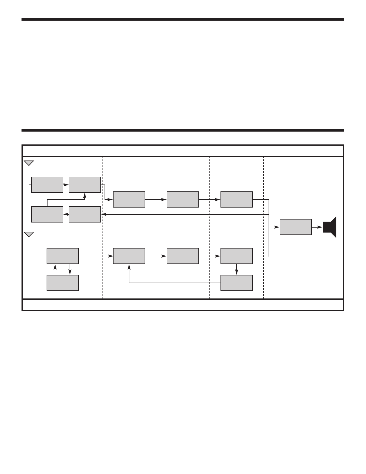
INTRODUCTION
The Elenco®Superhet 108T AM/FM Radio Kit is a
“superheterodyne” receiver of the standard AM (amplitude
modulation) and FM (frequency modulation) broadcast
frequencies. The unique design of the Superhet 108
allows you to place the parts over their corresponding
symbol in the schematic drawing on the surface of the
printed circuit board during assembly. This technique
maximizes the learning process while keeping the
chances of an assembly error at a minimum. It is very
important, however, that good soldering practices are
used to prevent bad connections. The Soldering Guide
should be reviewed before any soldering is attempted.
The actual assembly is broken down into 9 sections. The
theory of operation for each section, or stage, should be
GENERAL DISCUSSION
FM RADIO
Section 9
Section 8
Section 7 Section 6
read before the assembly is started. This will provide the
student with an understanding of what that stage has been
designed to accomplish, and how it actually works. After
each assembly, you will be instructed to make certain tests
and measurements to prove that each section is
functioning properly. If a test fails to produce the proper
results, a troubleshooting guide is provided to help you
correct the problem. If test equipment is available, further
measurements and calculations are demonstrated to
allow each student to verify that each stage meets the
engineering specifications. After all of the stages have
been built and tested, a final alignment procedure is
provided to peak the performance of the receiver and
maximize the Superhet 108T’s reception capabilities.
FM RF
AMPLIFIER
FM
OSCILLATOR
AM MIXER
OSCILLATOR
FM MIXER
1ST FM IF
AMPLIFIER
AFC
1ST AM IF
AMPLIFIER
AM
Section 3 Section 2
AM RADIO
The purpose of section 1, the Audio Amplifier Stage, is to
increase the po
detector to a power level capable of driving the speaker.
Section 2 includes the AM detector circuit and the AGC
(automatic gain control) circuit. The AM detector conv
the amplitude modulated IF (intermediate frequency)
signal to a low level audio signal. The AGC stage feeds
k a DC v
bac
maintain a near constant level of audio at the detector.
Section 3 is the second AM IF amplifier. The second AM
IF amplifier is tuned to 455kHz (Kilohertz) and has a fix
gain at this frequency of 50. Section 4 is the first AM IF 2
amplifier which has a variable gain that depends on the
oltage received from the AGC stage. The first AM
GC v
A
IF amplifier is also tuned to 455kHz. Section 5 includes
the AM mixer, AM oscillator and AM antenna stages.
When the r
induces a small voltage across the antenna coil. This
voltage is coupled to the mixer, or converter, stage to be
changed to a frequency of 455kHz.
accomplished by mixing (heterodyning) the radio
wer of the audio signal received from the
erts
oltage to the first AM IF amplifier in order to
ed
adio w
ave passes through the antenna, it
This change is
2ND FM IF
AMPLIFIER
2ND AM IF
AMPLIFIER
-3-
Figure 1
FM
DETECTOR
Speaker
AUDIO
AMPLIFIER
AM
DETECTOR
AFC
Section 1Section 5 Section 4
frequency signal with the oscillator signal. Section 6 is the
atio detector circuit. The FM ratio detector has a fixed
FM r
gain of about 20. Section 7 is the second FM IF amplifier.
The second FM IF amplifier is tuned to 10.7MHz
(Megahertz) and has a set gain of approximately 20. The
3dB bandwidth of this stage should be approximately
350kHz. Section 8 is the first FM IF amplifier. The first FM
IF amplifier is also tuned to 10.7MHz and has a set gain of
approximately 10. It also has a 3dB bandwidth of 350kHz.
Section 9 includes the FM mixer, FM oscillator, FM RF and
the AFC circuits.
The incoming r
by the FM RF amplifier, which is tuned to a desired radio
station in the FM frequency bandwidth of 88MHz to
108MHz.
These amplified signals are then coupled to the
FM mixer stage to be changed to a frequency of 10.7MHz.
This change, as in AM, is accomplished by heterodyning
adio frequency signal with the oscillator signal.
the r
AFC stage feeds back a DC voltage to the FM oscillator to
prevent the oscillator from drifting. Each of these blocks
will be e
xplained in detail in the
before the assembly instructions for that stage.
adio waves are amplified
The
Theory of Operation given
Page 5
CONSTRUCTION
Introduction
The most important factor in assembling your Superhet 108 AM/FM Transistor Radio Kit is good soldering
techniques. Using the proper soldering iron is of prime importance. A small pencil type soldering iron of 25 40 watts is recommended. The tip of the iron must be kept clean at all times and well tinned.
Safety Procedures
• Wear eye protection when soldering.
Locate soldering iron in an area where you do not have to go around it or reach over it.
•
• Do not hold solder in your mouth. Solder contains lead and is a toxic substance. Wash your hands
thoroughly after handling solder.
• Be sure that there is adequate ventilation present.
Assemble Components
In all of the following assembly steps, the components must be installed on the top side of the PC board unless
otherwise indicated. The top legend shows where each component goes. The leads pass through the
corresponding holes in the board and are soldered on the foil side.
Use only rosin core solder of 63/37 alloy.
Foil Side
DO NOT USE ACID CORE SOLDER!
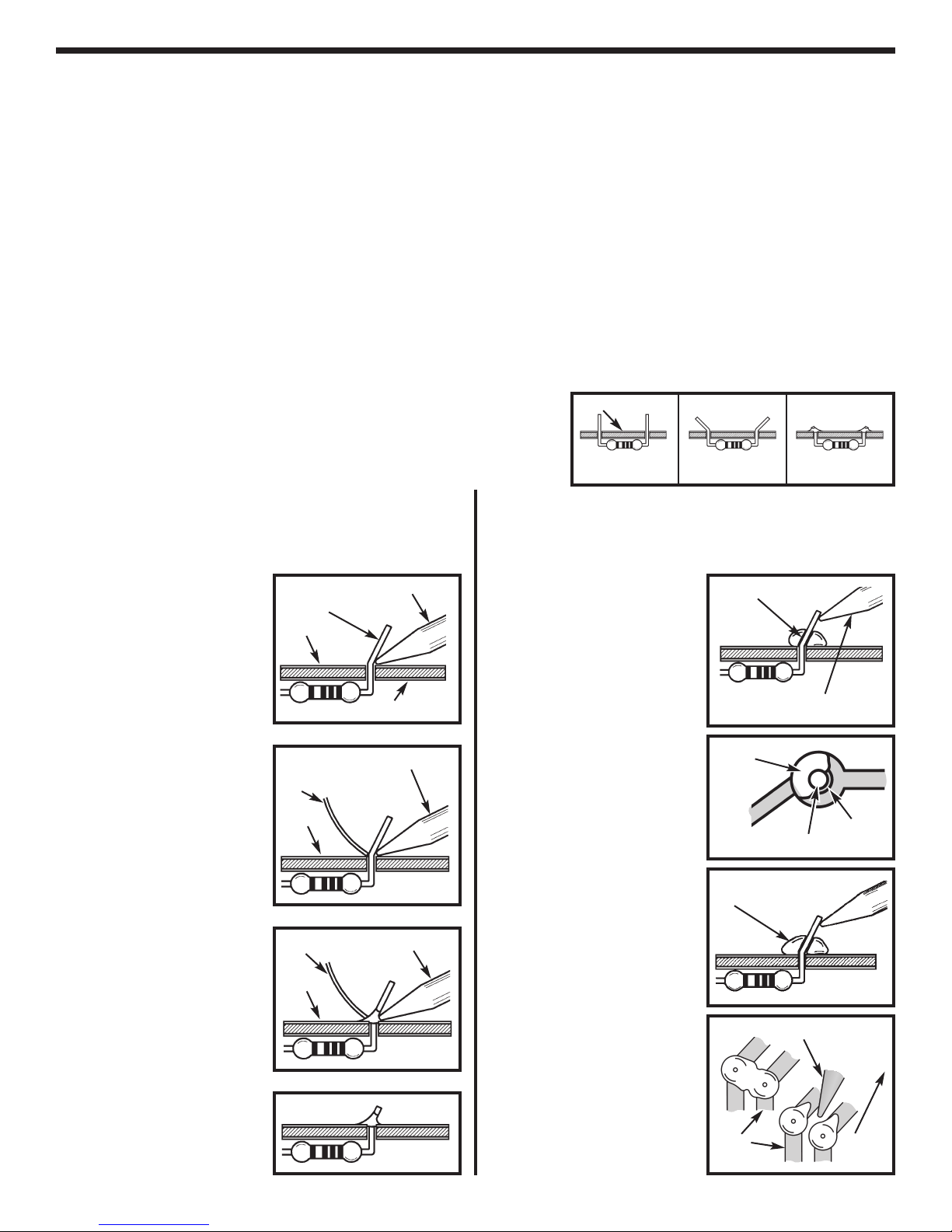
What Good Soldering Looks Like
A good solder connection should be bright, shiny,
smooth, and uniformly flowed over all surfaces.
1. Solder all components from
the copper foil side only.
Push the soldering iron tip
against both the lead and
the circuit board foil.
2. Apply a small amount of
solder to the iron tip. This
allows the heat to leave the
iron and onto the f
Immediately apply solder to
the opposite side of the
connection, away from the
iron. Allow the heated
component and the circuit
oil to melt the solder.
f
Allow the solder to flo
3.
around the connection.
Then, remove the solder
and the iron and let the
connection cool.
solder should have flowed
smoothly and not lump
around the wire lead.
4.
Here is what a good solder
connection looks like.
oil.
The
Component Lead
Foil
Solder
Foil
w
Solder
F
oil
Soldering Iron
Circuit Board
Soldering Iron
Soldering Iron
Mount Part
Bend Leads to
Hold Part
Solder and
Cut Off Leads
Types of Poor Soldering Connections
1. Insufficient heat - the
solder will not flow onto the
lead as shown.
2. Insufficient solder - let the
solder flow over the
connection until it is
vered. Use just enough
co
solder to co
connection.
3. Excessive solder - could
make connections that you
did not intend to between
adjacent foil areas or
minals.
ter
4. Solder bridges - occur
when solder runs between
circuit paths and creates a
short circuit. This is usually
caused by using too much
solder. To correct this,
simply dr
iron across the solder
bridge as shown.
ag y
ver the
our solder
ing
Rosin
Soldering iron positioned
incorrectly.
Solder
Component Lead
Solder
Solder
Foil
ing Iron
Dr
Gap
ag
-4-
Page 6
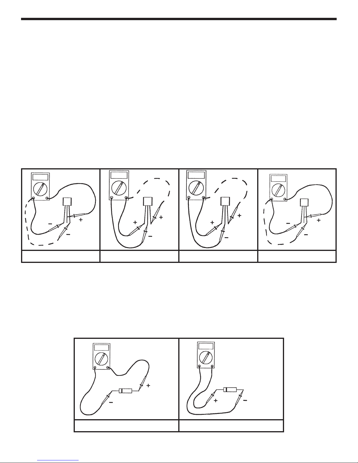
SEMICONDUCTOR PARTS FAMILIARIZATION
This section will familiarize you with the proper method used to test the transistors and the diode.
TRANSISTOR TEST
Refer to the parts list and find a NPN transistor. Refer
the Figure C (page 7) for locating the Emitter, Base and
Collector. Using an Ohmmeter, connect the transistor
as shown in Test A. Your meter should be reading a low
resistance. Switch the lead from the Emitter to the
Collector. Your meter should again be reading a low
resistance.
Refer to parts list and find a PNP transistor, refer to
Figure D (page 7) for locating the Emitter, Base and
Collector. Using an Ohmmeter, connect the transistor
as shown in Test C. Your meter should be reading a low
resistance. Switch the lead from the Emitter to the
Collector. Your meter should again be reading a low
resistance.
Using an Ohmmeter, connect the transistor as shown in
Test B. Your meter should be reading a high resistance.
Switch the lead from the Emitter to the Collector. Your
meter should again be reading a high resistance.
Typical results read approximately 1MΩ to infinity.
Low Resistance
Ω
OM
C
NPN
Ω
E
BC
COM
High Resistance
Ω
Ω
NPN
EBC
TEST A TEST B TEST C TEST D
Using an Ohmmeter, connect the transistor as shown in
Test D. Your meter should be reading a high resistance.
Switch the lead from the Emitter to the Collector. Your
meter should again be reading a high resistance.
Low Resistance
Ω
COM
Ω
PNP
E
BC
C
OM
High Resistance
Ω
PNP
Ω
E
BC
DIODE TEST
Refer to the parts list and find a diode. Refer to Figure E
(page 7) for locating the Cathode and Anode.
The end
with the band is the cathode. Using an Ohmmeter,
connect the diode as sho
wn in
Test E. Your meter
should be reading a low resistance. Using an
Low Resistance
Ω
COM
Ω
Diode
TEST E TEST F
Ohmmeter, connect the diode as shown in Test F. Your
meter should be reading a high resistance. Typical
results read approximately 1MΩ to infinity for silicon
diodes (1N4148).
High Resistance
Ω
COM
Ω
Diode
-5-
Page 7
SECTION 1
AUDIO AMPLIFIER
The purpose of the Audio Amplifier is to in-crease the
audio power to a level sufficient to drive an 8 ohm
speaker. To do this, DC (direct current) from the battery
is converted by the amplifier to an AC (alternating
current) in the speaker. The ratio of the power
delivered to the speaker and the power taken from the
battery is the efficiency of the amplifier. In a Class A
amplifier (transistor on over entire cycle) the maximum
theoretical efficiency is .5 or 50%, but in a Class B
amplifier (transistor on for 1/2 cycle) the maximum
theoretical efficiency is .785 or 78.5%. Since transistor
characteristics are not ideal, in a pure Class B
amplifier, the transistors will introduce crossover
distortion. This is due to the non-linear transfer curve
near zero current or cutoff. This type distortion is
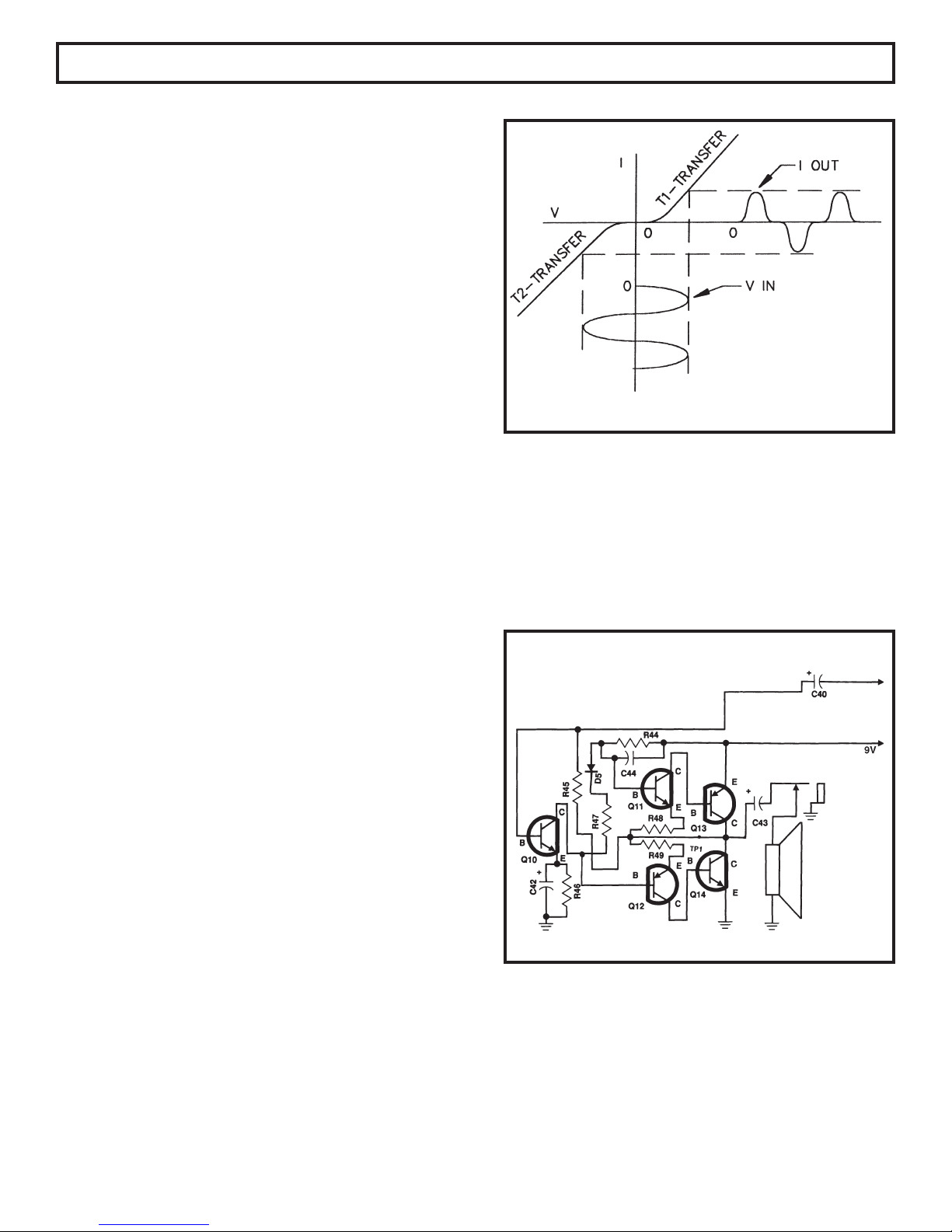
shown in Figure 2.
In order to eliminate crossover distortion and maximize
efficiency, the transistors (Q11 and Q12) of the audio
amplifier circuit are biased on for slightly more than 1/2
of the cycle, Class AB
are working as Class A amplifiers for very small levels
of power to the speaker, but they slide toward Class B
operation at larger power levels.
. In other words, the transistors
Figure 2
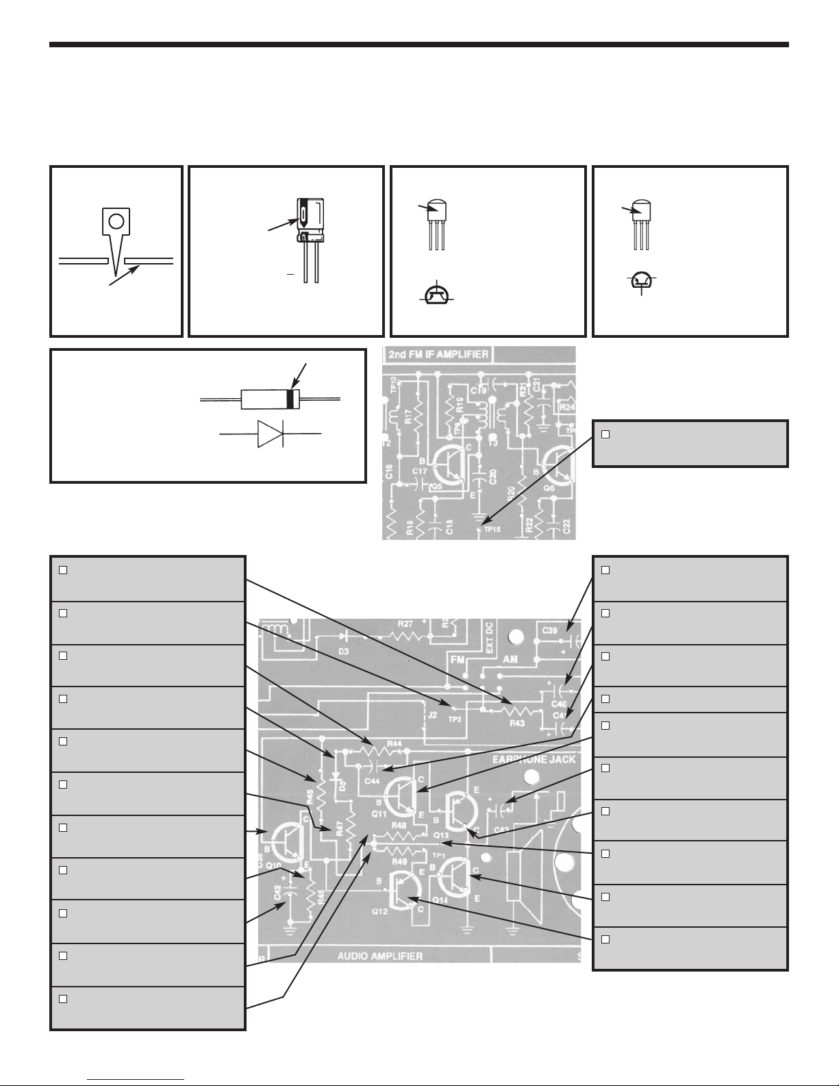
Transistor Q10 is a Class A amplifier that drives Q11
and Q12 through the bias string R44, D5 and R47. Q13
and Q14 are current amplifiers that amplify the current
of transistors Q11 and Q12. The AC and DC gain are
set by the DC current in transistor Q10 and the collector
resistor R44. The AC gain of the Audio Amplifier is
approximately equal to 100, while the DC gain equals
approximately 50. The transistors Q13 and Q14 self
bias so that the voltage at their emitters is
approximately 1/2 the supply voltage. R45 provides
feedback to the base of Q10 which is biased at
approximately .7 volts. Capacitor C40 couples the
audio signal from the v
audio amplifier. Capacitor C43 blocks the DC to the
speaker, while allowing the AC to pass.
olume control to the input of the
-6-
Page 8
ASSEMBLY INSTRUCTIONS
We will begin by installing resistor R43. Identify the resistor by its color and install as shown in Figure A. Be careful
to properly mount and solder all components. Diodes, transistors and electrolytic capacitors are polarized, be sure
to follow the instructions carefully so that they are not mounted backwards. Check the box when you have completed
each installation.
Test Point Pin
Foil Side
of PC Board
Figure A
Diode
Be sure that the
band is in the
correct direction.
R43 - 100Ω Resistor
(brown-black-brown-gold)
Lytic Capacitor
Polarity Mark
( )
(+)
Be sure that the negative lead is in
the correct hole on the PC board.
Figure B
Band
CathodeAnode
Figure E
NPN Transistor
Flat
Side
EBC
B
E
C
Figure C
Mount so E lead is
in the arrow hole
and flat side is in
the same direction
as shown on the
top legend. Leave
1/4” between the
part and PC board.
PNP Transistor
Flat
Side
EBC
E
B
Mount so E lead is
in the arrow hole
and flat side is in
the same direction
as shown on the
top legend. Leave
C
1/4” between the
part and PC board.
Figure D
TP15 - Test Point Pin
(see Figure A)
C39 - 470µF Lytic
(see Figure B)
TP2 - Test Point Pin
(see Figure A)
R44 -
3.3kΩ Resistor
(orange-orange-red-gold)
D5 - 1N4148 Diode
(see Figure E)
R45 - 470kΩ Resistor
(yellow-violet-yellow-gold)
R47 - 330Ω Resistor
(orange-orange-brown-gold)
Q10 - 2N3904 Transistor
(see Figure C)
R46 - 47Ω Resistor
(yellow-violet-black-gold)
C42 - 47µF L
ytic
(see Figure B)
R48 - 100Ω Resistor
wn-gold)
k-bro
lac
wn-b
(bro
R49 - 100Ω Resistor
(brown-black-brown-gold)
C40 - 10µF Lytic
(see Figure B)
C41 - 10µF Lytic
(see Figure B)
C44 - .001µF Discap (102)
Q11 - 2N3904 Transistor
(see Figure C)
C43 - 470µF Lytic
(see Figure B)
Q13 - MPS6562 or 8550
Transistor (see Figure D)
est Point Pin
T
TP1 -
(see Figure A)
Q14 - MPS6560 or 8050
ansistor (see Figure C)
r
T
Q12 - 2N3906 Transistor
(see Figure D)
-7-
Page 9
ASSEMBLY INSTRUCTIONS
Note: Mount the Pot/SW, earphone jack,
and speaker to the foil side of the PC
board.
Knob
Nut
Washer
Cut off
locating pin
Plastic Washer
Solder all 5 tabs to PC board
Figure F
Battery Holder
3 Screws 2-56 x 1/4”
3 Nuts 2-56
Solder and cut off
excess leads.
Volume/S2
(50kΩ Pot / SW)
with Nut & Washer
Plastic Washer
Knob (pot)
(see Figure F)
Earphone Jack
with Nut
(see Figure H)
Speaker
Speaker Pad
Wire #22 Insulated
(see Figures G & I)
Figure G
If the speaker pad has center and outside pieces, then
remove them. Peel the backing off of the speaker pad and
stick the pad onto the speaker. Then stick the speaker
onto the solder side of the PC board as shown.
Remove
Backing
Speaker
Figure H
Your kit may contain a different type of earphone jack. Before installing
the jack, determine which one you have.
Foil Side
2
3
GND Pad
Nut
1
Foil Side
2
3
1
GND Pad
Nut
Pad
1.5” Wire
Backing
1.5”
Figure I
Wire
1.5” Wire
er
T
From
minal 3
1 - GND
Tip
2 3 - N.C. Tip
Mount the jack with the nut from the foil side of the PC board (terminal #1
on the GND pad of the PC board). Be sure to line up the tab with the pad
on the copper side of the PC board.
PC board.
Part # 622130
1 - GND
Tip
2 3 - N.C. Tip
Solder terminal #1 to the pad of the
Part # 622131
1” Wire
ar
P
t # 622130
1” Wire
Part # 622131
1.5” Wire
Cut three wires 1”, 1.5” and 1.5” and strip 1/4” of insulation
off of both ends. Solder the 3 wires as shown. Save the
extra wire for the FM Section.
-8-
Page 10
STATIC MEASUREMENTS
POWER TEST
For all measurements, connect your equipment GND to
circuit GND TP15. Set your VOM (Volt-Ohm-Millimeter)
to read 2 amps DC. Connect the meter to the circuit as
shown in Figure 3. Make sure that the volume control
is in the OFF position (turned fully counter-clockwise).
While watching you VOM, turn the volume to the ON
position (rotate clockwise until a “click” is heard). The
VOM should indicate a very low current. Adjust your
meter for a more accurate reading if necessary. If the
current is greater than 20 milliamps, immediately turn
the power OFF. The current should be less than 10
milliamps. This is the current drawn by the battery
when no input signal is present (the “idle current”). Turn
OFF the power. If your circuit fails this test, check that
all of the parts have been installed correctly, and check
for shorts or poor solder connections.
+
--
+
--
A
Amps
COM
OUTPUT BIAS TEST
Put the battery into the holder.
Figure 3
TP15
COM
V
V
Figure 4
-9-
Page 11
Adjust your VOM to read 9 volts and connect it as
shown in Figure 4. Make sure that the battery, or a 9
volt power supply (if available), is properly connected
and turn the power ON. The voltage at TP1 should be
between 3 to 6 volts. If you get this reading, go on to
the next test. If your circuit fails this test, turn the power
TRANSISTOR BIAS TEST
Move the positive lead of your VOM to the base of Q11.
Make sure that the power is ON. The voltage should be
between .5 and .8V higher than the voltage at TP1. All
silicon transistors biased for conduction will have
approximately .7V from the base to the emitter. Now
move the positive lead of your VOM to the base of Q12.
The voltage at this point should be between .5 and .8V
If you do not have a variable power supply, skip to the next test.
DYNAMIC MEASUREMENTS
OFF and check that all of the transistors are correctly
inserted in the correct locations. The E on the transistor
indicates the emitter lead and should always be in the
hole with the E next to it. Check that all resistor values
are the correct value and not interchanged.
lower than the voltage at TP1. This is because Q12 is
a PNP type transistor. Turn the power OFF. If your
circuit fails this test, check the Q11 and Q12 are
properly inserted in the circuit board. All static tests
must pass before proceeding to the Dynamic Tests or
the next section.
DC GAIN
The DC gain of the audio amplifier is set by the current
in transistor Q10. Looking at the circuit and assuming
the output bias is 1/2 of V+ or 4.5 volts, the base of Q11
will be .7V higher or 5.2 volts. This is because there is
a negligible voltage drop across R48. This means there
is a 3.8 v
R44 can no
which equals 1.15 milliamps. Since D5 and R42 are
used for biasing transistors Q11 and Q12, the current
through Q10 can be assumed to be 1.15 milliamps.
The DC gain of Q10 can be calculated as the collector
oltage drop across R44. The current through
w be calculated as 3.8/R44 or 3.8/3.3k
resistor, R44, divided by the emitter resistor plus the
Effective Emitter Resistance. The effective emitter
resistance is actually the dynamic resistance of silicon
and can be calculated by the approximate equation:
Rj = 26 / I(in milliamps)
ore, Rj = 26 / 1.15 = 22.6 ohms. Now the DC gain
theref
can be calculated as:
R44 / (R46 + Rj) or 3300 / (47 + 22.6) which equals
47.4.
V
Figure 5
-10-
COM
TP15
V
Page 12
It is advisable to use a digital meter because of the
small voltage changes in the following test. Connect
your VOM to the circuit as shown in Figure 5. Set your
VOM to read 1 volt DC and turn the power ON. Record
the base of Q10 here:
Vb1 = _____ volts.
Now set your VOM to read 9 volts and connect the
positive lead to test point TP1. Record the output bias
voltage here:
Vo = ____ volts.
Turn the power OFF. With a 1M ohm resistor (brownblack-green-gold), R34, connect the power supply to the
circuit as shown in Figure 6.
+
–
Power Supply
TP15
Turn the radio ON and turn the power supply ON.
Increase the supply voltage until the voltage at TP1 is
equal to Vo. Now increase the voltage of the supply
until the voltage at TP1 decreases by 1 volt. Move the
positive lead of your VOM to the base of Q10 and
record the voltage here:
Vb2 = ______.
It may be necessary to change scales of your VOM for
a more accurate reading. Turn the power OFF and
disconnect the power supply. Since the DC gain equals
the DC change at the output divided by the DC change
at the input, the DC gain of the audio can be calculated
as: 1 / (Vb2 - Vb1). Your answer should be near the
calculated DC gain of 47.4.
1MΩ
R34
Figure 6
If you do not have an audio generator, skip the following test and go directly to Section 2.
AC GAIN
The AC gain can be calculated in the same manner as
the DC gain e
capacitor C42 bypasses the emitter resistor R46
leaving only the effective emitter resistance, and there
is a resistance seen at the output of Q13 and Q14.
AC gain of Q10 can be calculated as R44 / Rj or 3300
/ 22.6 which equals 146.
positive, there will be a current flowing in Q11, which we
will call I(Q11).
the Beta (β) of transistor Q13 or β x I(Q11). The total
current at the output is equal to I(Q11) x (1 + β). The
resistance of R48 is also seen at the output. The
resistance is eff
Assuming β of the output transistors are equal to 100
than the resistance seen at the output is equal to 1
ohm, 100 / 100. This means that there is a voltage
divider between the output and the 8 ohm speaker. The
signal is now divided down so that the output is equal
to the A
which equals 130. This is also true when the input
C (gain of Q10) x (8 / (1+8)), or 146 x (8 / 9)
xcept for two differences. For AC,
The
When the input signal is
This current will then be multiplied by
ely divided b
ectiv
y
β, R48 / β.
COM
TP15
signal is negative. The only difference is that Q12 and
Q14 are no
generator to the circuit as shown in Figure 7.
mally the AC gain is measured at a frequency of
Nor
1kHz. Your VOM, however may not be able to
accur
Therefore, it is recommended that this test be
ormed at 400Hz. Set the audio generator at 400Hz
perf
and minimum voltage output. With the power ON, set
your VOM to read an AC voltage of 1 volt at test point
TP1.
Slowly increase the amplitude of the audio generator
until y
generator at this setting and move the positive lead of
your VOM to the base of Q10. Record the AC input
voltage to the amplifier here:
w conducting. Connect the VOM and audio
oltages at this frequency
ately read A
Increase the v
OM reads 1 v
our V
C v
olume control about half w
C
olt A
Vin = __________ v
. Leave the audio
.
olts
-11-
V
V
.
ay.
Page 13
You may have to change scales on your VOM for the
most accurate reading. Turn the power OFF. The AC
voltage gain of your audio amplifier is equal to the AC
enerator
G
output voltage divided by the AC input voltage, or 1/Vin.
The gain should approximately equal the calculated
gain.
Hz
If an oscilloscope is not available, skip the following test and go directly to Section 2.
AC BANDWIDTH
Generator
Hz
TP15
Figure 7
COM
TP15
Oscilloscope
V
V
TP15
Connect the oscilloscope and audio generator to your
circuit as sho
wn in Figure 8.
Set the audio generator for a frequency of 1kHz and
minim
oltage output.
um v
Set the oscilloscope to read
.5 volts per division. Turn on the power and slowly
increase the v
olume control to a comfortable level.
Increase the amplitude of the audio generator until the
oscilloscope displays 2 volts peak to peak, (Vpp), at
It may be necessary to adjust the volume control.
TP1.
Move the oscilloscope probe to the base of Q10 and
record the input v
oltage here:
Vin = _______ Vpp
Figure 8
-12-
TP15
(at this point, you may want to verify the AC gain).
Move the oscilloscope probe back to TP1 and slowly
increase the frequency from the audio gener
ator until
the waveform on the oscilloscope drops to .7 of its
iginal reading (1.4Vpp or 2.8 divisions). The
or
frequency of the generator, when the output drops to
.7 of its original value, is called the high frequency 3
decibel (dB) cor
ner. Record this frequency here:
(f high 3dB) = __________ kHz.
Page 14
Slowly decrease the frequency of the generator until
the output drops to .7 of its original reading, 1.4Vpp or
2.8 divisions. This frequency is called the low
frequency 3dB corner - the low frequency 3dB corner or
(f high 3dB) - (f low 3dB). Your calculated answer
should be greater than 30kHz.
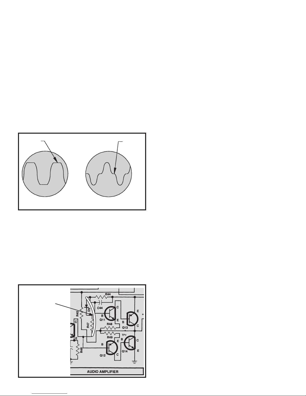
DISTORTION
Connect the generator and oscilloscope as shown in
Figure 8. Set the generator at a frequency of 1kHz, turn
the power ON and turn the volume to maximum. Adjust
the generator output until the peaks of the sinewave at
TP1 are clipped as shown in Figure 9A. One side of the
sinewave may clip before the other depending on the
DC centering at TP1. If oscillations are seen, connect
a clip lead from the GND of your generator to the GND
of the circuit.
Clipped
Crossover
Distortion
MAXIMUM POWER OUTPUT
The maximum power output before distortion due to
“clipping” can be calculated using the voltage Vclp
obtained in step 4 as follows:
Vpeak (Vp) = Vclp/2
Vroot mean squared (Vrms) = Vp x .7
Max power out = (Vrms)
Maximum power output should be greater than 350
milliwatts.
2
/8 ohms = (Vclp x .35)2/8
EFFICIENCY
By measuring the DC power taken from the battery at
the maximum power output level, the efficiency to the
audio amplifier can be calculated. Power from the
battery is equal to the current taken from the battery
times the voltage of the battery during maximum power
output. Efficiency can then be calculated as follows: Eff
= Max audio power/Battery power. It is best to use a
power supply (if available) to prevent supply voltage
from changing during these measurements. Connect
the generator, oscilloscope and current meter as shown
in Figure 11. Set your current meter to read 1 amp DC.
Turn the power ON and rotate the volume control to
maximum. Slowly increase the amplitude of the audio
ator until the output is clipped as shown in Figure
gener
Record Vclp here:
9A.
A
Measure the maximum voltage peak to peak when
clipping first occurs and record that value here:
Using a wire short out diode D5 and resistor R47 as
shown in Figure 10. The waveform should resemble
Figure 9B. The “flat spots” near the center of each
sinewave demonstrate what is called crossover
distortion. Most of this distortion should disappear when
you remove the shorting lead. Turn the power OFF.
Figure 9
Vclp = _______ Vpp.
B
Wire Lead
or Clip Lead
Vclp = _________ Vpp.
This should be equal to Vclp in step 4. Record the DC
current dr
Measure the supply voltage and record the V supply
here:
Turn the power OFF. Calculate the maximum power
output as done in the
awn from the 9 volt supply here:
Current (I) max = ________ Amps.
V supply = ________ volts.
Maximum Power Output Step.
Record your answers on the next page.
Figure 10
-13-
Page 15

Generator
Hz
TP15
TP15
If you do not have a power supply, use a 9
volt battery instead.
ower Supply
P
mps
A
mps COM
A
Figure 11
TP15
Vp = Vclp/2 Vp = ______
ms = Vp x .7 Vrms = ______
Vr
Max power out = (Vrms)
2
/8 Max power out = ______
Since the battery power equals the battery voltage times the current taken from the battery; calculate the battery
:
er
w
po
Battery power = Imax x V supply Battery power = ______
Since the efficiency (N) is equal to the Max power out divided by the Battery power, we can now calculate the
efficiency of the audio amplifier
er out/Batter
N = Max po
w
N in % = N x 100
.
er N = _______
w
y po
N = _______%
Your calculated answer should be around .6 or 60%.
-14-
Page 16
SECTION 2
AM DETECTOR AND AGC STAGE
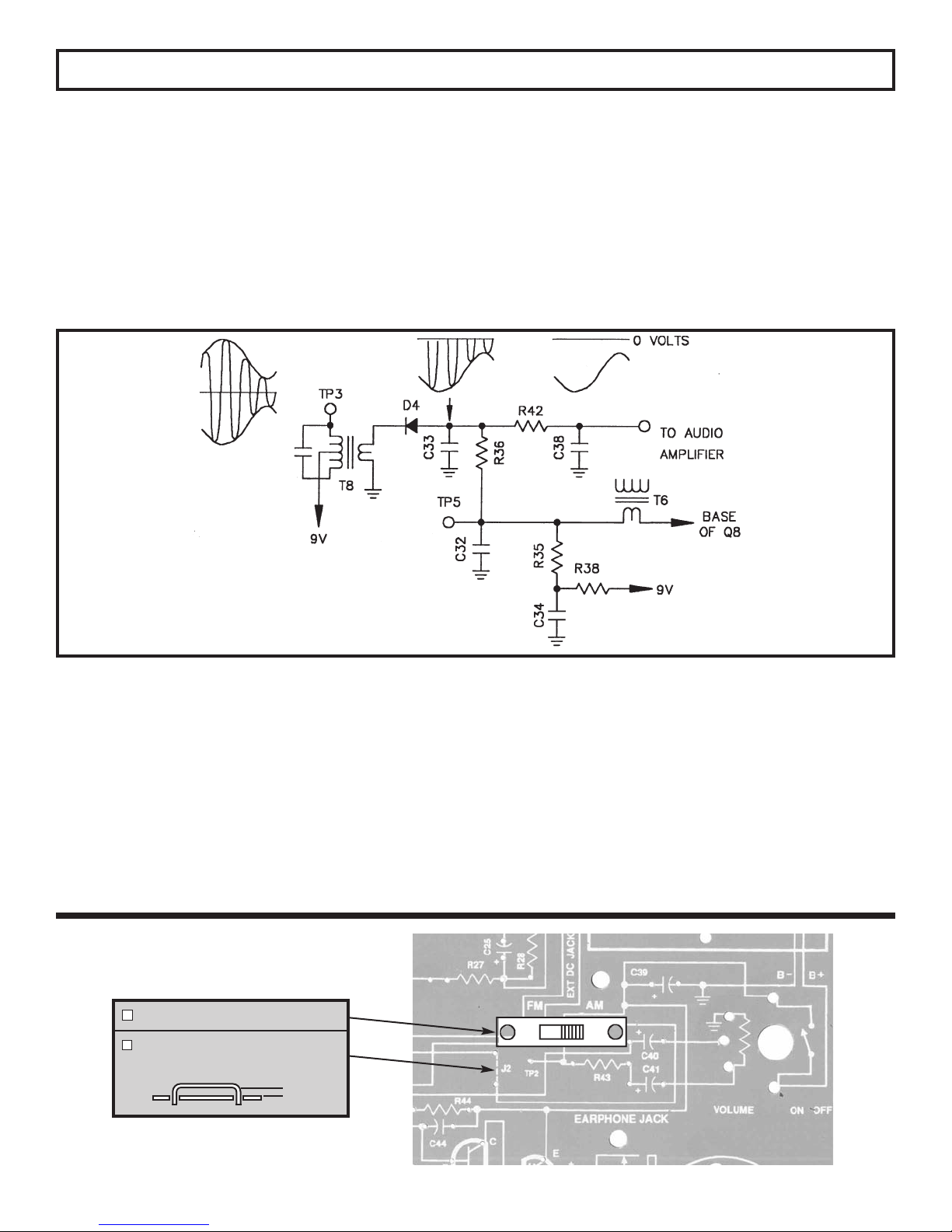
The purpose of the detector is to change the amplitude
modulated IF signal back to an audio signal. This is
accomplished by a process called detection or
demodulation. First, the amplitude modulated IF signal
is applied to a diode in such a way as to leave only the
negative portion of that signal (see Figure 12). The
diode acts like an electronic check valve that only lets
current pass in the same direction as the arrow (in the
diode symbol) points. When the diode is in conduction
(On Condition), it will force the capacitors C33 and C38
to charge to approximately the same voltage as the
negative peak of the IF signal. After conduction stops
in the diode (Off Condition), the capacitors will
discharge through resistors R36 and R42. The
discharge time constant must be small enough to follow
the audio signal or high frequency audio distortion will
occur. The discharge time constant must be large
enough, however, to remove the intermediate
frequency (455kHz) and leave only the audio as shown
in Figure 12.
Figure 12
The purpose of the automatic gain control (AGC) circuit
is to maintain a constant level at the detector,
regardless of the strength of the incoming signal.
Without AGC, the volume control would have to be
adjusted for each station and even moderately strong
stations would clip in the final IF amplifier causing audio
distortion. AGC is accomplished by adjusting the DC
bias of the first IF amplifier to lower its gain as the signal
strength increases. Figure 12 shows that the audio at
the top of the volume control is actually “riding” on a
negative DC voltage when strong signals are
ASSEMBLY INSTRUCTIONS
Switch
J2 - Jumper Wire
(use lytic lead)
1/8”
encountered. This negative DC component
corresponds to the strength of the incoming signal. The
larger the signal, the more negative the component. At
test point five (TP5), the audio is removed by a low pass
filter, R36 and C32, leaving only the DC component.
Resistor R35 is used to shift the voltage at TP5 high
enough to bias the base of transistor Q8 to the full gain
position when no signal is present. Resistors R35 and
R36 also forward bias diode D4 just enough to minimize
“On Condition” threshold voltage.
-15-
Page 17
ASSEMBLY INSTRUCTIONS
C34 - 100µF Lytic
(see Figure B)
T6 - AM IF Coil
(Yellow Dot)
27kΩ Resistor
R35 -
(red-violet-orange-gold)
TP5 - Test Point Pin
(see Figure A)
C32 - 10µF Lytic
(see Figure B)
R36 - 3.3kΩ Resistor
(orange-orange-red-gold)
C33 - .02µF (203)
or .022µF (223) Discap
R38 - 100Ω Resistor
(brown-black-brown-gold)
TP3 - Test Point Pin
(see Figure A)
T8 - AM IF Coil
(Black Dot)
D4 - 1N4148 Diode
(see Figure E)
C38 - .01µF Discap (103)
R42 - 2.2kΩ Resistor
(red-red-red-gold)
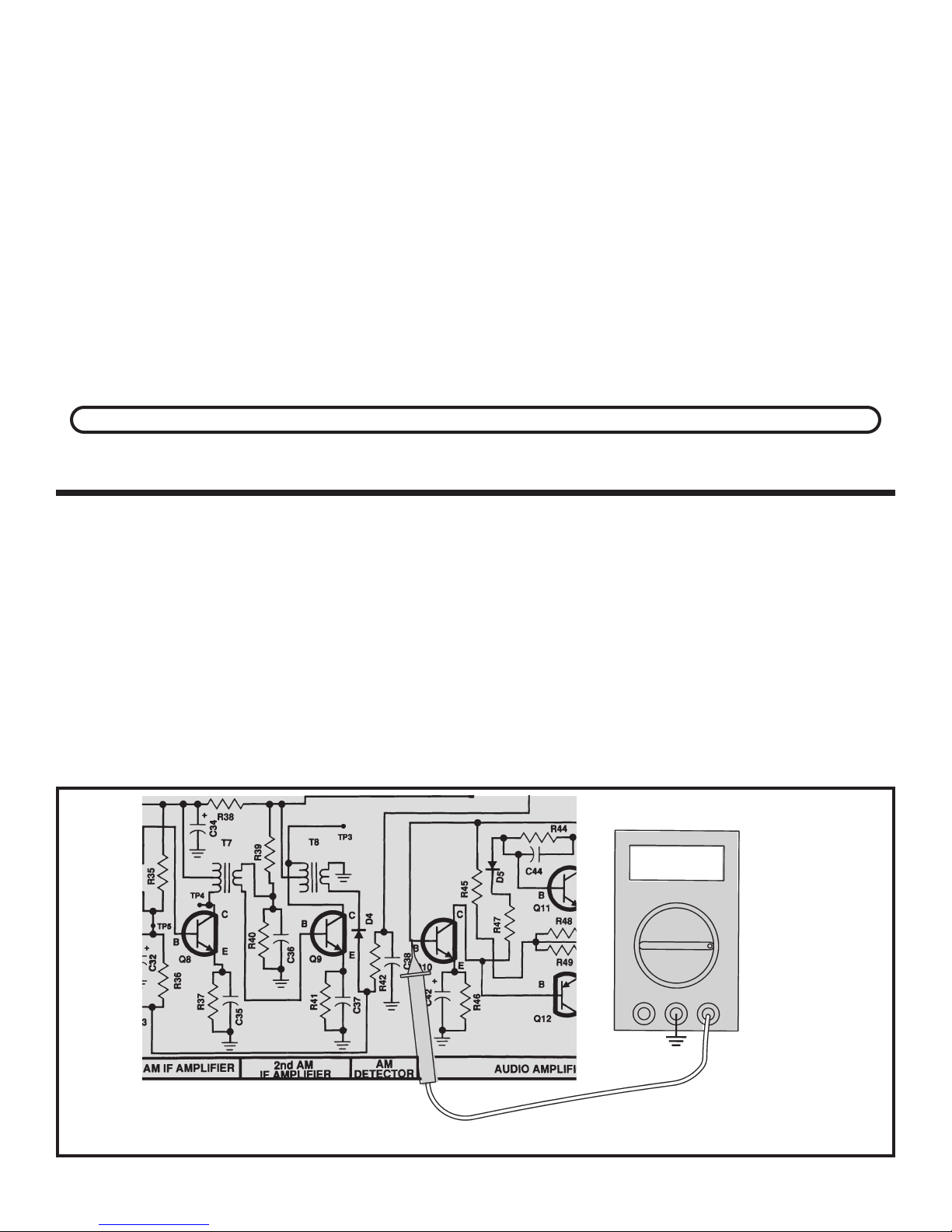
STATIC MEASUREMENTS
AGC ZERO SIGNAL BIAS
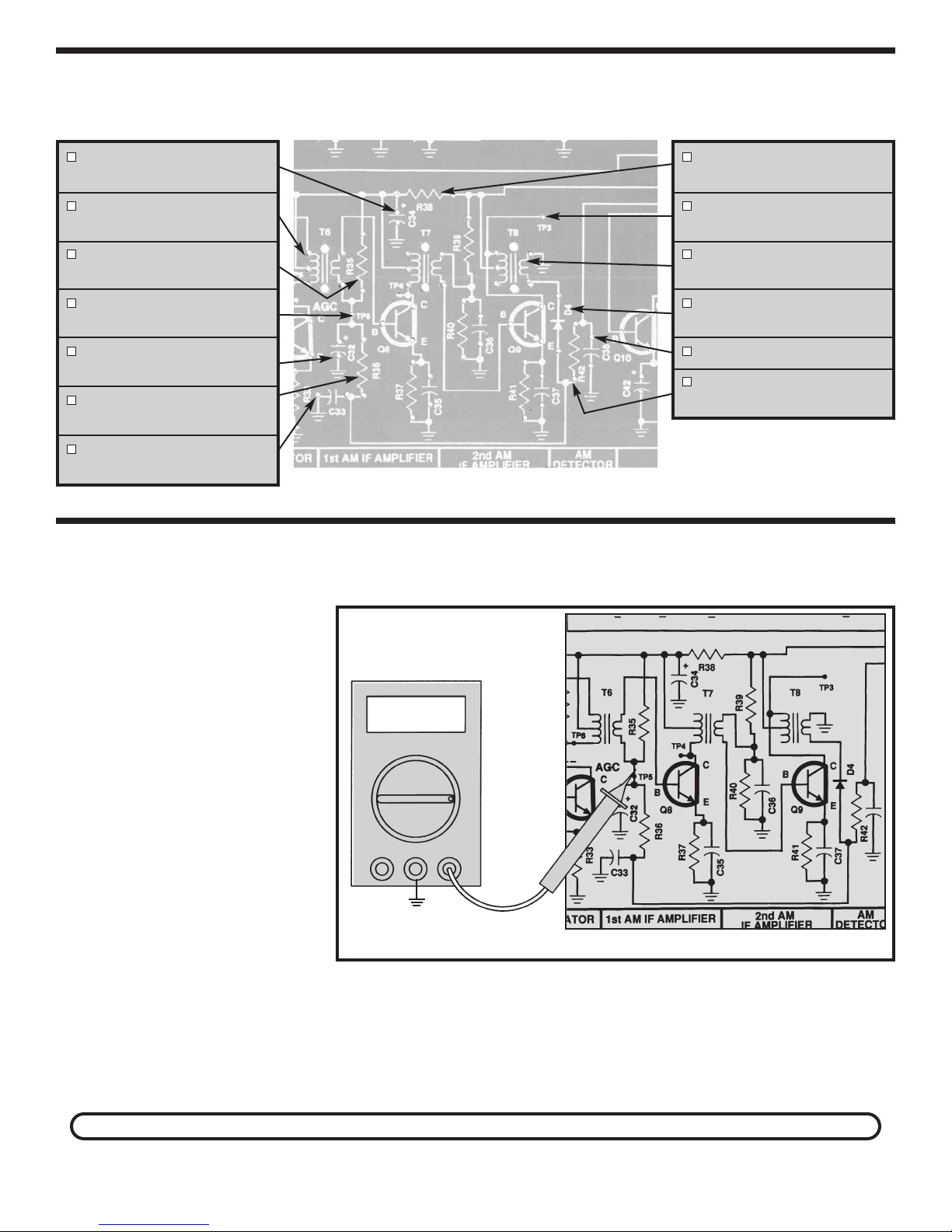
With the power turned OFF, connect your VOM to TP5 as shown in Figure 13. Make sure that the AM/FM switch is
in the AM position.
k that the VOM is adjusted to
Chec
read 9 volts DC and turn the power
ON. The voltmeter should read
approximately 1.5 volts DC. If your
reading varies by more than .5 volts
from this value, turn the power OFF
and check the polarity of D4. Also
check R36 and R35 and check that
ansformer T6 is properly installed.
tr
Amps COM V/Ω
TP15
T8 TEST
er turned OFF, connect the positive lead of
With the po
the VOM to TP3 and the negative lead to ground pin
TP15.
and turn the power ON. The voltage on the VOM should
w
e sure that the
Mak
OM is set to read 9 v
V
olts DC
V
Figure 13
be the same as y
voltage. If not, turn the power OFF and check that T8
is proper
ly installed.
our batter
T
y voltage or power supply
urn the po
wer OFF.
ou do not ha
If y
ve an RF g
-16-
enerator
, skip to Section 3.
Page 18
DYNAMIC MEASUREMENTS
AM DETECTOR AND AGC TEST
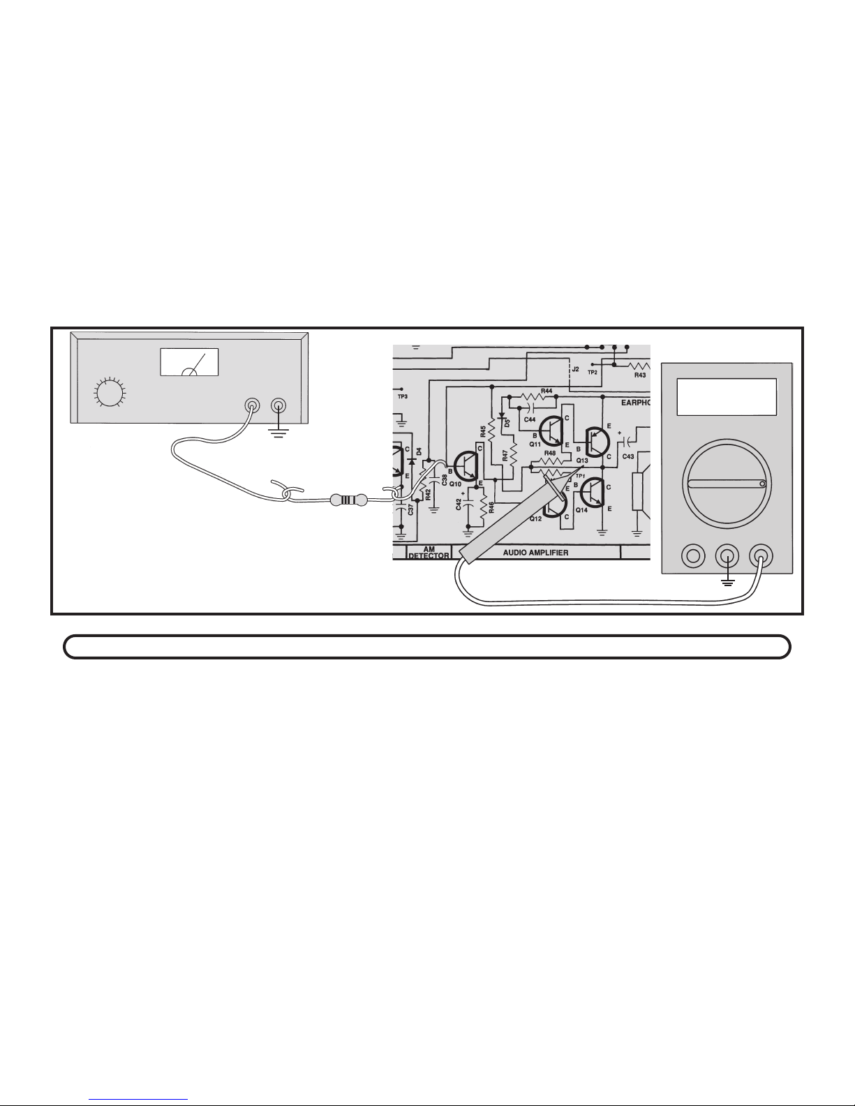
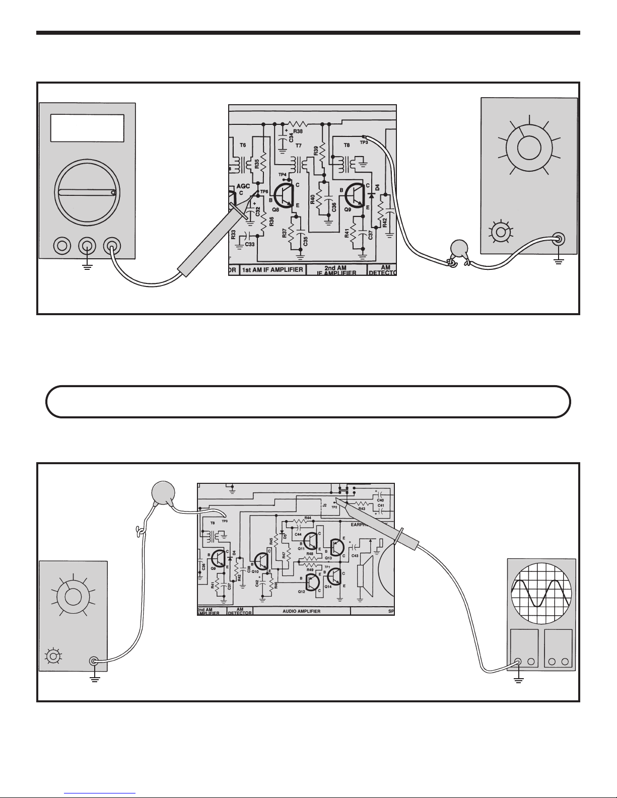
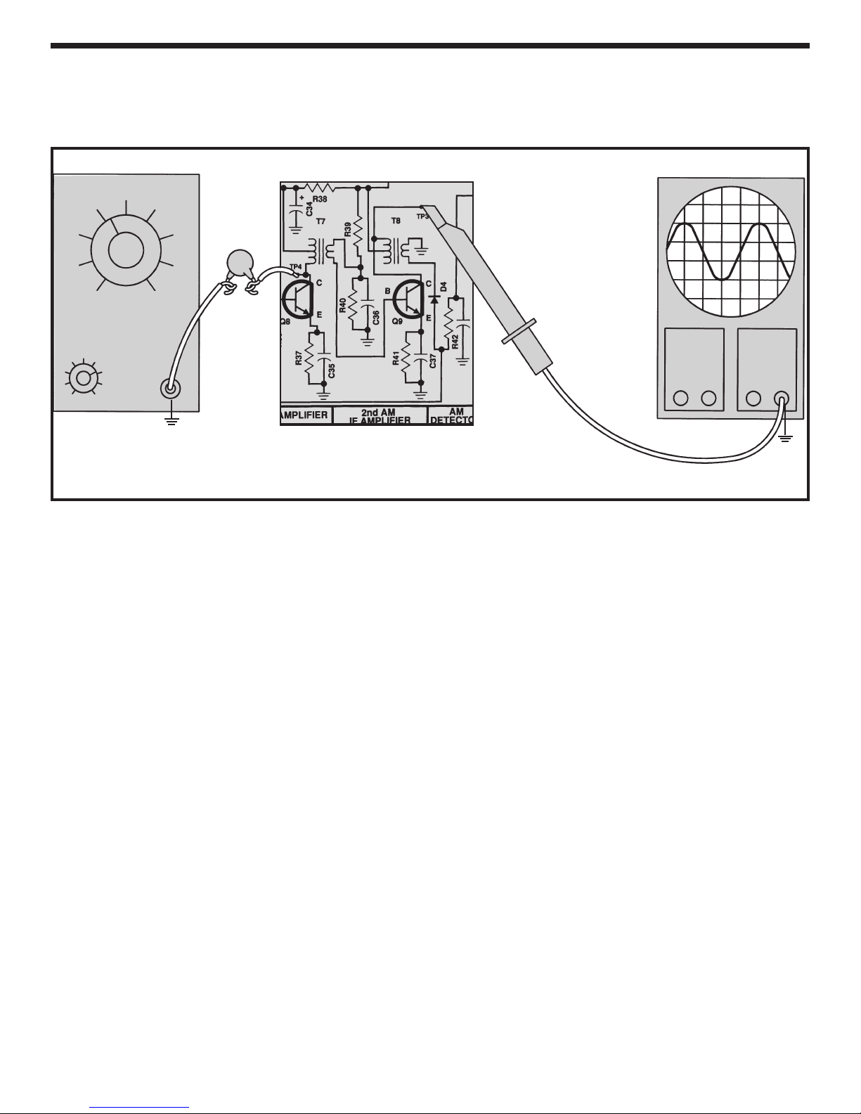
Connect your VOM and RF generator as shown in Figure 14.
V
Amps COM
V/Ω
Generator
Hz
.001µF
TP15
Figure 14
Set the VOM to accurately read 2 v
output of the RF generator for 455kHz, no modulation,
and minimum voltage output. Turn the power ON and
slowly increase the amplitude of the generator until the
If your RF generator does not have amplitude modulation and
olts DC and set the
you do not have an oscilloscope, skip to Section 3.
SYSTEM CHECK
Connect your equipment as shown in Figure 15.
.001µF
TP15
voltage at TP5 just starts to drop
. This point is called
the AGC threshold with no IF gain. Make a note of the
amplitude setting on the RF generator here:
____________.
Oscilloscope
Generator
Hz
TP15
Set the RF gener
ator at 455kHz, 1kHz at 80%
modulation and minimum voltage output. Turn the power
ON and set the v
olume control at maxim
adjust the amplitude of the RF generator output until you
um.
Figure 15
wly
Slo
TP15
hear the 1kHz tone on the speak
er. If this test fails, turn
the power OFF and check R42, D4 and TP5. Turn the
po
er OFF
w
.
-17-
Page 19

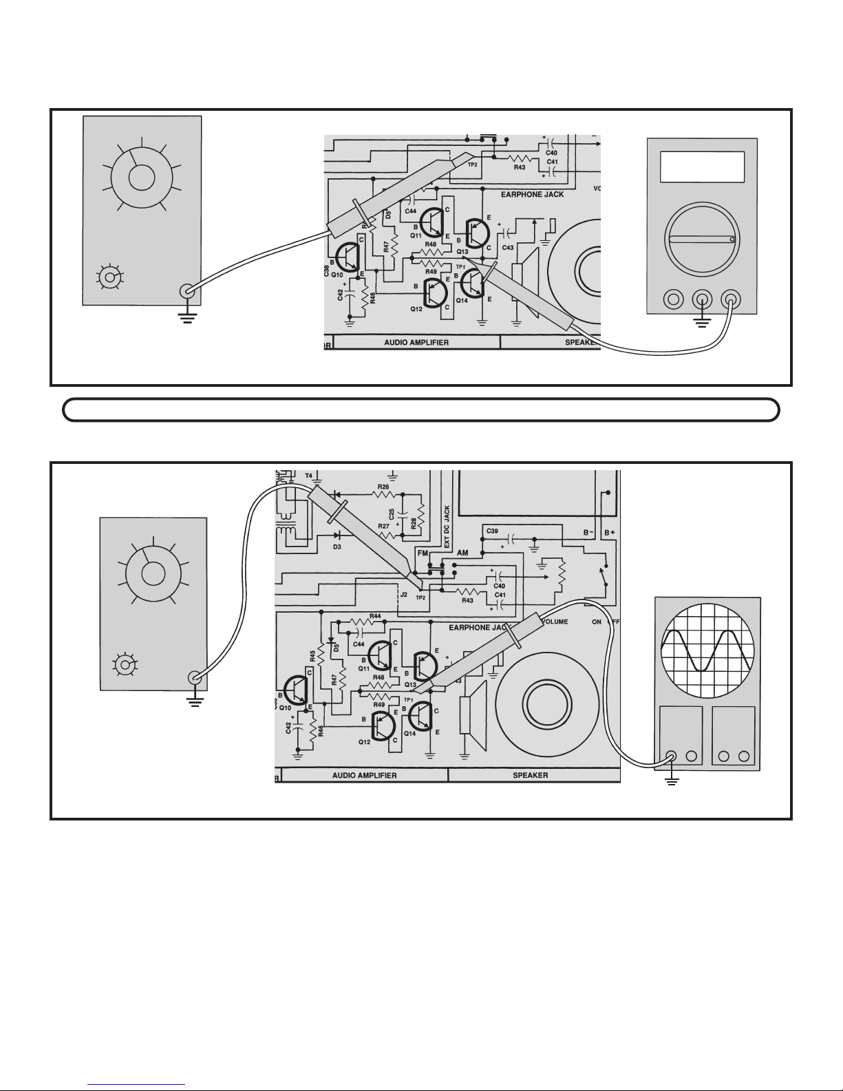
AM DETECTOR BANDWIDTH TEST
Connect your test equipment as shown in Figure 15.
Set the generator at 455kHz with 80% modulation at a
modulation frequency of 1kHz. Set the oscilloscope to
read .1 volts per division. Turn the power ON and set
the volume at the minimum. Increase the amplitude of
the generator until the signal on the oscilloscope is 4
divisions peak to peak. Check the signal to make sure
that it is free of distortion. Leave the frequency of the
SECTION 3
SECOND AM IF AMPLIFIER
The purpose of the second IF amplifier is to increase
the amplitude of the intermediate frequency (IF) and at
the same time provide SELECTIVITY. Selectivity is the
ability to “pick out” one radio station while rejecting all
others. The second IF transformer (T8) acts as a
bandpass filter with a 3dB bandwidth of approximately
6kHz. The amplitude versus frequency response of the
second IF amplifier is shown in Figure 16.
Both IF amplifiers are tuned to a frequency of 455kHz
and only need to be aligned once when the radio is
assembled. These amplifiers provide the majority of the
gain and selectivity needed to separate the radio
generator at 455kHz, but increase the modulation
frequency until the output drops to .28Vpp. Record the
modulation frequency on the generator here:
____________
This frequency should be greater than 5kHz. Turn the
power OFF.
stations.
The gain at 455kHz in the second IF amplifier is fixed
by the AC impedance of the primary side of transformer
T8, and the DC current in Q9. The current in Q9 is set
by resistors R39, R40 and R41. Both C36 and C37
bypass the 455kHz signal to ground, making Q9 a
common emitter amplifier. The signal is coupled from
the first IF amplifier to the second IF amplifier through
transformer T7. The IF transformers not only supply
coupling and selectivity, they also provide an
impedance match between the collector of one stage
and the base of the next stage. This match allows
maximum power to transfer from one stage to the next.
kHz
Figure 16
kHz
kHz
-18-
Page 20
ASSEMBLY INSTRUCTIONS
TP4 - Test Point Pin
(see Figure A)
T7 - AM IF Coil
(White Dot)
R40 - 10kΩ Resistor
(brown-black-orange-gold)
R41 - 470Ω Resistor
(yellow-violet-brown-gold)
STATIC MEASUREMENTS
Q9 BIAS
R39 - 39kΩ Resistor
(orange-white-orange-gold)
36 - .02µF Discap (203)
C
Q9 - 2N3904 transistor
(see Figure C)
C37 - .02µF (203)
or .022µF (223) Discap
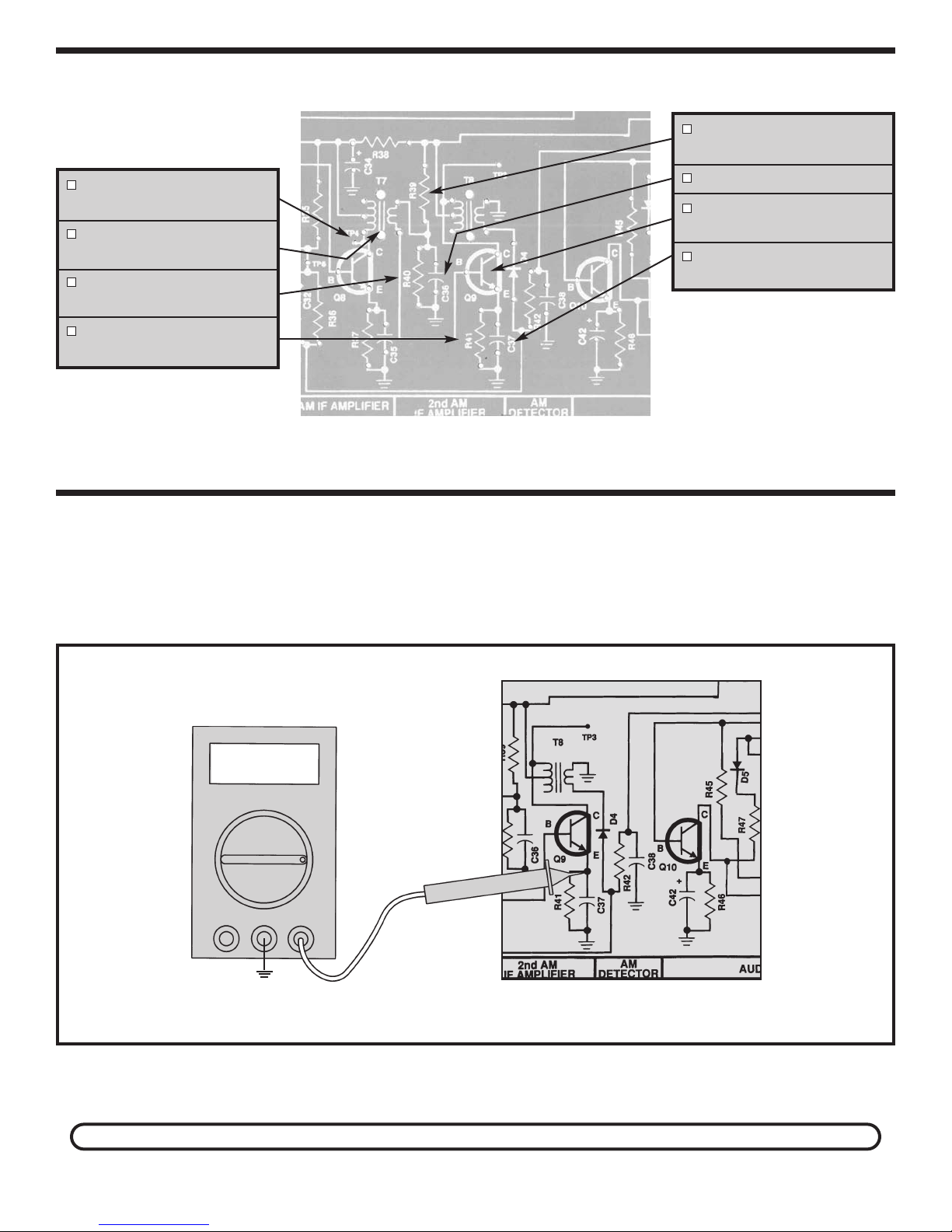
Connect your VOM as shown in Figure 17. Set the
VOM to read 9 volts DC and turn the power ON. The
voltage at the emitter of Q9 should be approximately 1
V
COM
Amps
V/Ω
TP15
volt. If your reading is different by more than .5 volts,
turn the power OFF and check components R39, R40,
R41 and Q9.
ou do not have an RF generator and oscilloscope, skip to Section 4.
If y
Figure 17
-19-
Page 21
DYNAMIC MEASUREMENTS
AC GAIN
Connect your test equipment as shown in Figure 18.
Generator
.02µF
Hz
TP15
Oscilloscope
Probe
TP15
Figure 18
Set the generator at 455kHz, no modulation and
minimum voltage output. Set the oscilloscope at 1 volt
per division.
capacitance of 50pF or less or it will detune
power ON and slowly increase the amplitude of the
generator until 4 volts peak to peak are seen on the
scope. With an alignment tool or screwdriver, tune T8
for a peak on the scope while re-adjusting the
generator’s amplitude to maintain 4 Vpp at the
oscilloscope. After T8 is aligned, move the scope probe
to the base of Q9 and record the peak to peak amplitude
of the signal here:
Turn the power OFF. The AC gain of the second IF
amplifier at 455kHz is equal to 4/Vb and should be
greater than 100. If your value is less than 50 check
components R39, R40, R41, C36 and C37. Also make
sure that Q9 is proper
The scope probe must have an input
T8. Turn the
Vb=________ Vpp.
ly installed.
n the po
ur
T
wer OFF.
BANDWIDTH
Reconnect your test equipment as shown in Figure 18.
Turn the power ON and adjust the generator for 4 volts
peak to peak at TP3. Realign T8, if necessary, for
maximum output while adjusting the output of the
generator to maintain 4Vpp at TP3. Slowly decrease
the frequency of the RF generator until the signal at
TP3 drops to .707 of its original value or 2.8Vpp.
Record the frequency of the RF generator here:
Fl = _______kHz.
Now increase the frequency of the generator past the
peak to a point where the signal drops to .707 of its
. Record that frequency here:
peak v
By subtracting the frequency of the lower 3dB corner
from the frequency of the higher 3dB corner you get the
bandwidth of the second IF amplifier
alue
Fh = __________kHz.
.
Calculate the bandwidth by (FI–Fh)
Bandwidth = __________kHz.
our results should be similar to the v
Y
Figure 16. Turn the power OFF.
-20-
alues sho
wn in
Page 22

SECTION 4
FIRST AM IF AMPLIFIER
The operation of the first IF amplifier is the same as the
second IF amplifier with one important difference. The
gain of the first IF amplifier decreases after the AGC
threshold is passed to keep the audio output constant at
the detector and prevent overload of the second IF
amplifier. This is accomplished by making the voltage
on the base of transistor Q8 lower as the signal strength
increases. Since the voltage from base to emitter is
fairly constant, the drop in voltage at the base produces
a similar drop in voltage at the emitter of Q8. This drop
ASSEMBLY INSTRUCTIONS
R34 - 1MΩ Resistor
(brown-black-green-gold)
TP6 - Test Point Pin
(see Figure A)
lowers the voltage across R37 and thus, reduces the DC
current through R37. Since all of the DC current from
the emitter of Q8 must go through R37, the DC current
in Q8 is therefore lowered. When the DC current in a
transistor is lowered, its effective emitter resistance
increases. The AC gain of transistor Q8 is equal to the
AC collector load of Q8 divided by its effective emitter
resistance. Raising the value of the effective emitter
resistance, thus, lowers the AC gain of Q8.
CAUTION: Test point must
not touch can of IF Coil.
STATIC MEASUREMENTS
Q8 BASE BIAS
VOM to the circuit as shown in Figure 13.
Connect y
Set your VOM to read 2 volts DC and turn the power
ON. The voltage at TP5 should be approximately 1.5
volts. If your circuit fails this test, check Q8 and R37.
Turn the power OFF.
our
Q8 - 2N3904 Transistor
(see Figure C)
C35 - .02µF (203)
or .022µF (223) Discap
R37 - 1kΩ Resistor
(brown-black-red-gold)
Q8 CURRENT
Connect the positiv
Q8 and connect the negative lead to ground point
TP15. Turn the power ON. The voltage should be
approximately .8 volts. Since the current in Q8 is equal
to the current in R37, I(Q2) = .8/R37 or approximately
.8 milliamps. Turn the power OFF.
e lead of y
our VOM to the emitter of
If you do not have an RF generator and oscilloscope, skip to Section 5.
-21-
Page 23

DYNAMIC MEASUREMENTS
.001µF
Hz
TP15
Short TP3 to R38 as shown below.
Oscilloscope
TP15
Figure 19
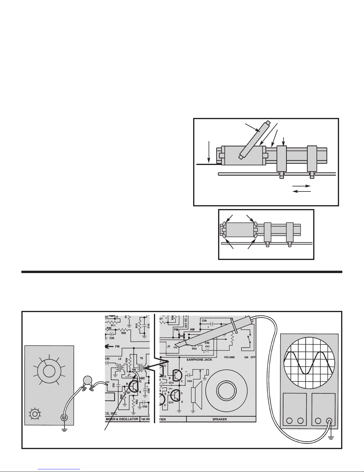
AC GAIN
Connect your test equipment as shown in Figure 19.
The scope probe must have an input capacitance of
12pF or less, otherwise it will detune transformer T7.
Using a clip lead, short TP3 to R38 as sho
short prevents the AGC from lower
first IF amplifier
modulation, and minimum voltage output. Set the
scope to read 1 volt per division and turn the power
ON. Increase the amplitude of the generator until
approximately 4Vpp is seen on the scope. Retune the
IF transformer T7 to maximize the 455kHz at TP4.
After tuning T7, adjust the generator amplitude in order
eep 4Vpp at TP4. Now move the scope probe to
to k
. Set the generator to 455kHz, no
ing the gain of the
wn. This
SECTION 5
AM MIXER, AM OSCILLATOR, AND AM ANTENNA
In a superheterodyne type receiver, the radio wave at
the antenna is amplified and then mixed with the local
oscillator to produce the intermediate frequency (IF).
Transistor Q7 not only amplifies the RF signal, but also
simulateously oscillates at a frequency 455kHz above
Positive feedback
the desired r
from the collector to the emitter of Q7 is provided by coil
L5 and capacitor C31.
adio station frequency
Dur
.
ing the heterodyning
the base of Q8 and record the peak to peak level of the
455kHz signal here:
Vb=___________Vpp
The AC gain of the first IF amplifier is equal to 4/Vb.
The AC gain should be greater than 100. DO NOT
TURN THE POWER OFF, GO TO THE NEXT TEST.
.
AGC ACTION
Move the scope probe back to TP4 and adjust the
generator for 4Vpp if necessary. Remove the clip lead
shorting TP3 to R38. The AGC should reduce the signal
level at TP4 to approximately .8 volts. Turn the power
.
OFF
process the following four frequencies are present at
the collector of Q7.
1. The local oscillator frequency, OF.
2. The RF carrier or radio station frequency.
The sum of these tw
3.
4. The difference of these two frequencies, LO - RF.
o frequencies
, LO + RF.
-22-
Page 24

The “difference frequency” is used as the intermediate
frequency in AM radios. The collector of Q7 also
contains an IF transformer (T6) tuned only to the
difference frequency. This transformer rejects all
frequencies except those near 455kHz. T6 also
couples the 455kHz signal to the base of Q8 to be
processed by the IF amplifiers. The antenna and the
oscillator coils are the only two resonant circuits that
change when the radio is tuned for different stations.
Since a radio station may exist 455kHz above the
oscillator frequency, it is important that the antenna
ASSEMBLY INSTRUCTIONS
C28 - .1µF Discap (104)
rejects this station and selects only the station 455kHz
below the oscillator frequency. The frequency of the
undesired station 455kHz above the oscillator is called
the image frequency. If the selectivity of the antenna (Q
factor) is high, the image will be reduced sufficiently.
The oscillator circuit must also change when the radio
is tuned in order to remain 455kHz above the tuning of
the desired radio station. The degree of accuracy in
keeping the oscillator frequency exactly 455kHz above
the tuning of the antenna is called tracking accuracy.
R31 - 56kΩ Resistor
(green-blue-orange-gold)
C30 - 150pF Discap (151)
L5 - AM Oscillator Coil
(Red Dot)
J1 - Jumper Wire
(use lytic lead)
L4 - AM Antenna w/ holders
(see Figures J & K)
C1 - Tuning Gang Capacitor
2 Screws #3
(see Figure L)
Knob (dial)
Screw #3
Label AM/FM
(See Figure M)
Note: Mount the tuning gang
capacitor to the f
the PC
board.
oil side of
Figure J
Resistance measurements
will be used to check the
configuration of the coil. Slide
one holder off the ferrite core
of the antenna assembly.
Then slide the coil off the the
errite core. Measure the
f
our
resistance of the coil.
readings should match the
appro
ximate v
alues as sho
Y
wn.
White
Black
Red
R=9 - 11Ω
}
}
R=1 - 1.5Ω
1/8”
TP7 - Test Point Pin
(see Figure A)
C31 - .01µF Discap (103)
Q7 - 2N3904 Transistor
(see Figure C)
R32 - 12kΩ Resistor
(brown-red-orange-gold)
R33 - 3.3kΩ Resistor
(orange-orange-red-gold)
C29 - .02µF Discap (203)
or .022µF Discap (223)
Wire3 Wire
4
White
R=9 - 11Ω
}
Black
Red
R=1 - 1.5Ω
}
Green
-23-
Page 25

IMPORTANT: Before installing the antenna coil, determine if you have a 3 wire coil or a 4 wire coil. Assemble it to the
PC board as shown below. Mount the antenna assembly to the PC board.
Put the tab of the first holder into the right hole and twist the tab 90O.
Put the tab of the second holder into the left hole and twist the tab 90O.
Slide the ferrite core through the holders.
Punch out one antenna shim from the front flap of the box.
Insert the cardboard antenna shim between the ferrite core and the
antenna coil. This will temporarily hold the coil in place.
Slide the antenna coil through the ferrite core.
Note: If the end of a wire from the antenna should break off, strip the
insulation off the end with a hot soldering iron. Lay the wire down on a hard
surface and stroke the wire with your iron. The insulation should come off
very easily. CAUTION: The soldering iron will burn the hard surface that you
are working on.
C (white)
B (black)
A (red)
C (white)
B
Twisted Together
Black
B Twisted Together
C (white)
Black
OR
Red
A (green)
Tabs
3 Wire Type Antenna: Solder the 3 colored wires to
the PC board: Wire A (red) to the hole marked
“RED”, Wire B (black) to the hole marked “BLK” and
Wire C (white) to the hole marked “WHT”.
Red
A (green)
4 Wire Type Antenna: Solder the 4 colored wires to the PC board: Wire A (green) to the
hole marked “RED”, Wire B (red and black twisted together) to the hole marked “BLK” and
Wire C (white) to the hole marked “WHT”.
Tabs
Figure K
It is important to know which of the two types of the tuning gang capacitor you have received with your kit. Look at the
gang capacitor that you have.
FM Antenna
Trimmer
FM Oscillator
Trimmer
FM SIDE
Locator Lead
AM SIDE
AM Antenna
Trimmer
AM Oscillator
Trimmer
AM Antenna
Trimmer
FM Antenna
Trimmer
FM SIDE
AM SIDE
AM Oscillator
Trimmer
FM Oscillator
Trimmer
Locator Lead
Mount the tuning gang capacitor to the foil side of the PC board with the
AM and FM sides in the correct direction. Fasten the gang in place with
two screws from the front of the PC board. Solder the leads in place and
cut off the excess leads coming through the PC board on the front side.
Figure L
-24-
Knob Post
w Holes
Scre
Page 26
ASSEMBLY INSTRUCTIONS
Figure M
Fasten the knob to the shaft of the
capacitor with a screw.
Rotate the knob fully clockwise.
Peel off the protective backing on
the label. Line up the long white
lines on the label with the arro
on the PC board.
Screw
Knob
ws
PC Board Stand
Insert the PC board into the stand as shown.
-25-
Page 27
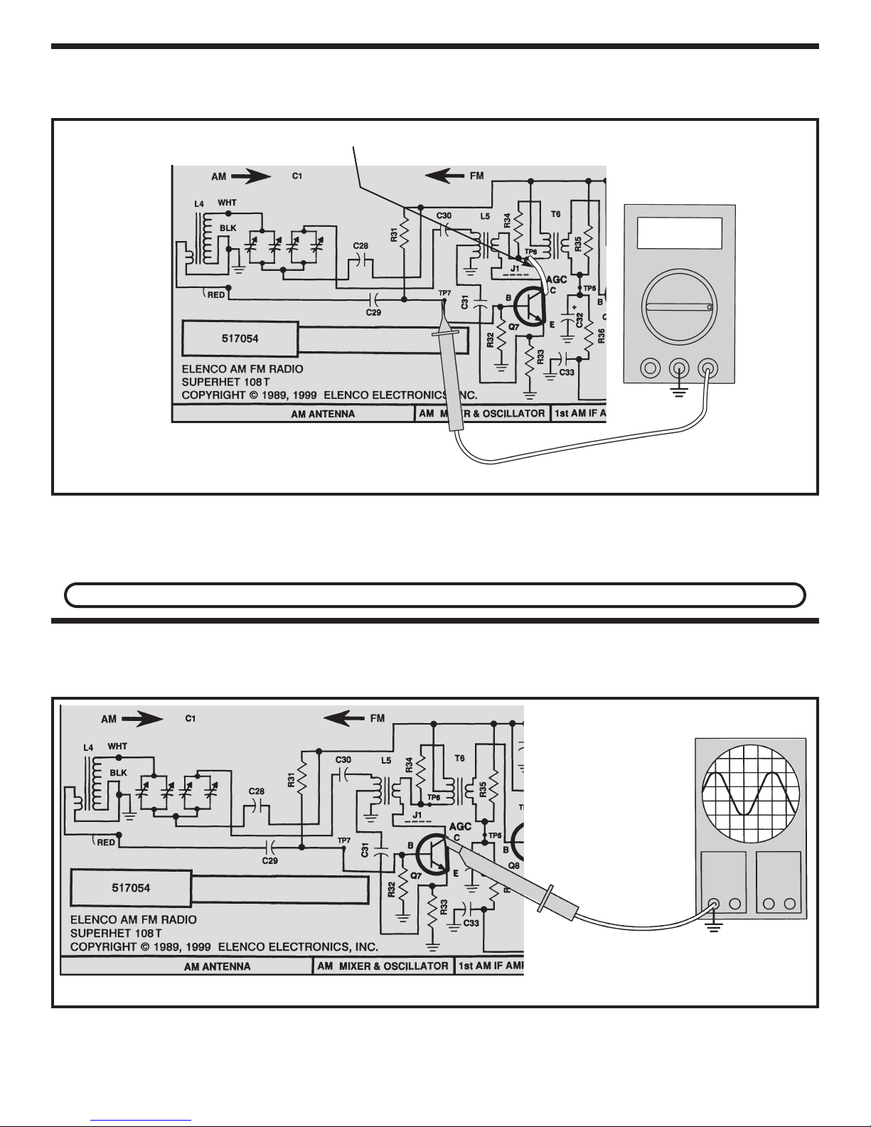
STATIC MEASUREMENTS
Q7 BIAS
Connect your VOM to the circuit as shown in Figure 20.
Short TP6 to the collector of Q7 as shown below.
V
COM V
TP15
Figure 20
Connect a clip lead from TP6 to the collector of Q7.
This short prevents Q7 from oscillating. Set the VOM to
read 2 volts DC and turn the power ON. The DC
voltage at TP7 should be about 1.6 v
If you do not have an oscilloscope, skip to the AM Final Alignments.
olts. If the voltage
in your circuit differs by more than .5 volts, leave the
power ON and check the battery voltage. If the battery
voltage is greater than 8.5 volts, check components
R31, R32, R33 and Q7. Tur
DYNAMIC MEASUREMENTS
AM OSCILLATOR CIRCUIT
Connect your test equipment to the circuit as shown in Figure 21.
n the power OFF.
Oscilloscope
Set the scope to read 1 volt per division and turn the
power ON. The scope should display a low voltage
sinewave. The frequency of the sinewave should
TP15
Figure 21
change when the tuning gang is turned. If your circuit
fails this test, check components Q7, gang capacitor,
C28, C29, C30, C31, L4 and L5. Turn the power OFF.
-26-
Page 28

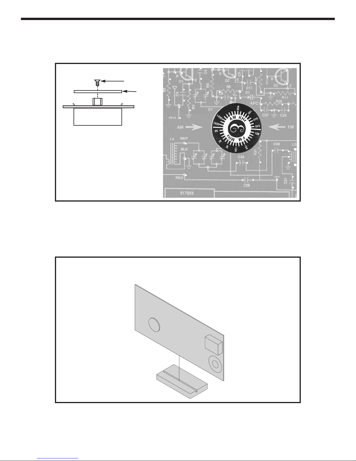
AM FINAL ALIGNMENTS
There are two different AM alignment procedures. The
first alignment procedure is for those who do not have
test equipment and the second is for those who do have
test equipment.
Included in your kit is a special device called a “magic
wand” which is used for aligning resonant circuits. It
usually has a piece of brass on one end and a piece of
iron on the other. When the brass end of the “magic
wand” is placed near the AM antenna, the antenna coil
will react as if inductance has been removed. Likewise,
when the iron end of the “magic wand” is placed near
the AM antenna, the antenna coil will react as if
inductance has been added. Therefore, when either
brass or iron is placed near the antenna coil, it will
change the inductance of the antenna coil. This change
in the inductance will cause the resonant frequency of
the circuit to change, thus changing the frequency at
which the antenna was selective. When aligning the
antenna and oscillator circuits, coils L4 and L5 are
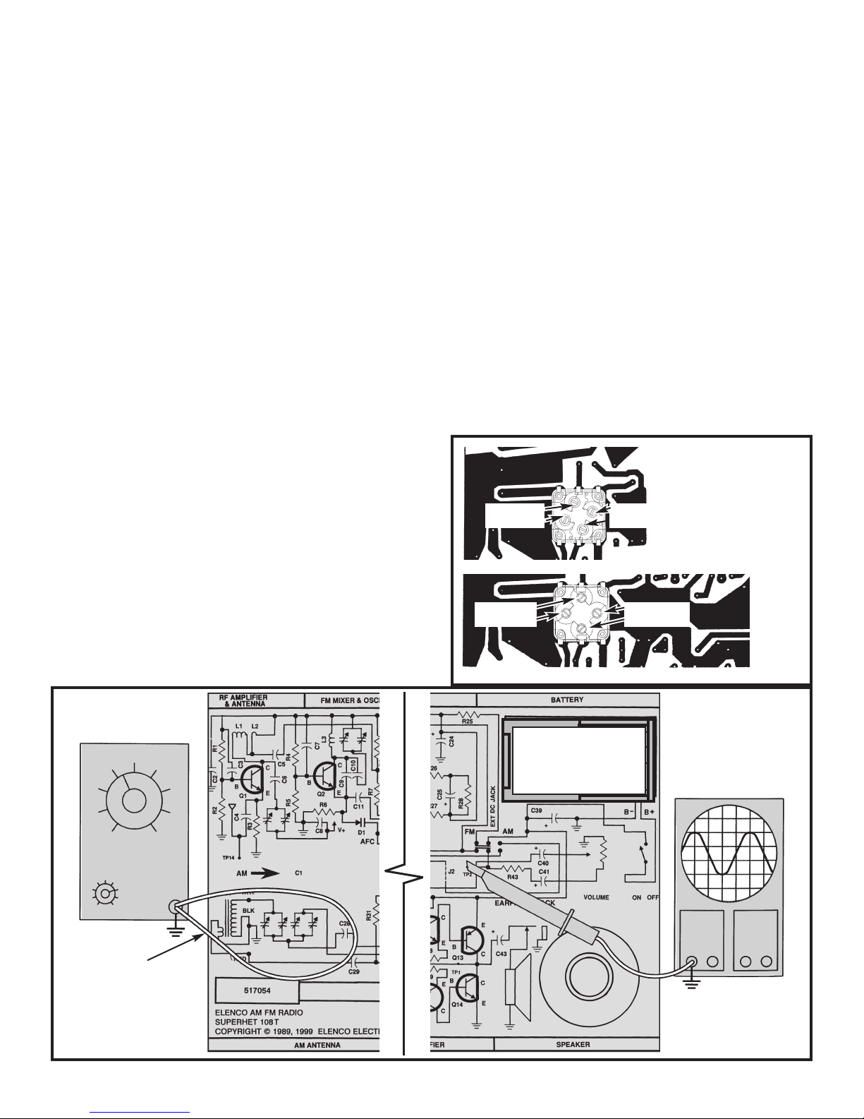
adjusted at the lower end of the band, while the
oscillator and antenna trimmer capacitors are adjusted
at the higher end of the band.
antenna and the oscillator will tr
This is done so that the
ack correctly.
AM ALIGNMENT WITHOUT TEST
EQUIPMENT
It is best to use an earphone for this procedure. Make
sure that the switch is in the AM position. With an
alignment tool or screwdriver, turn coils L5, T6, T7 and
T8 fully counter clockwise until they stop. DO NOT
FORCE THE COILS ANY FURTHER. Turn each coil in
about 1 1/4 to 1 1/2 turns. Set the AM antenna coil about
1/8” from the end of its ferrite rod. Refer to Figure K.
IF ALIGNMENT
Turn the power ON and adjust the volume to a
comfortable level. Turn the dial until a weak station is
heard. If no stations are present, slide the antenna back
and forth on its ferrite core, and retune the dial if
necessary. Adjust T6 until the station is at its loudest.
Reduce the volume if necessary. Adjust T7 until the
station is at its loudest and reduce the volume if
necessary. Adjust T8 until the station is at its loudest
and reduce the volume if necessary. Retune the radio
for another weak station and repeat this procedure until
there is no more improvement noticed on the weakest
possible station. This process peaks the IF amplifiers
to their maximum gain.
Soldering Iron Tip
Shrink Tubing
Iron Slug
Brass Slug
Magic Wand Assembly
Place the piece of brass inside the end of the
shrink tubing, with 1/4” outside. Heat the brass up
with y
our solder
around the br
other end in the same manner
ing iron until the tubing shrinks
ass. Assemble the iron piece to the
.
OSCILLATOR ALIGNMENT
Tune the r
is heard.
until their broadcast frequency is announced. If no
stations are present at the low side of the AM band,
adjust L5 until a station is heard. Once a station is
found and its broadcast frequency is known, rotate the
dial until the white pointer is aligned to that station’s
frequency marking on the dial. Adjust L5 until the
station is heard. Tune the radio until a known station
around 1400kHz is heard. It may be necessary to listen
to the station until their broadcast frequency is
announced. If no stations are present, adjust the AM
oscillator trimmer on the gang until a station is heard
(refer to Figure L). Once a station is found and its
broadcast frequency is known, rotate the dial until the
white pointer is aligned to that station’s frequency
marking on the dial. Adjust the AM oscillator trimmer on
the gang until the station is heard. Repeat these 2
steps until the oscillator alignment is optimized. This
process sets the oscillator range at 955kHz to
2055kHz.
adio until a known AM station around 600kHz
It may be necessary to listen to the station
-27-
Page 29
ANTENNA ALIGNMENT
Tune the radio for a station around 600kHz. With the
“magic wand” place the brass end near the antenna coil
as shown in Figure 23. If the signal heard at the output
increases, it means that the antenna coil needs less
inductance. To remove inductance, carefully slide the
antenna coil along it’s ferrite core in the direction shown
in Figure 23. Place the iron end of the “magic wand”
near the antenna coil. If the signal heard at the output
increases, this means that the antenna coil needs more
inductance. To add more inductance, carefully slide the
antenna coil along its ferrite core in the direction shown
in Figure 23. Repeat these steps until the signal heard
decreases for both ends of the “magic wand”. Tune the
radio for a station around 1400kHz. With the “magic
wand”, place the brass end near the antenna coil. If the
signal heard at the output increases, it means that the
antenna coil needs more capacitance. Adjust the
antenna trimmer on the back of the gang until the signal
is at its loudest. Refer to Figure 25 for the location of
the antenna trimmer. Place the iron end of the “magic
wand” near the antenna coil. If the signal heard at the
output increases, it means that the antenna coil needs
less capacitance
back of the gang until the signal is at its loudest.
Repeat these steps until the signal heard decreases for
both ends of the “magic wand”. Since the adjustment of
both the antenna trimmer and antenna coil will effect
the antenna alignment, it is advisable to repeat the
entire procedure until the antenna alignment is
optimized. This process sets the tr
radio section. Once the antenna is properly aligned,
. Adjust the antenna trimmer on the
acking of the AM
CAREFULLY APPLY CANDLE WAX or glue to the
antenna coil and the ferrite rod to prevent it from
moving (see Figure 23A).
This concludes the alignment of the AM radio section.
If no stations are heard, verify that AM signals are
present in your location by listening to another AM radio
placed near the Superhet 108T. If the AM section is still
not receiving, go back and check each stage for
incorrect values and for poor soldering. Proceed to the
FM assembly section.
ntenna Coil
Magic Wand
Antenna
Shim
If the antenna needs:
• More inductance, slide the coil
• Less inductance, slide the coil
A
Ferrite Core
Antenna Holder
Figure 22
Wax
Wax
Figure 23
AM ALIGNMENT WITH TEST EQUIPMENT
IF ALIGNMENT
Connect your RF generator and oscilloscope as shown
in Figure 24. Make sure that the switch is in the AM
Figure 24
Generator
.001µF
Hz
TP6 to the collector Q7.
t
TP15
Shor
position. Place a short from the collector of Q7 to TP6.
This short “kills” the AM oscillator.
Oscilloscope
TP15
-28-
Page 30
Set the RF generator at 455kHz, modulation of 400Hz
80% and minimum voltage out. Set the oscilloscope to
read .1 volts per division and turn the power ON.
Increase the amplitude of the generator until the
oscilloscope shows a 400Hz sinewave 5 divisions or .5
volts pp. With an alignment tool or screwdriver adjust
T6 for a peak. Reduce the generator amplitude so that
5 divisions are maintained. Adjust T7 for a peak and
reduce that amplitude again if necessary. Repeat these
steps to optimize the IF alignment. This process aligns
the IF amplifiers to 455kHz.
After the IF alignment is complete, lower the frequency
of the generator until the voltage drops .707 of its
peaked value or .35Vpp. Record the frequency of the
lower 3dB corner here:
Fl = _________kHz.
ON and set the volume control to a comfortable level.
Turn the tuning knob counter-clockwise until the white
pointer is aligned at the 540kHz marking on the dial.
With an alignment tool or screwdriver adjust L5 until a
400Hz tone is heard. Adjust L5 for a peak on the
oscilloscope. Adjust the amplitude of the RF generator
to maintain a level of .5 volts peak to peak or less. After
peaking L5, set the generator frequency to 1600kHz.
Turn the tuning knob clockwise until the white pointer is
aligned to the 1600kHz marking on the dial. With an
alignment tool or screwdriver, adjust the AM oscillator
trimmer on the back of the tuning gang until a 400Hz
tone is heard. Adjust the trimmer for a peak on the
oscilloscope. Refer to Figure 25 for the location of the
AM oscillator trimmer. Repeat these steps to optimize
the oscillator alignment. This process sets the oscillator
range at 955kHz to 2055kHz.
Increase the frequency of the generator past the peak
until the voltage seen on the scope drops .707 of its
peaked value or .35Vpp. Record the frequency of the
high 3dB corner here:
Fh = __________kHz.
The bandwidth of the IF is equal to BW = Fh - Fl. The
IF’s bandwidth should be around 6kHz. Turn the power
OFF and remove the short from the collector of Q7
to TP6.
Calculate the bandwidth: ___________kHz.
OSCILLATOR ALIGNMENT
Set the RF gener
modulation and a low level of output. Turn the power
Generator
ator at 540kHz, 400kHz 80% AM
ANTENNA ALIGNMENT
With the power turned OFF, connect your test
equipment as shown in Figure 26.
Figure 25
AM Antenna
FM Antenna
AM Oscillator
AM Antenna
Battery
AM Oscillator
FM Oscillator
FM Oscillator
FM Antenna
Oscilloscope
Hz
TP15
Wire loop
close to
antenna
Figure 26
TP15
-29-
Page 31

Set the generator at 600kHz, 400Hz 80% modulation,
moderate signal strength. Set the oscilloscope to read
.1 volts per division. Turn the tuning knob fully counterclockwise and turn the power ON. Slowly turn the tuning
knob clockwise until a 400Hz sinewave is seen on the
scope. Adjust the volume control to a comfortable level.
If a station exists at 600kHz, then lower the frequency of
the generator and repeat the previous steps. With the
“magic wand”, place the brass end near the antenna coil
as shown in Figure 23. If the signal on the scope
increases, it means that the antenna coil needs less
inductance. To add more inductance, carefully slide the
antenna coil along it’s ferrite core in the direction shown
in Figure 23. Repeat these steps until the signal seen
decreases for both ends of the “magic wand”. Increase
the frequency of the generator to 1400kHz and turn the
tuning knob clockwise until a 400Hz sinewave is seen
on the scope. If a station exists at 1400kHz, increase
the frequency of the generator and repeat the previous
AM RADIO HIGHLIGHTS
steps. Place the brass end of the “magic wand” near the
antenna coil. If the signal increases, it means that the
antenna coil needs less capacitance. Adjust the
antenna trimmer for a peak. Refer to Figure 25 for the
location of the AM antenna trimmer. Since the
adjustment of both the antenna alignment is optimized.
This process sets the AM tracking of the Superhet 108T.
Once the antenna is properly aligned, carefully apply
candle wax or glue the antenna coil to the ferrite rod to
prevent it from moving. Proceed to the FM assembly
section.
This concludes the alignment of the AM radio section.
If no stations are heard, verify that AM signals are
present in your location by listening to another AM radio
placed near the Superhet 108T. If the AM section is still
not receiving, go back and check each stage for
incorrect values and for poor soldering. Proceed to the
FM assembly section.
1. The number of vibrations (or cycles) per second
produced by a sound is called the frequency, and is
measured in hertz.
2. The distance between peaks of sound waves is
called the wavelength.
3. Sound waves are produced as a certain number of
vibrations per second. The more vibrations per
second, the higher the frequency; the fewer
ations, the lower the frequency.
vibr
Waves of v
4.
waves and travel great distances through the air
without the use of wires.
5. Carrier waves are radio waves used by broadcast
stations to carry audio waves.
ery high frequency are called radio
6. The process of adding the audio waves to the radio
7. The amount of signal picked up by the antenna will
8.
9. Heterodyning is the process of mixing two signals
DC VOLTAGES
The voltage readings below should be used in
troubleshooting the AM section. (Switch at AM
position).
TP1 3.9
Q7 B 1.5 Q11 B 4.4
E 1.1 E 3.9
C
Q8 B
E .7 E 3.9
C 8.8 C .6
Q9 B 1.7 Q13 B 8.4
E
C 9.0 C 3.9
Q10 B.7Q14 B.6
E .06 E 0
C
8.8 C 8.4
1.4
1.1
3.3
Q12 B
E
C
3.3
9.0
3.9
waves is called modulation, and the process of
removing the radio wave from the audio wave is
called demodulation, which is performed in an AM
radio by the detector.
depend on the power of the signal transmitted and
the distance the signal travelled.
Rectification is the process of removing half the
signal, while filter
that signal.
(the incoming RF signal and the RF signal from the
local oscillator) to produce a third signal (the IF
signal).
ing is the process of smoothing
Test Conditions
olume set to minimum.
V
1.
2. Switch to the AM position.
3. Connect side of capacitor C29 (that goes
to L4) to TP15 with a jumper wire.
4. Battery voltage = 9V
5. All voltages are referenced to circuit
common.
+
y
ar
oltage readings can v
V
6.
10%
-30-
Page 32

QUIZ - AM SECTION
INSTRUCTIONS: Complete the following examination, check your answers carefully.
1. The number of cycles produced per second by a
source of sound is called the ...
A) amplitude.
B) vibration.
C) sound wave.
D) frequency.
2. The radio frequencies used by AM broadcast
stations are between ...
A) 20kHz and 400kHz.
B) 5kHz and 20kHz.
C) 2400kHz and 6000kHz.
D) 550kHz and 1600kHz.
3. The process of removing the audio wave from
the radio wave is called ...
A) demodulation.
B) frequency reduction.
C) modulation.
D) vibrating.
4. When an electromagnetic wave (modulated radio
wave) passes an antenna, it ...
A) induces a voltage and current in the
antenna.
changes an audio wave into a radio
B)
wave.
C) changes the carrier frequency.
D) produces sidebands
5. The power of the signal transmitted by the
broadcast station and the distance
travelled from the transmitter to the receiver,
determine the ...
A) frequency of the modulation.
wavelength of the audio waves.
B)
C) amount of signal picked up by the
antenna.
D) type of filter that is used.
.
, the signal
6. When the two metal plates on a variable
capacitor are unmeshed the ...
A) capacitance is minimum.
B) capacitance is maximum.
C) capacitance is not affected.
D) inductance is increased.
7. The process of mixing two signals to produce a
third signal is called ...
A) filtering.
B) detecting.
C) rectification.
D) heterodyning.
8. The magic wand is used to determine ...
A) whether more or less inductance is
required in a tuned circuit.
B) whether more or less capacitance is
required in a tuned circuit.
C) the gain of an RF amplifier.
D) whether the oscillator is functioning.
9. The IF frequency of your AM radio is ...
A) 1600kHz.
B) 455kHz.
550kHz.
C)
D) 910kHz.
10.
The pur
pose of the AGC circuit is to ...
A) automatically control the frequency of
the oscillator circuit.
control the band width of the IF stages.
B)
C) reduce distortion in the audio circuit.
D)
maintain a constant audio level at the
detector, regardless of the strength of
the incoming signal.
Answers: 1. D, 2. D, 3. A, 4. A, 5. C, 6. A, 7. D, 8. A, 9. B, 10. D
-31-
Page 33

PARTS LIST FOR FM SECTION
RESISTORS
Qty. Symbol Value Color Code Part #
R9, 23 100Ω 5% 1/4W brown-black-brown-gold 131000
2
1 R25 220Ω 5% 1/4W red-red-brown-gold 132200
1 R3 470Ω 5% 1/4W yellow-violet-brown-gold 134700
5 R18, 22, 24, 26, 27 1kΩ 5% 1/4W brown-black-red-gold 141000
1 R11 1.8kΩ 5% 1/4W brown-gray-red-gold 141800
2 R15, 6 2.2kΩ 5% 1/4W red-red-red-gold 142200
2 R2, 7 6.8kΩ 5% 1/4W blue-gray-red-gold 146800
7 R10,12,14,16,19,20,28 10kΩ 5% 1/4W brown-black-orange-gold 151000
2 R1, 8 22kΩ 5% 1/4W red-red-orange-gold 152200
2 R4, 5 33kΩ 5% 1/4W orange-orange-orange-gold 153300
3 R13, 17, 21 47kΩ 5% 1/4W yellow-violet-orange-gold 154700
2 R29, 30 390kΩ 5% 1/4W orange-white-yellow-gold 163900
CAPACITORS
Qty. Symbol Value Description Part #
1 C9 15pF Discap (15) 211510
1 C10 30pF Discap (30) 213010
1 C6 33pF Discap (33) 213317
1 C11 220pF Discap (221) 222210
2 C4, 5 470pF Discap (471) 224717
3 C3, 7, 27 .001
3 C2, 8, 12 .005µF Discap (502) 235018
10 C13 - 22 .01µF Discap (103) 241031
1 C23 .02
1 C26 .1µF Discap (104) 251010
1 C25 10µF Electrolytic (Lytic) Radial 271045
1 C24 470µF Electrolytic (Lytic) Radial 284744
µF Discap (102) 231036
µF or .022µF Discap (203) or (223) 242010
SEMICONDUCTORS
. Symbol Value Description
Qty
1 D1 Varactor Diode 310176
2 D2, 3 1N60 Diode 311065
6 Q1 - Q6 2N3904 Transistor 323904
Part #
COILS
Qty. Symbol Value Description Part #
T5 Blue FM Detector 430110
1
1 T4 Pink FM Detector 430120
2 T2, 3 Green FM IF 430130
T1 Orange FM Mixer 430140
1
1 L1 6 Turns FM RF Amp 430160
1 L2 2 Turns FM RF Amp 430170
1 L3 5 Turns FM Oscillator 430180
MISCELLANEOUS
Qty. Symbol Description Part #
1
1
2 Antenna Screw M2 643148
1
TP8 - 14
7
1 Coil Spacer 669108
Antenna 484005
w 2-56 x 1/4” 641230
Scre
Nut 2-56 644201
Test Point Screws 665008
-32-
Page 34
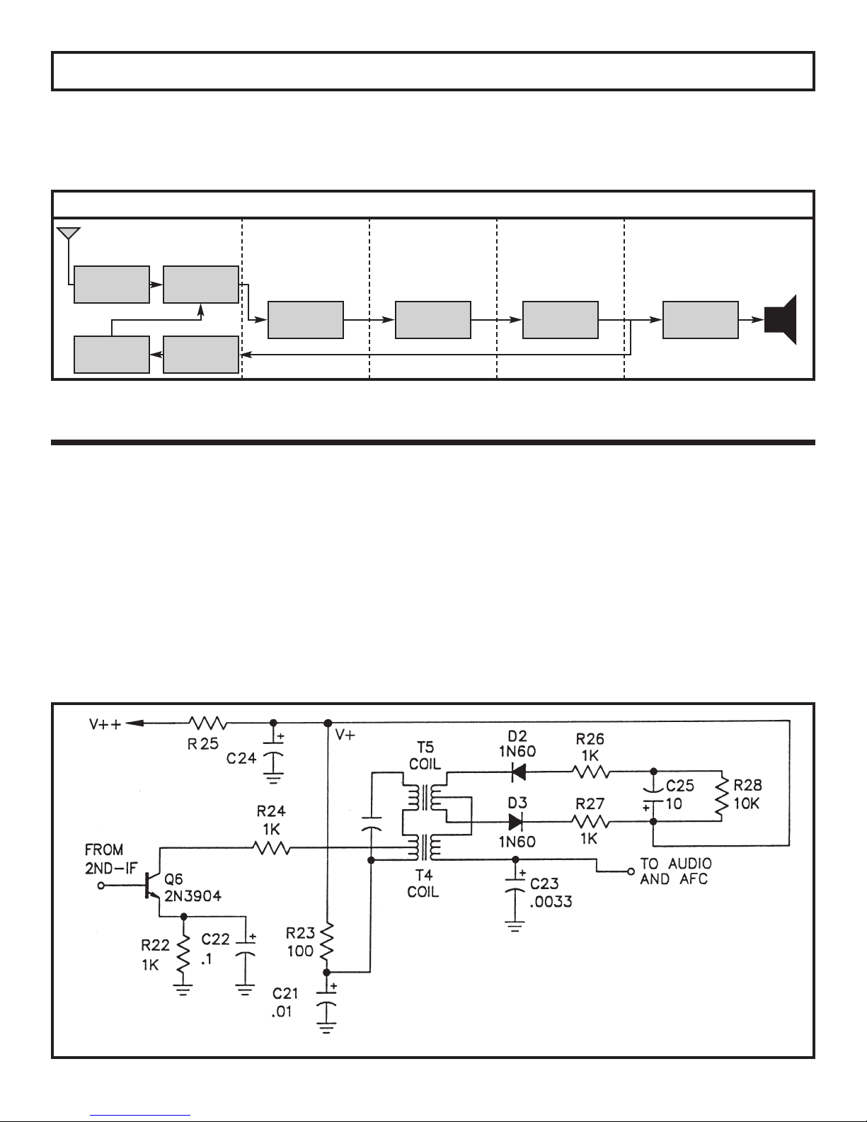
SECTION 6
THE FM RADIO
Section 6 begins the construction of the FM radio. The
stages that we will build are shown in the block diagram
below. We will begin with the FM Ratio Detector and
FM RADIO
Section 9
Section 8
Section 7 Section 6
work back to the FM Antenna. Each stage will be
tested before proceeding to the next stage.
Section 1
FM RF
AMPLIFIER
FM
OSCILLATOR
FM MIXER
1ST FM IF
AMPLIFIER
AFC
FM RATIO DETECTOR
In the AM DETECTOR section we observed that the
audio was detected from changes in the amplitude of
the incoming signal. In FM detection, the audio is
detected from changes in frequency of the incoming
signal. The RATIO DETECTOR has built-in limiting
action which limits the signal so that any noise riding on
the FM carrier will be minimized. The RATIO
DETECTOR is redrawn below for ease of explanation.
When an incoming signal is present at
current flows through D2, R26, R28, R27 and D3. At no
modulation, the current through the diodes D2 and D3
are equal because T5 is center tapped. Thus, no
T4 and T5, a
2ND FM IF
AMPLIFIER
Speaker
FM
DETECTOR
AUDIO
AMPLIFIER
current is drawn through C23 resulting in zero audio
output voltage. When the incoming signal is modulated,
the current through one diode will be greater than the
. This causes a current to flow in C23 which will
other
produce an audio voltage across C23. If the modulation
is of opposite direction than before, more current will
flow in the other diode, which will again cause current
to flow in C23 in the opposite direction resulting in an
audio v
oltage being produced across C23. The large
current drawn from the audio which causes the battery
voltage to vary. The ratio detector is decoupled further
by the resistor R23 and capacitor C21.
µF
µF
µF
µF
Figure 27
-33-
Page 35
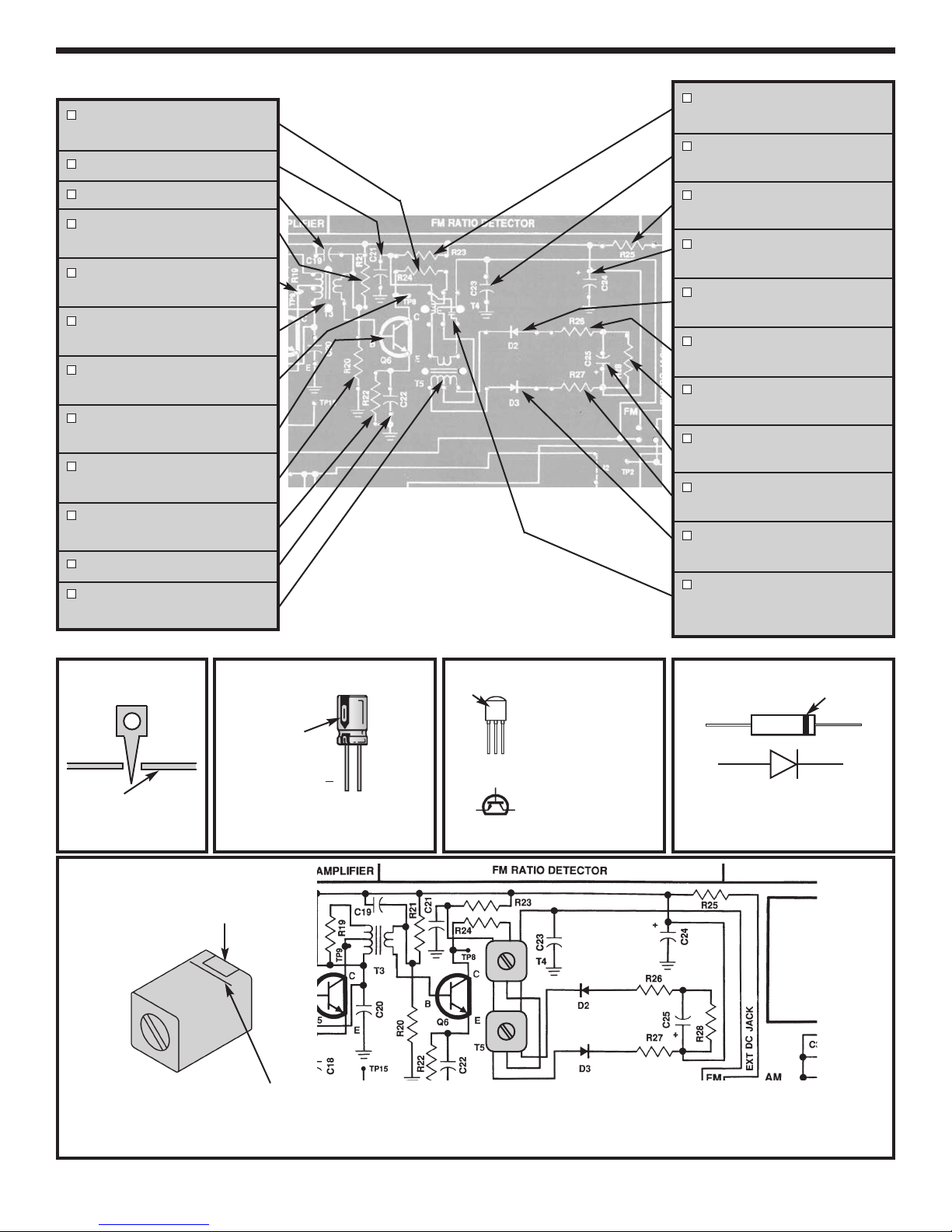
ASSEMBLY INSTRUCTIONS
R24 - 1kΩ Resistor
(brown-black-red-gold)
C21 - .01µF Discap (103)
R23 - 100Ω Resistor
brown-black-brown-gold)
(
C23 - .02µF (203)
or .022µF (223) Discap
C19 - .01µF Discap (103)
R21 - 47kΩ Resistor
(yellow-violet-orange-gold)
TP9 - Test Point Pin
(See Figure A)
T3 - FM IF Coil
(Green Dot)
TP8 - Test Point Pin
(see Figure A)
Q6 - 2N3904 Transistor
(see Figure C)
R20 - 10kΩ Resistor
(brown-black-orange-gold)
R22 - 1kΩ Resistor
(brown-black-red-gold)
C22 - .01µF Discap (103)
T5 - FM Detector Coil
(Blue Dot)
R25 - 220Ω Resistor
(red-red-brown-gold)
C24 - 470µF Lytic
(See Figure B)
D2 - 1N60 Diode
(see Figure E)
R26 - 1kΩ Resistor
(brown-black-red-gold)
R28 - 10kΩ Resistor
(brown-black-orange-gold)
C25 - 10µF Lytic
(see Figure B)
R27 - 1kΩ Resistor
(brown-black-red-gold)
D3 - 1N60 Diode
(see Figure E)
T4 - FM Detector Coil
(Pink Dot)
(see Figure 28)
Test Point Pin
Foil Side
of PC Board
Figure A
Test Point Pin
Lytic Capacitor
Polarity Mark
( )
(+)
Be sure that the negative lead is in
the correct hole on the PC board.
Figure B
NPN Transistor
Flat
Side
EBC
B
E
C
Figure C
Notch
Note: Notch m
ust be pointing to the top of the
PC board. Some FM detector coils have a red
line or part number in place of the notch.
Mount so E lead is
in the arrow hole
and flat side is in
the same direction
as shown on the
top legend.
1/4” between the
part and PC board.
Leave
Figure 28
Diode
Band
CathodeAnode
Be sure that the band is in the correct
direction.
Figure E
-34-
Page 36

STATIC MEASUREMENTS
V
Amps COM V/Ω
TP15
Figure 29
FM VOLTAGE
Connect y
AM/FM switch to the FM position.
read 9 volts DC
our VOM as shown in Figure 29. Switch the
. Turn the po
wer ON. The voltage at this
Set your VOM to
Battery
point should be betw
OFF. If you do not get this reading, check R25, C24 and
the battery v
oltage.
een 7 and 9 volts. Turn the power
TRANSISTOR CURRENT TEST
V
Amps COM V/Ω
TP15
Figure 30
VOM to the circuit as shown in Figure 30.
Connect y
Turn the power ON. The voltage at the emitter of Q6
should be about .7 v
Turn the power OFF. If your answer is greater than 2
olts
v
Since the current through resistor R22 is equal to the
our
olts. Record the voltage here:
V(Q6) = __________.
, check R20, R21, R22, R24, Q6 and the battery.
current through tr
through Q6 as follows:
Current (I) = V(Q6) / R22
Your calculated answer should be between .0005 amps
(.5 milliamps) and .0011 amps (1.1 milliamps).
ansistor Q6, calculate the current
Current (I) = __________.
YOU DO NOT HAVE AN RF GENERATOR OR OSCILLOSCOPE,
IF
SKIP TO THE RATIO DETECTOR ALIGNMENT PROCEDURE.
-35-
Page 37

DYNAMIC MEASUREMENTS
AC GAIN
The AC gain of the ratio detector is set by the AC
impedance of the primary side of T4 and the current
through Q6. The current is set by R20, R21 and R22.
Capacitors C22 and C19 bypass the AC signal to
ground. Connect your RF generator and oscilloscope
to the circuit as shown in Figure 31.
Your scope probe must have an input capacitance of
12pF or less, otherwise the probe will detune T4
causing an incorrect measurement of the AC gain. Set
the generator for 10.7MHz no modulation and minimum
voltage output. Set the scope to read 50mV/division.
Turn the power ON and slowly increase the amplitude
of the generator until 3 divisions or 150mVpp are seen
Generator
.001µF
on the scope. With an alignment tool or screwdriver,
adjust T4 for a peak. Reduce the generator input to
maintain 150mVpp on the scope. Move the scope
probe to the base of Q6 and record the voltage here:
Vb = __________ mVpp.
Turn the power OFF. The AC gain can be calculated as
follows:
AC GAIN = 150mV / Vb
Your calculated answer should be approximately 20.
Oscilloscope
Hz
TP15
Figure 31
RATIO DETECTOR ALIGNMENT
METHOD #1
ALIGNMENT WITH NO TEST EQUIPMENT
With an alignment tool or a screwdriver, turn both coils
T4 and T5 fully counter-clockwise until they stop. DO
Generator
.001µF
Hz
TP15
NOT FORCE THE COILS ANY FURTHER. Now turn
both coils in about 1 1/4 to 1 1/2 turns.
Oscilloscope
TP15
TP15
Figure 32
-36-
Page 38

METHOD #2
ALIGNMENT OF RATIO DETECTOR USING A
RF GENERATOR AND OSCILLOSCOPE
Connect the RF generator and oscilloscope to the
circuit as shown in Figure 32. Set the generator for
10.7MHz modulated at 1kHz, 22.5kHz deviation with
minimum voltage out. Turn ON the radio and turn the
volume control to the minimum. Slowly increase the
amplitude of the generator until a 1kHz sinewave is
seen on the scope. With an alignment tool or
screwdriver, peak the pink coil T4 for maximum
amplitude. Now peak the blue coil T5 for minimum
optimized. Turn the power OFF.
METHOD #3
ALIGNMENT OF RATIO DETECTOR USING A
SWEEP GENERATOR AND OSCILLOSCOPE
Connect the sweep generator and oscilloscope to the
circuit as shown in Figure 32.
for 10.7MHz and minimum v
Set the sweep generator
oltage out. Turn the po
wer
ON and set the volume control to a minimum. Increase
the amplitude of the sweep generator until an “S” curve
is seen (refer to Figure 33). Using an alignment tool or
screwdriver, adjust the blue coil T5 until the “S” curve is
centered, until each half of the “S” is equal. Now adjust
the pink coil T4 for maximum “S” amplitude. Repeat
these steps until the alignment is optimized. Turn the
power OFF.
Figure 33
SECTION 7
SECOND FM IF AMPLIFIER
The purpose of the 2nd IF amplifier is to increase the
amplitude of the intermediate frequency (IF) while also
providing Selectivity. Selectivity is the ability to “pick
out” one station while rejecting all others. T3 acts as a
bandpass filter that only passes signals around
10.7MHz. The resistor R19 is used to widen the 3dB
.707
bandwidth of the 2nd FM IF amplifier.
The gain at 10.7MHz is fixed by the AC impedance of
the primary side of T3 and the current in Q5. The
current is fixed by R16, R17 and R18. Capacitors C18
and C17 bypass the AC signal to ground. C20 is a
bypass capacitor from V+ to ground.
10.625MHz
10.775MHz
10.7MHz
Figure 34
-37-
Page 39
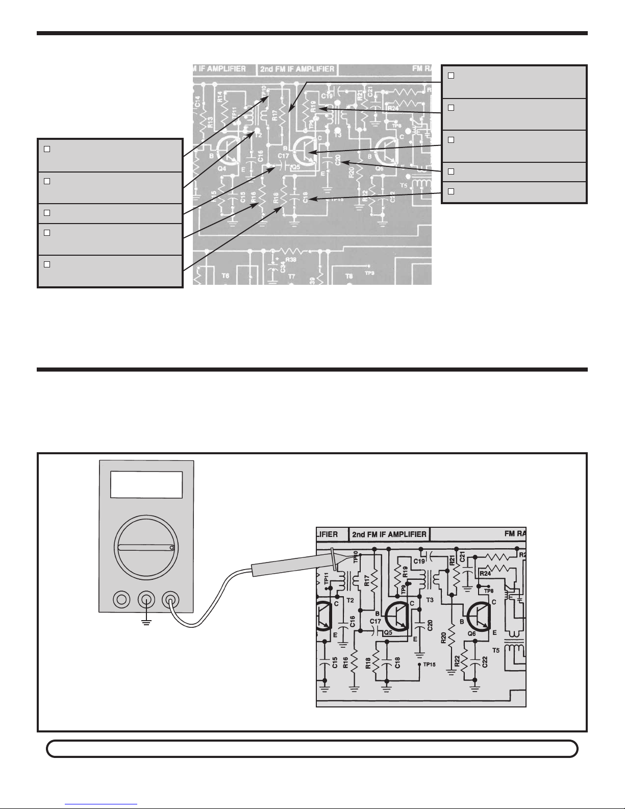
ASSEMBLY INSTRUCTIONS
TP10 - Test Point Pin
(see Figure B)
T2 - FM IF Coil
(Green Dot)
C17 - .01µF Discap (103)
R16 - 10kΩ Resistor
(brown-black-orange-gold)
R18 - 1kΩ Resistor
(brown-black-red-gold)
R17 - 47kΩ Resistor
(yellow-violet-orange-gold)
R19 - 10kΩ Resistor
(brown-black-orange-gold)
5 - 2N3904 Transistor
Q
(see Figure D)
C20 - .01µF Discap (103)
C18 - .01µF Discap (103)
STATIC TESTS
Q5 BIAS
Connect your VOM to the circuit as shown in Figure 35.
Turn the power ON. The voltage at the base of Q5
should be approximately 1.4 volts. Turn the power OFF.
V
Amps COM V/Ω
TP15
If you do not get this reading, check R17, R16, R18, Q5
and T2.
ou don’t ha
If y
ve an RF g
Figure 35
enerator and oscilloscope
-38-
skip to Section 8.
,
Page 40
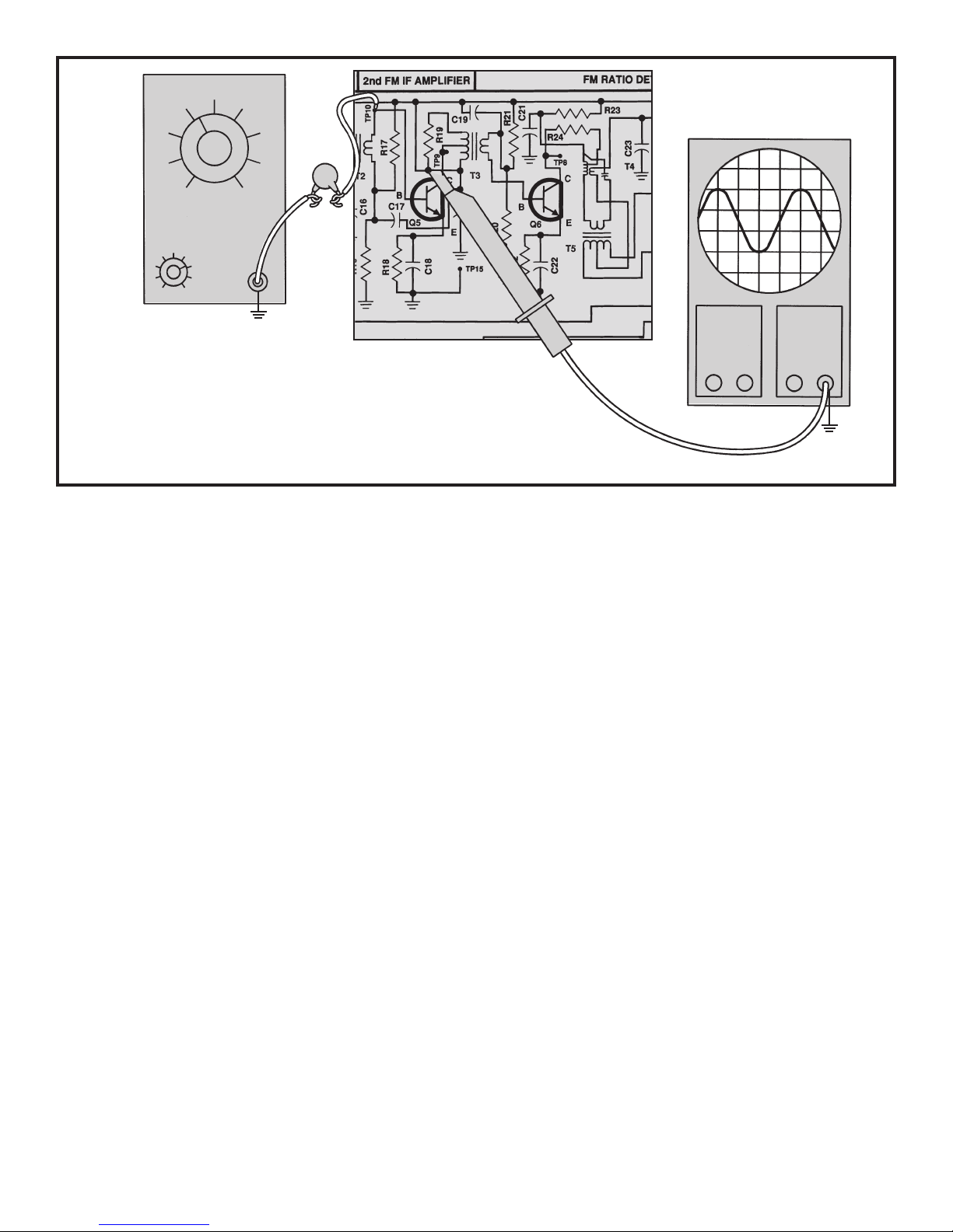
Generator
Hz
Oscilloscope
.001µF
TP15
Probe
TP15
Figure 36
AC GAIN
Connect the RF generator and oscilloscope to the
circuit as shown in Figure 36. The scope probe must
have an input capacitance of 12pF or less otherwise the
probe will detune T3 resulting in a false reading of the
AC gain.
and minimum voltage output.
50mV per division and tur
increase the generator until 150mVpp or 3 divisions are
seen on the scope. With an alignment tool or
screwdriver adjust T3 for a peak. Reduce the generator
until 150mVpp or 3 divisions are seen on the scope.
With an alignment tool or screwdriver adjust T3 for a
peak. Reduce the generator input to maintain 3
divisions on the scope. Move the probe to the base of
Q5 and record the input voltage here:
Turn the power OFF. The AC gain can be calculated as
follows:
Your calculated answer should be about 20.
Set the generator at 10.7MHz no modulation
Set the scope to read
n the power ON.
Slowly
Vb = __________ mVpp.
AC Gain = 150mV / Vb
BANDWIDTH
With the power turned OFF, connect your test
equipment as shown in Figure 36. Set your generator
at 10.7MHz no modulation and minimum voltage
output. Set the scope to read 50mV per division. Turn
the power ON and slowly adjust the generator
amplitude until 150mVpp is seen on the scope. Realign
T3, if necessar
y, for maxim
the generator to maintain 150mVpp. Slowly decrease
the frequency of the generator until the voltage drops
.707 of its original value, 2.1 divisions or 106mVpp.
Record the frequency of the lower 3dB drop-off point
here:
Fl = _________MHz.
Increase the frequency until the v
its original value, 2.1 divisions or 106mVpp. Record the
frequency of the high frequency 3dB drop-off point
here:
Fh = ___________MHz.
The bandwidth of the 2nd IF can be calculated as
follows:
um output while adjusting
oltage drops to .707 of
Record your calculation:
C Gain = __________
A
Bandwidth = Fh - Fl
our results should be betw
Y
Record y
our calculation:
-39-
een 300 - 500kHz.
Bandwidth = __________
Page 41
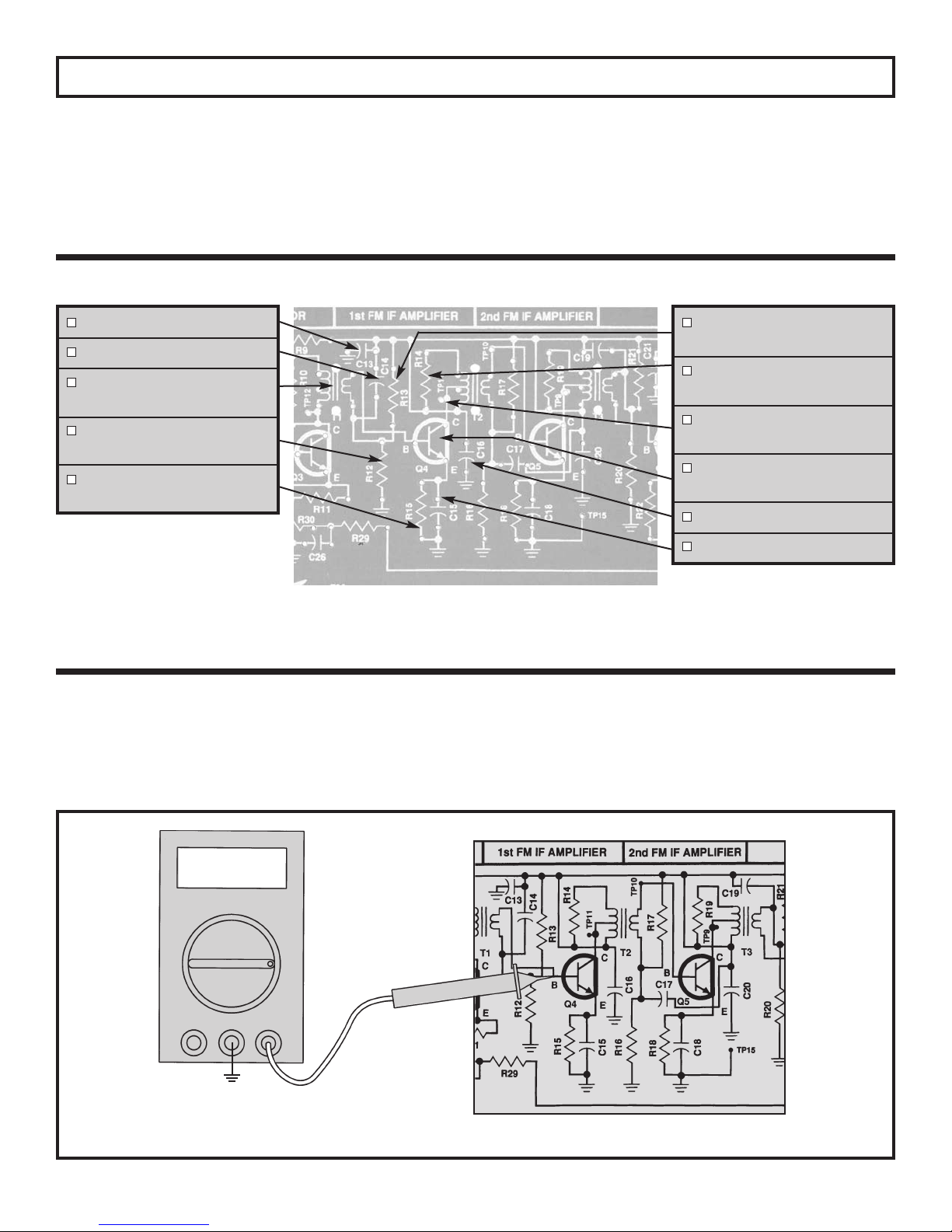
SECTION 8
FIRST FM IF AMPLIFIER
The operation of the first IF amplifier is the same as the
second IF amplifier except that the gain is different.The
gain is set by the AC impedance of the primary side of
T2 and the current in Q4. The current in Q4 is set by
the resistors R12, R13 and R15. Capacitors C14 and
ASSEMBLY INSTRUCTIONS
C15 bypass the AC signal to ground. C13 and C16 are
bypass capacitors from V+ to ground to prevent
feedback on the V+ line. R19 is used to widen the
bandwidth of the transformer T2.
C13 - .01µF Discap (103)
C14 - .01µF Discap (103)
T1 - FM Mixer Coil
(Orange Dot)
R12 - 10kΩ Resistor
(brown-black-orange-gold)
R15 - 2.2kΩ Resistor
(red-red-red-gold)
STATIC TESTS
Q4 BIAS
Connect your VOM as shown in Figure 37. Turn the
power ON. The voltage at the base of Q4 should
R13 - 47kΩ Resistor
(yellow-violet-orange-gold)
R14 - 10kΩ Resistor
(brown-black-orange-gold)
TP11 - Test Point Pin
(see Figure A)
Q4 - 2N3904 Transistor
(see Figure C)
C16 - .01µF Discap (103)
C15 - .01µF Discap (103)
approximately be 1.4 volts. If you do not get this
reading, check R12, R13, R15, Q4 and T1.
V
Amps COM V/Ω
TP15
Figure 37
-40-
Page 42

Hz
If you don’t have an RF generator and oscilloscope, skip to Section 9.
enerator
G
.001µF
Oscilloscope
TP15
Figure 38
Connect the RF generator and oscilloscope and
oscilloscope to the circuit as shown in Figure 38. The
scope probe must have an input capacitance of 12pF or
less otherwise the probe will detune T2 causing an
incorrect measurement of AC gain. Set the generator
at 10.7MHz no modulation and minimum voltage
output. Set the scope to read 20mV per division and
turn the power ON. Slowly increase the amplitude of
the generator until 3 divisions or 60mVpp are seen on
the scope. With an alignment tool or screwdriver, adjust
T2 for a peak. Reduce the generator input to maintain
3 divisions on the scope. Move the scope probe to the
base of Q4 and record the input voltage here:
Vb = __________mVpp
Turn the power OFF. The AC gain can be calculated as
follows:
.
Probe
BANDWIDTH
Connect your test equipment as sho
Set your generator at 10.7MHz no modulation and
minimum voltage output. Set the scope to read 20mV
per division. Turn the power ON and slowly increase
the amplitude of the generator until 60mVpp is seen on
the scope. Increase the frequency of the gener
the voltage drops .707 of its original v
or 42mVpp.
Record the frequency of the high 3dB drop-off point
here:
Fh = ___________MHz.
Decrease the frequency of the generator until the
voltage drops to .707 of its original value, 2.1 divisions
or 42mVpp
. Record the frequency of the low 3dB drop-
off point here:
wn in Figure 38.
alue, 2.1 divisions
TP15
ator until
C Gain = 60mV /
A
our calculated answer should be about 10.
Y
Vb
Record your calculation:
AC Gain = __________
Fl = ___________MHz.
The bandwidth of the first IF can be calculated as
follows:
Bandwidth = Fh - Fl
Your calculated answer should be between 300 500kHz.
Record your calculation:
Bandwidth = __________kHz.
-41-
Page 43
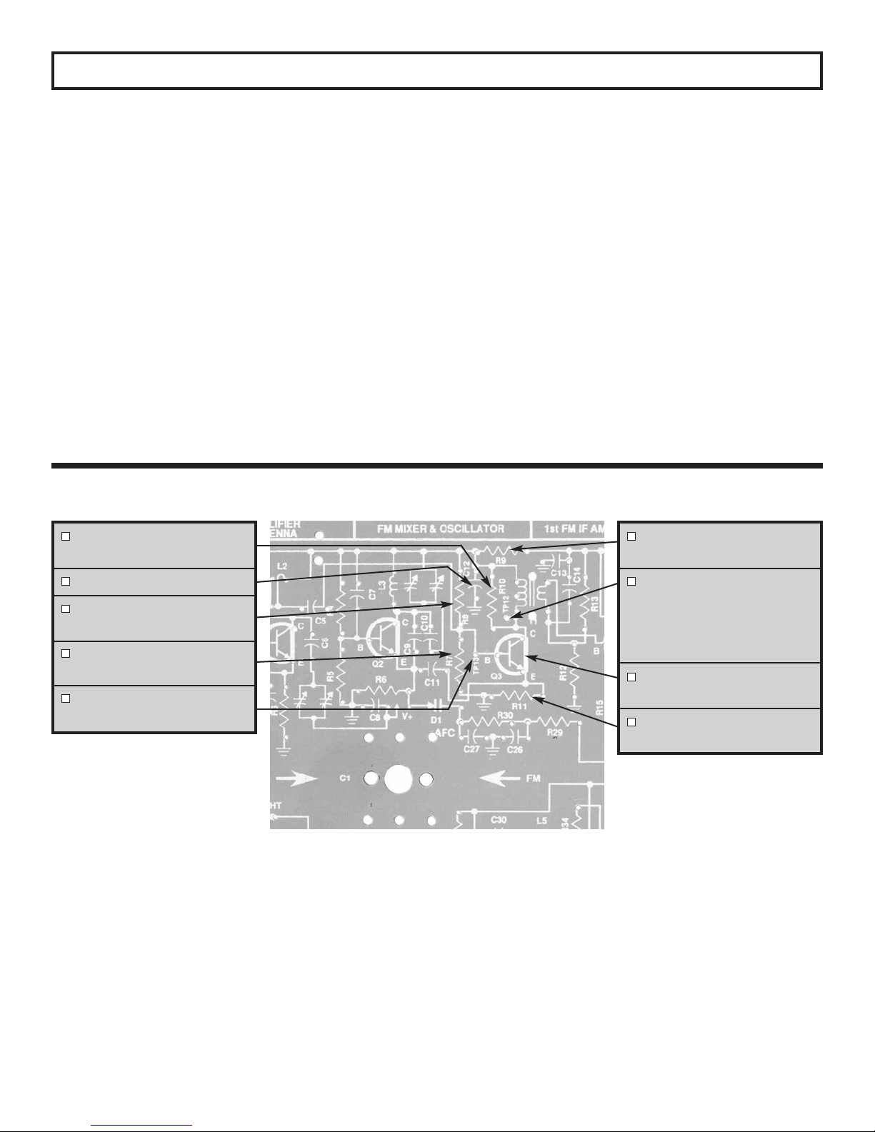
SECTION 9
FM RF AMPLIFIER, MIXER AND OSCILLATOR
In a superheterodyne receiver, the radio waves are
emitted and then mixed with the local oscillator to
produce the intermediate frequency (IF). The first stage
is the RF amplifier which selects a radio station and
amplifies it. The second stage is the local oscillator
which oscillates at a frequency 10.7MHz above the
desired radio station frequency. The third stage is the
mixer stage where the amplified radio waves are
heterodyned with the local oscillator. During the mixing
process, a difference frequency of 10.7MHz is
produced. This difference frequency is used as the IF
in FM radios. The collector of transistor Q3 contains an
IF transformer (T1) which is tuned only to the difference
frequency. This transformer rejects all frequencies
MIXER ASSEMBLY INSTRUCTIONS
except those near 10.7MHz. T1 also couples the
10.7MHz signal to the first FM IF amplifier. The RF
amplifier and the oscillator are the only two resonant
circuits that change when the radio is tuned for different
stations. Since a radio station may exist 10.7MHz
above the oscillator frequency, it is important that the
RF stage rejects this station and selects only the station
10.7MHz below the oscillator frequency. The frequency
of the undesired station 10.7MHz above the oscillator is
called the image frequency. Since this FM receiver has
an RF amplifier, the image frequency is reduced
significantly. The resistor R9 and capacitor C12
decouple the voltage of the tuner from the voltage of the
IF stages.
R10 - 10kΩ Resistor
(brown-black-orange-gold)
C12 - .005µF Discap (502)
R8 - 22kΩ Resistor
(red-red-orange-gold)
R7 - 6.8kΩ Resistor
(blue-gray-red-gold)
TP13 - Test Point Pin
(see Figure A)
R9 - 100Ω Resistor
(brown-black-brown-gold)
TP12 - Test Point Pin
(see Figure A)
CAUTION: Test Point must
not touch can of T1 FM Mixer
Coil.
Q3 - 2N3904 Transistor
(see Figure C)
R11 - 1.8kΩ Resistor
(brown-gray-red-gold)
-42-
Page 44

STATIC MEASUREMENTS
Q3 BIAS
V
Amps COM V/Ω
TP15
Figure 39
With the power turned OFF, connect your VOM to the
circuit as shown in Figure 39.
volts DC and tur
base of Q3 should be approximately 1.8 volts
answer varies by more than 2 volts, turn the power OFF
and check components R7, R8, R11 and Q3.
If you don’t have an RF generator and oscilloscope,
skip to the FM Oscillator Assembly Procedure.
n the power ON. The DC voltage at the
Set your VOM to read 9
. If your
AC GAIN
The AC gain of the mixer is set by the impedance of the
imary side of T1 and by the current flowing in Q3. The
pr
current in Q3 is set by the resistors R7, R8 and R11.
Connect your test equipment to the circuit as shown in
Figure 40. Your scope probe must have an input
capacitance of 12pF or less, otherwise the probe will
detune
your scope to read 10mV per division. Set your RF
gener
output. Turn the power ON and slowly increase the
amplitude of the generator until 4 divisions or 40mVpp
T1 resulting in an incorrect measurement.
ator at 10.7MHz no modulation minimum voltage
Set
are seen on the scope. With an alignment tool or a
screwdr
amplitude to maintain 4 divisions on the scope. Move
the scope probe to the base of Q3 and record the input
voltage here:
Turn the power OFF. The gain can be calculated as
follows:
our calculated answer should be about 3.
Y
Record your calculation:
Because the signal from the oscillator is injected at the
emitter of Q3, the emitter resistor is not bypassed to
round. This is why the gain of the mixer is low
g
compared to the other IF stages.
iver, adjust T1 for peak. Reduce the generator
Vb = __________mVpp.
AC Gain = 40mV / Vb.
AC Gain = __________
-43-
Page 45

Generator
Hz
Oscilloscope
.001µF
Probe
TP15
Figure 40
BANDWIDTH TEST
Connect your test equipment to the circuit as shown
in Figure 40. Set your generator at 10.7MHz no
modulation and minimum voltage output. Set the
scope f
or 10mV per division.
Turn the power ON and
slowly increase the amplitude of the generator until
40mVpp are seen on the scope. Increase the
frequency until the voltage drops .707 of its original
value, 2.8 divisions or 28mVpp. Record the
frequency of the generator until the voltage drops
.707 of its original value
, 2.8 divisions or 28mVpp.
Record the frequency of the low 3dB drop-off point
here:
Fl = _________MHz.
Turn the power OFF. The bandwidth can be
calculated as follows:
Your calculated answer should be between 300 500kHz.
Record your calculation:
FM OSCILLATOR ASSEMBLY INSTRUCTIONS
TP15
Bandwidth = Fh - Fl
Bandwidth = _________kHz.
C7 - .001µF Discap (102)
R4 - 33kΩ Resistor
ange-or
(or
Q2 - 2N3904 Transistor
R5 - 33kΩ Resistor
(orange-orange-orange-gold)
R6 - 2.2kΩ Resistor
C8 - .005µF Discap (502)
ange-or
(see Figure C)
(red-red-red-gold)
ange-gold)
L3 - FM Oscillator Coil
(5 Turns)
C9 - 15pF Discap (15)
C10 - 30pF Discap (30)
C11 - 220pF Discap (221)
-44-
Page 46

STATIC MEASUREMENTS
Q2 BIAS
Connect your VOM to the circuit as shown in Figure 41.
Set your VOM to read 9 volts and turn the power ON.
The voltage at the base of Q2 should be about 4
V
Amps COM V/Ω
TP15
volts. Turn the power OFF. If you do not get this
measurement, check R4, R5 and Q2.
Figure 41
AFC
When a r
desirable for the radio to “lock” in on the station. Due
to changes in temperature, voltage and other effects,
the local oscillator ma
oscillation. If this occurs, the center frequency of
10.7MHz will not be maintained. Automatic
Frequency Control (AFC) is used to maintain the
10.7MHz center frequency. When the local oscillator
drifts, the ratio detector will produce a DC
“correction” voltage. The audio signal rides on this
DC correction voltage. This signal is fed to a filter
network which removes the audio so that a pure DC
voltage is produced. This voltage is fed to a special
adio is tuned to a station, it w
y change its frequency of
ould be
AFC ASSEMBLY INSTRUCTIONS
actor. A v
diode called a v
internal capacitance when a voltage is applied. The
ratio detector diodes are positioned in such a way
that when the 10.7MHz center frequency increases
the DC correction voltage will decrease. Likewise,
when the 10.7MHz center frequency decreases, the
DC correction voltage will increase. This voltage
change causes the capacitance of the varactor to
change. The varactor is connected at the emitter of
Q2, so any capacitance change in the varactor is
seen at the emitter of the oscillator. A change in
capacitance at the emitter of Q2 will change the
frequency of oscillation of the local oscillator.
ar
aractor will change its
,
R30 - 390kΩ Resistor
w-gold)
ange-white-y
(or
Varactor Diode
D1 -
(see Figure F)
C27 - .001µF Discap (102)
ello
R29 - 390kΩ Resistor
(orange-white-yellow-gold)
C26 - .1µF Discap (104)
-45-
Page 47

If you don’t have an RF generator, skip to the RF Amplifier Assembly Procedure.
.001µF
Generator
Hz
Amps COM V/Ω
V
TP15
Figure 42
Connect the RF generator and VOM to the circuit as
shown in Figure 42. Set your VOM to read 9 volts DC.
Set your generator at 10.7MHz no modulation and
moderate signal strength output. Turn the power ON.
Record the voltage of D1 here:
V(D1) = ________.
While watching your VOM, slowly decrease the
frequency of your generator. As the frequency
decreases, the voltage at D1 should increase. Increase
RF AMPLIFIER ASSEMBLY INSTRUCTIONS
R1 - 22kΩ Resistor
(red-red-orange-gold)
C3 - .001µF Discap (102)
C2 - .005µF Discap (502)
Q1 - 2N3904 Transistor
(see Figure C)
TP15
the frequency of the generator until the voltage is equal
to V(D1). While watching your VOM, increase the
frequency of your generator. As the frequency
increases, the voltage at D1 should decrease. This
correction voltage is what keeps the oscillator from
drifting. If the voltage at D1 still does not change at D1,
check D1, R29, R30, C26 and C27. If these parts are
inserted correctly and the voltage at D1 still doesn’t
change, then increase the amplitude of your generator
and repeat the same steps again. Turn the power OFF.
L1 - FM RF Amp Coil
(6 Turns) see Figure N
L2 - FM RF Amp Coil
Turns) see Figure N
(2
C5 - 470pF Discap (471)
C6 - 33pF Discap (33)
R2 - 6.8kΩ Resistor
(blue-gray-red-gold)
C4 - 470pF Discap (471)
R3 - 470Ω Resistor
(yellow-violet-brown-gold)
TP14 - Test Point Pin
(see Figure A)
Figure N
-46-
Page 48
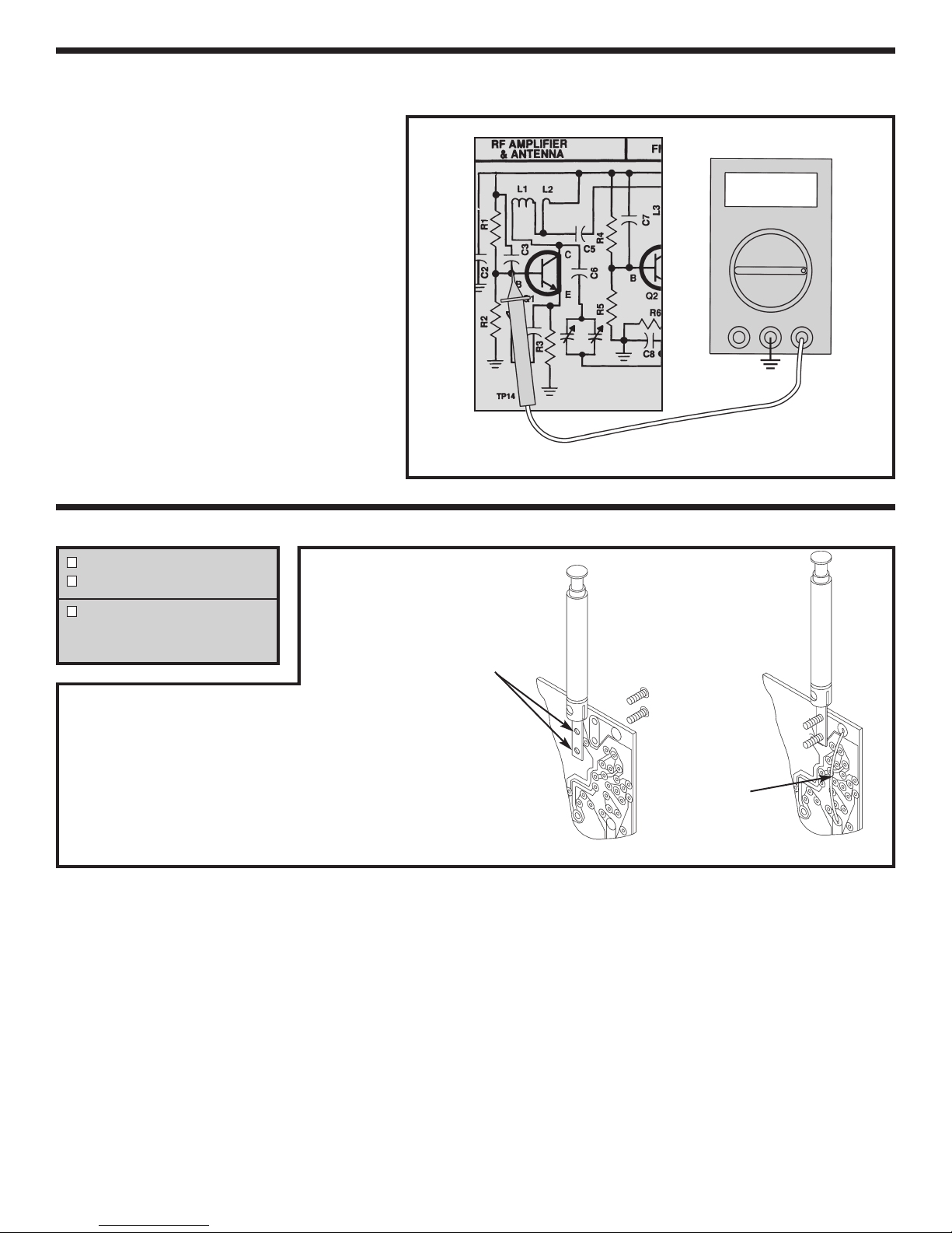
STATIC MEASUREMENTS
Q1 BIAS
Connect your VOM to the circuit as shown in
Figure 43. Set your VOM to read 9 volts and
turn the power ON. The voltage at the base of
Q1 should be about 1.6 volts. If you do not get
this reading, check R1, R2, R3 and Q1. Turn
the power OFF.
Figure 43
COM
TP15
V
V
ANTENNA FM ASSEMBLY
Antenna FM
2 Antenna Screws M2
3.5” Wire #22 Insulated
(extra wire in AM Section)
(see Figure O)
Mount the antenna to the PC board with two screws as
shown. NOTE: Some antennas have only one
threaded hole.
Cut a 2 1/4” wire and strip 1/4” of insulation off of both
ends of the remaining jumper wire. There are no holes
or the wire in this location, so tack solder the wire to the
f
pads as shown.
FM FINAL ALIGNMENTS
There are two procedures for the final alignment steps.
The first alignment procedure is for those who do not
ve test equipment and the second is for those who do
ha
have test equipment.
our “magic wand” will be used to align the FM
Y
oscillator circuit and the FM RF amplifier. When the
brass end of your “magic wand” is placed near the FM
oscillator coil L3, the coil reacts as if inductance has
been removed. Likewise, when the iron end of the
“magic wand” is placed near the coil L3, it reacts as if
inductance has been added. The same is true for the
RF coils L1 and L2. When the inductance of a resonant
Threaded Holes
Figure O
Solder
Jumper Wire
circuit is changed, the resonant frequency is changed
also.
When aligning the oscillator
, changing the resonant
frequency changes the frequency of oscillation.
Lik
, when aligning the RF amp
wise
e
, changing the
resonant frequency at which it was selective.
When aligning the oscillator and RF circuits, coils L1
and L3 will be adjusted at the low
er end of the band,
while the oscillator and RF trimmer capacitors are
adjusted at the higher end of the band. This is done so
that the RF amp tracks the oscillator properly.
-47-
Page 49
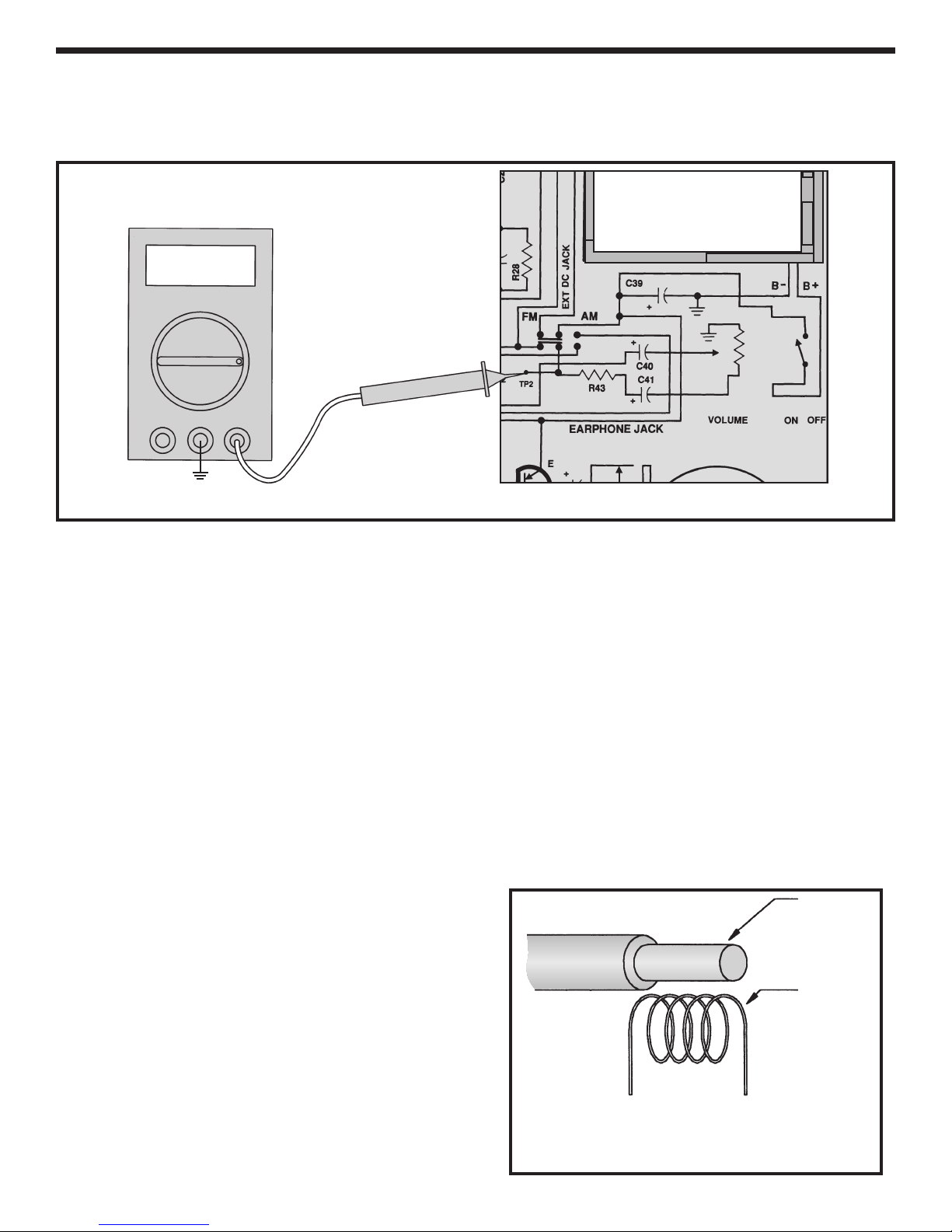
ALIGNMENT WITH NO TEST EQUIPMENT
With an alignment tool or screwdriver turn coils T1,
T2 and T3 fully counter-clockwise. DO NOT FORCE
IF ALIGNMENT
V
COM
Amps
V/Ω
THE COILS ANY FURTHER. Turn each coil in about
1 1/4 to 1 1/2 turns.
Battery
TP15
Figure 44
With an alignment tool or screwdriver turn coils T1, T2
and T3 fully counter-clockwise. DO NOT FORCE THE
COILS ANY FURTHER. Turn each coil in about 1 1/4
to 1 1/2 turns.
Use the earphone provided for best results. Switch to
the FM position. Connect your VOM to the circuit as
shown in Figure 44. Turn the radio ON and tune the
radio to a weak station. It is best to keep the volume at
a low level. Adjust T1 for the minimum voltage on your
VOM. Reduce the volume if necessary. Adjust T2 for
minimum voltage on your VOM and reduce the volume
control if necessary. Adjust T3 for minimum voltage on
your VOM and reduce the volume control if necessary.
ou adjust the coils you should hear less distortion
As y
and noise. Repeat this procedure until the FM IF gain
is optimiz
ed. This process peaked the FM IF amplifier
to their maximum gain.
DETECTOR ALIGNMENT
Adjust
for minimum distortion. Repeat these 2 steps until the
ratio detector alignment is optimized.
T4 for minimum voltage on your VOM. Adjust T5
heard, this means that L3 needs more inductance.
Carefully press together L3 until the station is heard.
Pulling apart or pressing together L3 just a small
amount will have a great effect on the coils resonant
frequency. Repeat this step until the pointer is aligned
to the station’s frequency. Tune the radio to a station
around 106MHz. Once a station is found and its
broadcast frequency is known, rotate the dial until the
white pointer is aligned with that station’s frequency on
the dial. Place the brass end of the “magic wand” near
L3. If the station is heard, it means that L3 needs more
capacitance. Carefully
(as shown in Figure L,
until the station is heard.
adjust the FM oscillator trimmer
page 23), on the back of the gang
Place the iron end of the
“magic wand” near L3. If the station is heard, it means
that L3 needs less capacitance.
Carefully adjust the
FM oscillator trimmer located on the back of the gang
until the station is heard.
“Magic Wand”
OSCILLATOR ALIGNMENT
Tune the radio to a known station around 90MHz. Once
a station is found and its broadcast frequency is known,
rotate the dial until the white pointer is aligned with that
stations frequency on the dial. Using the “magic wand”,
place the brass end near coil L3. Refer to Figure 45.
If the station is heard, this means that L3 needs less
inductance. Carefully pull apart L3 until the station is
heard.
Place the iron end near L3. If the station is
-48-
Spread apart the coil for less inductance
Press the coil together f
or more inductance
Figure 45
RF Coil
Page 50
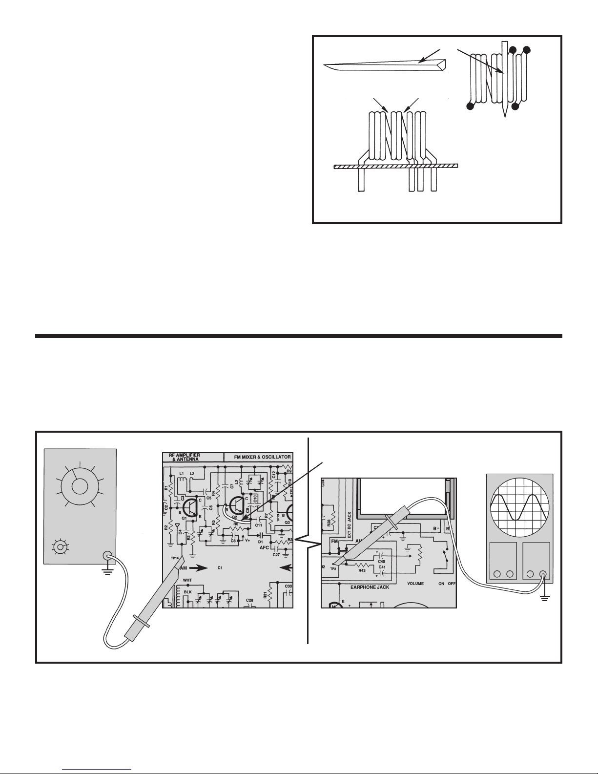
Repeat this step until the pointer is aligned to the
station’s frequency. Adjusting both the oscillator coil L3
and the oscillator trimmer capacitor will effect the
oscillator’s frequency, so it is advisable to repeat this
procedure until the FM oscillator alignment is
optimized. This process sets the FM oscillator range at
98.7MHz to 118.7MHz.
RF ALIGNMENT
Press together L1 and L2. Spread apart coil L1 so that
it resembles Figure 46. The gaps or spaces should be
between 1/32” and 1/16” wide. This procedure sets the
tracking of the RF section. Use the special coil spacer
provided to gap the coil as shown. Carefully slide the
coil spacer between the coils to get the spacing shown
in Figure 46.
This concludes the alignment of the FM radio section. If
no stations are heard, verify that FM signals are present
in your location by listening to another FM radio placed
near the superhet 108. If the FM section is still not
receiving go back and check each stage for incorrect
values and for poor soldering.
Approx.
1/16” gap
Approx.
1/16” gap
L1 L2
Figure 46
Spacer
L1
L2
Top View
ALIGNMENT WITH RF GENERATOR AND OSCILLOSCOPE
IF ALIGNMENT
Switch to the FM section. Connect your RF generator
and oscilloscope to the circuit as shown in Figure 47.
Set your RF generator at 10.7MHz modulated at 1kHz
deviation with minimum voltage output. Set the scope
Generator
Hz
TP15
to read 50mV per division. With a clip lead, short the
base emitter junction of Q2. This short “kills” the local
oscillator.
Short the base of Q2 to the
emitter (as shown below).
Battery
Oscilloscope
TP15
Turn the power ON. Slowly increase the amplitude of
the generator until a 1kHz signal is seen on the scope.
eep the generator at a low level of output to prevent
K
the IF sections from limiting. With an alignment tool or
, adjust
er
iv
wdr
scre
T1 for a peak on the scope. Reduce
Figure 47
the amplitude of the input signal if necessary. Adjust T2
for a peak and reduce the amplitude of the input signal
if necessar
is optimized. This procedure aligns the FM IF amplifiers
to 10.7MHz.
-49-
y. Repeat these steps until the IF alignment
Page 51

OSCILLATOR ALIGNMENT
Remove the clip lead and set your generator at 88MHz
modulator at 1kHz, 22.5kHz deviation and minimum
voltage output. Tune the radio until a 1kHz signal is
seen on the scope. It may be necessary to increase the
amplitude of the generator. Rotate the dial until the
white pointer is aligned to 88MHz. Using the “magic
wand” place the brass end near L3 as shown in Figure
45. If the signal seen on the scope increases, this
means L3 needs less inductance. To remove
inductance, carefully spread apart coil L3. Pulling apart
or pressing together coil L3, a small amount will have a
great effect on the coil’s resonant frequency. Place the
iron end of the “magic wand” near L3. If the signal seen
on the scope increases, it means L3 needs more
inductance. To add inductance carefully press together
coil L3. Repeat these steps until the signal decreases
for both ends of the “magic wand”. Increase the
frequency of your generator to 108MHz. Tune the radio
until a 1kHz signal is seen on the scope. Rotate the dial
until the white pointer is aligned to 108MHz. Place the
brass end of your “magic wand” near L3. If the signal
on the scope increases, it means that L3 needs more
capacitance. Adjust the FM oscillator trimmer on the
gang (as sho
signal is at a peak. Place the iron end of the “magic
wand” near L3. If the signal increases, it means that
coil L3 needs less capacitance. Adjust the FM oscillator
trimmer on the gang until the 1kHz signal is at a peak.
Repeat these 2 steps until the signal decreases for both
ends of the “magic w
oscillator coil L3 and the oscillator trimmer will effect the
frequency of oscillation, it is advisable to repeat this
procedure until the oscillator alignment is optimized.
This process sets the FM oscillator range at 98.7MHz
to 118.7MHz.
wn in Figure L on page 23) until the 1kHz
and”. Since adjusting both the
RF ALIGNMENT
Set your generator at a frequency around 90MHz
modulated at 1kHz, 22.5kHz deviation and minimum
voltage out. Tune your radio until a 1kHz tone is heard.
Place the brass end of your “magic wand” near RF coil
L1. If the signal on the scope increases, it means that
coil L1 needs less inductance. Carefully spread apart
the coil L1 to reduce its inductance. Place the iron end
of the wand near L1. If the signal increases, it means
that coil L1 needs more inductance. Carefully press
together the coil L1 to increase its inductance. Repeat
these steps until the signal on the scope decreases for
both ends of the “magic wand”. Increase your
generator to a frequency near 106MHz. Tune your
radio until a 1kHz tone is heard. Place the brass end of
your “magic wand” near L1. If the signal increases, it
means that the coil L1 needs more capacitance. With
an alignment tool or screwdriver, adjust the FM antenna
trimmer (see Figure L on page 23). If the signal
increases, this means coil L1 needs less capacitance.
Carefully adjust the FM antenna trimmer until a peak is
seen on the scope. Repeat these steps until the signal
on the scope decreases for both ends of the “magic
wand”. Since adjusting both the RF coil L1 and the
antenna tr
advisable to repeat this procedure until the RF amplifier
alignment is optimized. This process sets the RF stage
to “track” the FM oscillator stage.
This concludes the alignment of the FM radio section.
If no stations are heard, ver
present in your location by listening to another FM r
near the Superhet 108. If the FM section is still not
receiving, go back and check each stage for incorrect
values and for poor soldering.
immer will effect the gain of th RF stage, it is
ify that FM signals are
adio
FM RADIO HIGHLIGHTS
1. The FM broadcast band covers the frequency
range from 88MHz to 108MHz.
2. FM signals are usually limited to line a sight.
Audio signals up to 15kHz are transmitted on the
3.
FM carrier.
4.
The amount that the RF carrier changes frequency is
mined by the amplitude of the modulating signal.
deter
5. The number of times the carrier frequency changes
in a period of time is exactly equal to the audio
frequency.
The change in frequency is called the de
6.
is limited to 75kHz for monaural FM.
7. The bandwidth assigned for FM is 200kHz.
-50-
viation and
Page 52

DC VOLTAGES
The voltage readings below should be used in troubleshooting the FM section. (Switch at FM position.)
Q1 B 1.6 Q4 B 1.3
E .9 E .7
C 7.0 C 7.5
Q2 B 3.3 Q5 B 1.3
E 3.0 E .6
C 7.1 C 7.5
Q3 B 1.6 Q6 B 1.2
E 1.3 E .6
C 7.0 C 6.6
1. Volume set to minimum.
2. Connect TP14 to TP15 with a jumper wire.
3. Battery voltage = 9V
4. All voltages are referenced to circuit
common.
5. Voltage readings can vary +
Test Conditions
10%
SPECIFICATIONS
Audio:
Frequency response 3dB drop into 8 ohm resistive load.
Low end 800Hz - high end 120kHz
Maximum power out at 10% total harmonic distor
500 MilliWatts
Typical audio gain at 1000Hz: 150 times
Typical % distortion at 100 milliwatts output <2%.
tion.
AM Radio Specifications:
Tuning range - 520kHz to 1620kHz
IF frequency 455kHz
Tracking = +
10dB signal to noise at 200 microvolts typical
3dB from 700kHz to 1400kHz
FM Radio Specifications:
Tuning range = 88MHz to 108MHz
IF frequency 10.7MHz
Tracking +5dB from 90MHz to 106MHz
10dB signal to noise at 12 micro
Uses ratio detector and full time auto frequency control.
volts typical
-51-
Page 53

QUIZ - FM SECTION
INSTRUCTIONS: Complete the following examination, check your answers carefully.
1. The FM broadcast band is . . .
A) 550 - 1,600kHz.
B) 10.7MHz.
C) 88 - 108MHz.
D) 98.7 - 118.7MHz.
2. The maximum audio frequency used for FM is ...
A) 7.5kHz.
B) 15kHz.
C) 20kHz.
D) 10.7MHz.
3. The frequency of the modulating signal
determines the . . .
A) number of times the frequency of the
carrier changes per second.
B) maximum deviation of the FM carrier.
C) maximum frequency swing of the FM
.
ier
carr
D) amount of amplitude change of the FM
carrier.
4. The AFC circuit is used to ...
A) automatically hold the local oscillator on
frequency.
B) maintain constant gain in the receiver to
prevent such things as fading.
C) prevent amplitude variations of the FM
carrier.
automatically control the audio
D)
frequencies in the receiver.
5. The r
atio detector transf
A) 10.7MHz.
B) 88MHz.
455kHz.
C)
D) 10.9MHz.
ormer is tuned to ...
6. The ratio detector is used because ...
A) it is sensitive to noise.
B) it is insensitive to noise.
C) it provides amplification.
D) it doesn’t need a filter.
7. The device most often used for changing the
local oscillator frequency with the AFC voltage is
a ...
A) feedthrough capacitor.
B) variable inductor.
C) varactor.
D) trimmer capacitor.
8. The capacitance of a varactor is determined by ...
A) the voltage level.
B) the amount of current in the circuit.
C) the signal strength of the RF carrier.
the amount of resistance in the circuit.
D)
Limiting in FM receivers is the process of ...
9.
A) removing interfering FM stations.
B) providing greater station selectivity.
C) separ
D) removing noise from the FM carrier.
10. A detector circuit that does not require a limiter is
a ...
A) slope detector
B) ratio detector.
C) Travis detector.
D)
ating the FM stations from the AM
stations.
.
Foster-Seeley detector
.
Answers: 1. C, 2. B, 3. A, 4. A, 5. A, 6. B, 7. C, 8. A, 9. D, 10. B
-52-
Page 54

AM/FM-108T RADIO BAFFLE
OTICE:Keep the box the kit came in. After you have completed the radio and it operates satisfactorily, you may want to install a baffle
N
to improve the sound.
The final step in the radio kit will be to assemble and attach a baffle to the speaker. You will need to remove the baffle located in the
bottom of the box. If it does not want to come out easily, use a knife to cut the holding tabs.
When a speaker is not enclosed, sound waves can travel in all directions. As a speaker moves outward, it creates positive pressure on
the air in front of it and negative pressure on the rear. At low frequencies, out of phase front and rear waves mix causing partial or total
cancellation of the sound wave. The end result is a speaker less efficient and distorted.
To eliminate the low frequency cancellation, a speaker is placed inside an enclosure. Now the front sound waves are prevented from
traveling to the back. The speaker will now compress and decompress air inside, increasing its resonant frequency and Q relative to the
free air values. This type of effectively air-tight box is called an Acoustic
Suspension.
Screw
2-56 x 1/4”
Nut 2-56
AM/FM-108T Kit Carton
Cut Off
Baffle
2. Cut off two pieces of the flap as shown
and bend the four flaps upward as
1. Start at one edge and carefully remove the baffle from
the bottom of the kit box.
3. Bend the top side upward as shown. 4. Bend the two sides upward. Attach the
three sides using scotch tape or glue
(Elmer’s, Duco Cement, or other).
shown.
brown
side
5. Bend the bottom side upward and
attach it to the other sides using scotch
tape or glue
down as shown in the figure.
. Bend one mounting flap
6.
2-56 x 1/4” Screw
2-56 Nut
Back View
Insert the baffle as shown in Step 6 . Secure into place with the 2-56 x 1/4” screw and a 2-56 nut as shown in Step 6. Secure the side
of the baffle with a piece of tape as shown in Step 7.
o make an air tight seal, place a bead of seal between the PC board and the baffle.
Optional:
T
7.
Back View
Tape
-53-
Page 55
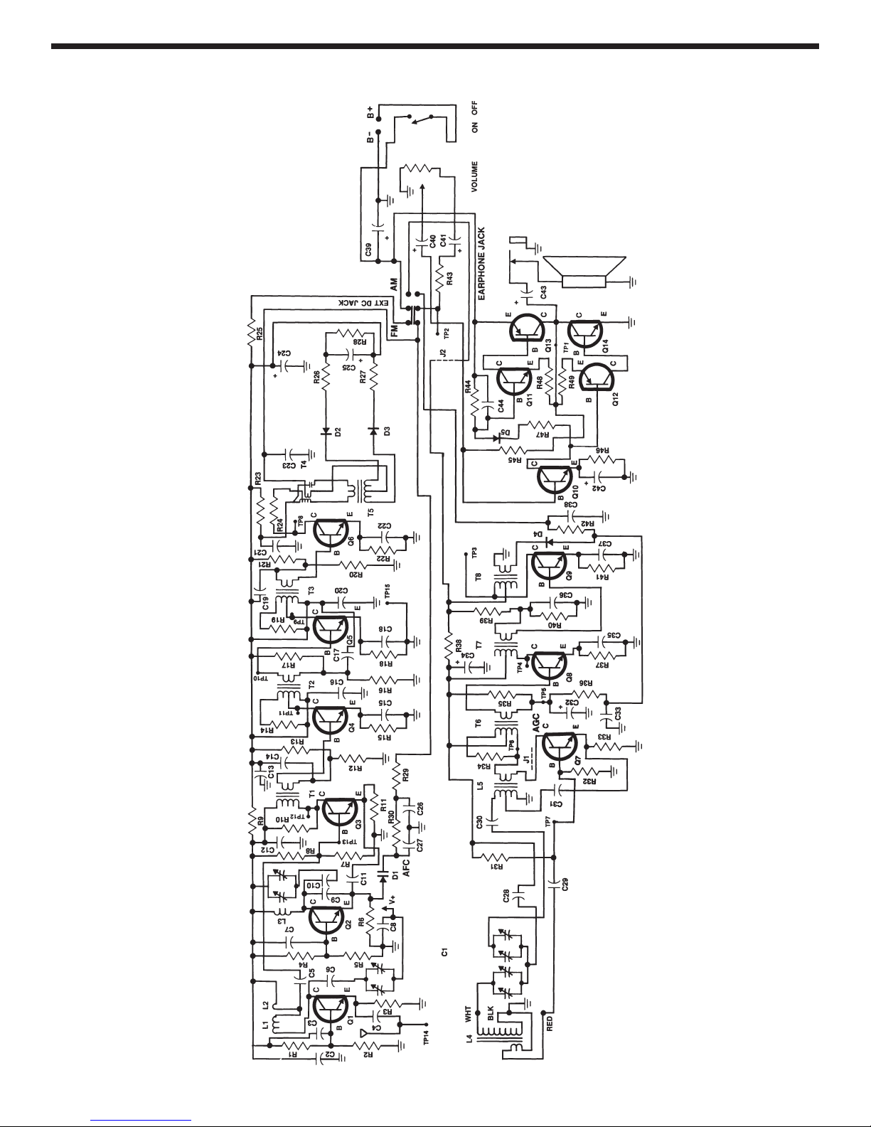
SCHEMATIC DIAGRAM - AM/FM-108T RADIO
-54-
Page 56

Elenco®Electronics, Inc.
150 Carpenter Avenue
Wheeling, IL 60090
(847) 541-3800
Website: www.elenco.com
e-mail: elenco@elenco.com
 Loading...