

Page 1
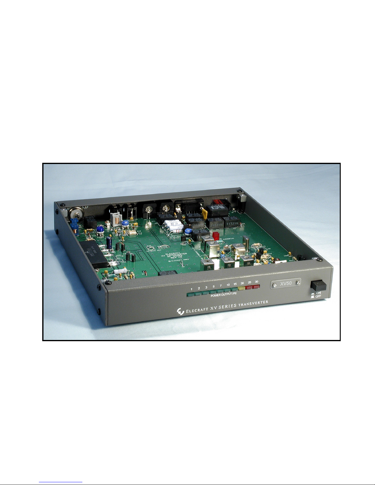
Elecraft XV Series Transverters
Models XV50, XV144, XV222
Rev B, November 7, 2003
Page 2

Table of Contents
Introduction..........................................................................................................................................................................................1
Specifications.......................................................................................................................................................................................3
Preparing for Assembly .......................................................................................................................................................................4
Parts Inventory...................................................................................................................................................................................10
Front Panel Board Assembly............................................................................................................................................................. 24
RF Board Assembly – Part I ..............................................................................................................................................................29
RF Board Assembly – Part II .............................................................................................................................................................42
RF Board Assembly – Part III ............................................................................................................................................................51
Final Assembly .................................................................................................................................................................................. 54
Alignment and Test............................................................................................................................................................................58
Installation..........................................................................................................................................................................................64
Using Your Transverter...................................................................................................................................................................... 76
Options and Modifications..................................................................................................................................................................78
Circuit Description..............................................................................................................................................................................82
Schematic and Parts Layout Diagrams……………………………………………….……………………………...……………..Appendix A
Troubleshooting...................................……………………………………………….……………………....……...………….....Appendix B
Page 3

— — 1
Introduction
The Elecraft XV Series high-performance transverters may be used with
any transceiver or transmitter/receiver pair that covers 28 MHz. Separate
transverters are offered for the following bands:
• Model XV50: 50 to 52 MHz.
• Model XV144: 144 to 146 MHz.
• Model XV222: 222 to 224 MHz
I.F. connections to the transceiver can be either single-port (single RF
cable) or dual port (separate receive and transmit cables).
The transverters include an adjustable input level control that will provide
full output from I.F. power levels from as low as 0.01 watts up to 8 watts
continuous. Full protection against accidental high-power transmit of up
to 100 watts into the I.F. port is also included.
The receiver features a very low noise figure with a PHEMT RF stage for
weak-signal work. Relays are used for transmit/receive switching to avoid
receive performance degradation by diode switches in the signal path.
The transmitter is conservatively rated at 20 watts output PEP SSB, CW
or data modes. The RF output is displayed on the front panel with a 10segment LED bargraph. The LED display may be switched between dot or
bar modes and has two brightness levels when used with an Elecraft K2
transceiver.
The transverters are housed in attractive, low-profile enclosures that may
be stacked for multi-band operation. An illuminated band label identifies
the transverter in use. Several transverters may be connected to the
transceiver in most cases. Internal relays select only the transverter for the
band in use, avoiding the need to switch I.F. cables.
Using an Elecraft K2 as the I.F. Transceiver
While the transverters will work with nearly any HF transceiver, using
them with our Elecraft K2 (or K2/100) offers additional benefits. The
high-performance K2 provides:
• Low noise, single-conversion, wide dynamic range receiver
• Four adjustable I.F. crystal filter bandwidths per mode
• Automatic transverter band switching with individual menu-
selected output power levels for up to three transverters.
• Direct display of the transverter operating frequency to 10 Hz,
including per-band adjustable offsets of +/- 9.99 kHz
• Four RIT ranges from +/- 0.6 to +/- 4.8 kHz
We recommend that K2’s with serial numbers 3445 and below be
equipped with Elecraft-approved modifications that reduce spurious
responses and enhance frequency stability. See page 68 for details.
Figure 1. Three Transverters May Be Controlled by an Elecraft K2.
Page 4

— — 2
Transverter Kits
The XV Transverters are intermediate-to-advanced kits, yet you'll be
surprised at how uncomplicated they are to build. All of the radio
frequency (RF) circuits are on one printed circuit board (PCB). A second
smaller PCB holds the microcontroller and front-panel LEDs. Highquality, double-sided PCBs are used, with plated-through holes for
optimal RF performance. Point-to-point wiring is minimal. All
components to be installed have wire leads; the few surface-mount devices
required are pre-installed on the circuit board.
This kit uses just one torodial inductor, which is easy to wind. However, if
you prefer not to wind this inductor yourself, you can order one prewound with the leads tinned and ready to install from an Elecraft-qualified
source. Ordering information is on our web site at
www.elecraft.com.
Customer Service and Support
Whether you build the kit or buy a factory-built transverter, you’ll find a
wealth of information on our web site at
www.elecraft.com. Among the
materials there you’ll find the latest application notes, photographs, any
updates to this manual, and information on new products. We also have a
popular e-mail forum, for which you can sign up from the web site. It's a
great way to interact with other Elecraft owners, exchange ideas and find
answers to many questions.
You can also get assistance by telephone or by sending an e-mail to
support@elecraft.com. E-mail is preferable because it gives us a written
record of your question. Telephone assistance is available from 9 A.M. to
5 P.M. Pacific time, Monday through Friday (except US Holidays) at 831662-8345.
Repair Service
Contact Elecraft before returning your equipment to obtain the current
information on repair fees.
To ship the unit, first seal it in a plastic bag to protect the finish. Use a
sturdy packing carton with at least 3-in (8 cm) of foam or shredded paper
on all sides. Seal the package with reinforced tape. (Neither Elecraft or the
carrier will accept liability for damage due to improper packaging.) Ship
the equipment to:
Elecraft
P.O. Box 69
Aptos, CA 95001-0069
Elecraft 1-Year Limited Warranty
If building a kit, complete the assembly, carefully following all instructions in
the manual, before requesting warranty service.
What is covered: During the first year after the date of first consumer
purchase, Elecraft will replace defective parts free of charge (post-paid). We
will also correct any malfunction caused by defective parts and materials. You
must send the unit at your expense to Elecraft. We will pay return shipping.
What is not covered: This warranty does not cover correction of assembly
errors or misalignment; repair of damage caused by misuse, negligence or
builder modifications; or any performance malfunctions involving non-Elecraft
accessory equipment. The use of acid-core solder or any corrosive or
conductive flux or solvent will void this warranty in its entirety. Also
not covered is any reimbursement for loss of use, inconvenience, customer
assembly or alignment time, or cost of unauthorized service.
Limitation of incidental or consequential damages: This warranty does not
extend to non-Elecraft equipment or components used in conjunction with our
products. Any such repair or replacement is the responsibility of the customer.
Elecraft will not be liable for any special, indirect, incidental or consequential
damages, including but not limited to any loss of businesses or profits.
Page 5

— — 3
Specifications
Numeric values are typical; your results will be somewhat different. Also,
specifications may be affected by the options or accessories chosen. See
www.elecraft.com for details about options and accessories currently
available. Specifications are subject to change without notice.
General
Size
Cabinet: 1.3” H x 7.8” W x 8.3” D
(3.3 x 19.8 x 21 cm)
Overall: 1.5 H x 7.8 W x 9.5 D incl. feet and connectors.
(3.8 x 19.8 x 21 cm)
Weight: 2.5 lbs (1.1 kg)
Supply Voltage: 13.8 VDC
Current Drain:
Receive: 250 mA (typical)
Transmit
1
: 4 A (typical)
Frequency Ranges:
XV50: 50 – 52 MHz
XV144: 144 – 146 MHz
XV222: 222 – 224 MHz
T/R Switching Time: 3 ms (typical)
T/R Key Input: Ground for transmit: must pull 5 volt
logic level to within 0.5 volts of ground
at < 1 ma.
I.F. Overload Protection: Survives 100 watts RF input at the I.F.
Port without damage with transverter
un-keyed (in receive mode).
1
Current varies with supply voltage, load impedance and power output. We
recommend a minimum 5 A supply.
Amplifier Key Output: Ground on transmit: 200 VDC at 1 A
maximum.
Connectors:
K2 Interface: DB9
Keying Line Input: RCA
Keying Line Output: RCA
I.F. In/Out: BNC
Aux (Rx-Only Ant): BNC
Antenna: SO-239 (UHF) on XVR 50
Type N on XVR 144 & XVR 222
Transmitter
Power Output: 20 watts into 50 ohms
Minimum Supply
Voltage Recommended: 12 VDC
Operating Modes: CW, SSB, AM, FM, PSK
I.F. Input Frequency Range: 28 – 30 MHz
I.F. Input Power Range: 0.01 mW (-20 dBm) to
8 watts (+ 39 dBm)
Harmonic Content: < - 60 dBc at 20 watts output.
Receiver
Noise Figure: < 1 dB
Conversion Gain: 25 dB (typical)
Image Rejection: > 60 dB
3rd-Order Intercept: +20 dBm (typical)
Page 6

— — 4
Preparing for Assembly
Overview of the Kit
The Elecraft XV transverters use modular construction, both physically
and electrically. This concept extends to the chassis (Figure 2). Any
chassis element can be removed to provide access for troubleshooting.
Figure 2. XV Transverter Modular Cabinet Parts.
There are two printed circuit boards (PCBs) in the transverter: the front
panel board, which sits vertically behind the front panel, and the large RF
board.
The boards are interconnected using board-to-board connectors which
eliminates the need for a wiring harness. Gold-plated contacts are used on
these connectors for reliability.
Tools Required
You will need the following tools to build this kit:
• Fine-tip temperature-controlled soldering station with 700 or
800°F tip (370-430°C). Do not use a high-wattage iron or gun
with small components since this can damage pads, traces, or the
parts themselves.
• IC-grade, small-diameter (.031”) solder (Kester #44 or
equivalent).
• Desoldering tools and supplies are invaluable if you make any
modifications or need to do any repairs. Narrow solder wick or a
good vacuum desoldering tool such as the Soldapullt® model
DS017LS are recommended. See Soldering, Desoldering and
Plated-Through Holes, on page 9 for more information.
i
DO NOT use acid-core solder, water-soluble flux solder,
additional flux or solvents of any kind. Use of any of these will void
your warranty.
• Screwdrivers: a small, #2 Phillips and a small flat-blade for slotted
screws.
• Needle-nose pliers.
• Small-point diagonal cutters, preferably flush-cutting.
• Digital Multimeter (DMM) for voltage checks and confirming
resistor values. A DMM with capacitance measurement capability
is desirable, but not required.
• Noise generator (Elecraft N-Gen or equivalent
2
) or signal
generator with output in the RF frequency range of the transverter.
• RF power meter capable of measuring RF power levels up to 25
watts at the RF frequency used by the transverter.
• 50-ohm dummy load capable of handling 25 watts, minimum.
Refer to www.elecraft.com for tool sources and solder recommendations.
2
Check www.elecraft.com for availability.
BACK PANEL
LEFT
SIDE PANEL
TOP
COVER
FRONT
PANEL
BOTTOM
COVER
(RIGHT SIDE
PANEL NOT
SHOWN)
.
Page 7

— — 5
Preventing Electro-Static Discharge Damage
Your XV transverter uses integrated circuits and transistors that can be
damaged by electrostatic-static discharge (ESD). Problems caused by ESD
often can be difficult to troubleshoot because components may be
degraded but still operating at first rather than fail completely.
To avoid such problems, simply touch an unpainted, grounded metal
surface before handling any such components and occasionally as you
build, especially after moving about.
For maximum protection, we recommend you take the following antistatic precautions (listed in order of importance):
1. Leave ESD-sensitive parts in their anti-static packaging until you
install them. The packaging may be a special container or
conductive foam (Figure 3). Parts which are especially ESDsensitive are identified in the parts list.
2. Ground yourself briefly before touching any sensitive parts or
wear a conductive wrist strap with a series 1 megohm resistor.
DO NOT ground yourself directly as this poses a serious
shock hazard.
3. Make sure your soldering iron has a grounded tip.
4. Use an anti-static mat on your work bench.
Figure 3. A common anti-static packaging is conductive foam which
keeps all of the terminals of a device at the same potential.
Unpacking and Inventory
We strongly recommend that you do an inventory of the parts before
beginning to assemble the kit. Even if you don’t count all the parts, an
inventory is helpful to familiarize yourself with them. A complete parts
list is included in the next section.
Identifying Parts
The parts list contains illustrations of the parts to help you identify them.
Identifying marks on the individual parts are shown in the text in
parenthesis. For example, “Transistor Q4 (PN2222)…” indicates a
transistor, Q4, which may be located in the parts list that has the
characters shown in parenthesis printed on it. Sometimes these letters are
not obvious. They may be printed in light gray on a black body, for
example. Also, there may be other marks on the device in addition to the
letters listed.
Identifying Resistors
Resistors are identified by their power capacity and their resistance value.
The power rating in watts determines the physical size of a resistor. The
most common resistors are 1/4 watt. Higher wattage resistors are
proportionately larger. The resistance value and wattage of each resistor is
shown in the Parts Lists and in the individual steps of the assembly
procedures. The silk screened outlines on the circuit boards indicate the
relative physical size of the resistors as well.
Most resistors use a color code. The color bands are listed in the text along
with the values of each resistor. For example, “R4, 100k (brn-blk-yel)…”
indicates a 100k ohm resistor and the colors to look for are brown, black
and yellow, starting with the band nearest the end of the resistor.
Some resistors use numbers instead of color bands. For example, an 820
ohm resistor might be stamped with the digits 821 instead of having gray,
red and brown color bands. Some larger resistors have their value in ohms
stamped on the body using numbers. For, example the 820 ohm resistor
would be stamped with 820 instead of 821 as described above. Normally,
when the value is shown in ohms it will be followed with the word
“ohms” or the Greek letter omega: Ω
Page 8

— — 6
Reading Resistor Color Codes
It is very helpful if you learn to read the color codes. A color-code chart
showing how to read the four-color bands on resistors with a 5% or 10%
tolerance is shown in Figure 4. 1% resistors are similar except that they
use a fifth band to provide a way of showing another significant digit. For
example, a 1,500 ohm (1.5 k-ohm) 5% resistor has the color bands brown,
green and red signifying one, five and two zeros. A 1,500 ohm (1.5 kohm) 1% tolerance resistor has the color bands brown, green, black and
brown signifying one, five, zero, and one zero.
The optional band shown in Figure 4 indicates other performance
specifications for the resistor. When used, it is separated from the other
color bands by a wider space.
i
If in doubt of a resistor’s value, use a DMM. It may be difficult to see
the colors on some resistors, particularly 1% tolerance resistors with a dark blue
body. Do NOT be concerned with minor deviations of your DMM reading from
the expected value. Typical errors in most DMMs and the tolerances of the
resistors normally produce readings that are slightly different from the value
indicated by the color bands.
Identifying Molded Inductors
Small molded inductors have color bands that use the same numeric
values as resistors but they start near the center of the inductor and work
toward the end. These colors are listed in the text after the value of the
inductor, for example: 27µH (red-vio-blk). The red stripe would be near
the center of the inductor and the black strip would be closer to the end.
On very small chokes, the first color will be only slightly farther from one
end than the last color. There may be a variety of other stripes on
inductors as well, indicating their tolerance, conformance to certain
specifications and other data.
FIRST DIGIT
TOLERANCE:
OPTIONAL
SECOND DIGIT
MULTIPLIER
Black
Brown
Red
Orange
Yellow
Green
Blue
Violet
Gray
White
Silver
Gold
0
1
2
3
4
5
6
7
8
9
-
-
X 1
X 10
X 100
X 10K
X 10K
X 100K
X 1M
-
-
X 0.01
X 0.1
COLOR
DIGIT
MULTIPLIER
GOLD = 5%
SILVER = 10%
Figure 4. Resistor Color Code.
Page 9

— — 7
Identifying Capacitors
Capacitors are identified by their value and the spacing of their leads.
Small-value fixed capacitors usually are marked with one, two or three
digits and no decimal point. The significant digits are shown in
parenthesis in the text. For example: “C2, .01 (103)”.
If one or two digits are used, that is always the value in picofarads (pF). If
there are three digits, the third digit is the multiplier. For example, a
capacitor marked “151” would be 150 pF (15 multiplied by 10
1
).
Similarly, “330” is 33 pF and “102” is 1000 pF (or .001 µF). You may
think of the multiplier value as the number of zeros you need to add on to
the end of the value.
Note: In rare cases, a capacitor manufacturer may use “0” as a
decimal placeholder. For example, “820” might mean 820 pF rather than
82 pF. Such exceptions are usually covered in the parts lists. If possible,
measure the values of all capacitor below .001 µF. Most DMMs include
capacitance measurement capability.
Fixed capacitors with values of 1000 pF or higher generally use a decimal
point in the value, such as .001 or .002. This is the value in microfarads
(µF). Capacitors also may have a suffix after the value, such as “.001J”.
The lead spacing is noted in the Parts Lists for most capacitors. If two
different types of capacitors have the same value, the lead spacing will
indicate which one to use. When the lead spacing is important, both the
value and the lead spacing is shown in the assembly procedure. For
example, “LS 0.1” means that the Lead Spacing is 0.1 in.
Hard-to-Identify Capacitor Values
2.2 pF: These are “disc ceramic” capacitors with round, pillow-shaped
bodies about 1/8” (3 mm) in diameter and a black mark on the top. The
capacitor should be labeled “2.2” but the marking sometimes requires a
magnifying glass to see clearly.
150 pF: These capacitors are marked “151” on one side, but the other side
may be marked #21ASD. The “#21” may look like “821”.
Page 10

— — 8
Assembly Process
There are seven steps in the transverter assembly process:
1. Front Panel board assembly.
2. RF Board Assembly, Part I, parts common to all models.
3. RF Board Assembly, Part II, band-specific parts.
4. RF Board Assembly, Part III, installing the RF Power
Module.
5. Final Assembly.
6. Interconnect cabling.
7. Test and alignment.
Follow the assembly process in the order given. Each part builds on what
has been completed before it. For example, the Front Panel assembly
procedure contains details about installing certain parts that are not
repeated when similar parts are installed later.
Forming Component Leads
Sometimes the space provided for a component on the PC board is larger
than the distance between the leads on the part itself. In such cases, you’ll
need to carefully bend the leads out and then down to fit the given space.
Always use long-nose pliers to accomplish this task, and bend the leads –
don’t tug on them. This is especially important with capacitor leads, which
are fragile.
Step-By-Step Procedures
Perform the assembly steps in each procedure in the order given, and
do not skip any steps. Otherwise you may find that you’ve installed
one component that hinders the installation of another. When groups
of components are installed, they are listed in a logical order as you work
around the circuit board to reduce the time needed to find where each part
goes.
Each step in the assembly procedures has a check box.
Some steps have more than one task. For example, you may be installing a
number of components listed. When a step has a number of tasks, each
task is indented with space for a check mark:
Check off each task as you complete it.
Page 11

— — 9
Soldering, Desoldering and Plated-Through Holes
CAUTION: Solder contains lead, and its residue can be toxic. Always
wash your hands after handling solder.
The printed circuit boards have circuitry on both sides (“double-sided”).
Boards of this type require plated-through holes to complete the electrical
connections between the two sides.
When you solder components on these boards the solder fills the plated
holes making excellent contact. This means that you do not need to leave a
large “fillet” or build-up of solder on top of the pads themselves. A small
amount of solder will do for all connections.
Unfortunately, removing components from double-sided PC boards can be
difficult. To remove a multi-pin component you’ll need to get all of the
solder out of every hole to free the leads. You will need to use solder wick
or a vacuum desoldering tool (see Techniques below).
The best strategy for avoiding de-soldering is to place all components
properly the first time. Double-check values, component placement and
orientation. Take care to avoid ESD damage to components.
Techniques
• Don’t pull a lead or pin out of a hole unless the solder has been
removed completely, or you are applying heat. Otherwise you can
literally pull the plating out of the plated-through hole.
• Limit soldering iron contact to a few seconds at a time.
• Use small-size solder wick, about 0.1” (2.5 mm) wide. Use wick
on both the top and bottom solder pads when possible. This helps
get all of the solder out of the hole.
• Buy and learn to use a large hand-operated vacuum desoldering
tool such as the Soldapullt® model DS017LS. Small solder
suckers are not effective.
• When removing ICs and connectors, clip all of the pins at the
body first, then remove each pin one at a time, working slowly.
You may damage pads and traces by trying to remove a
component intact, possibly leaving a PC board very difficult to
repair.
• Invest in a PC board vise with a heavy base if possible. This
makes removing parts easier because it frees up both hands.
• If in doubt about a particular repair, ask for advice from Elecraft
or someone with PCB repair experience. Our e-mail reflector is an
excellent source of help.
Page 12

— — 10
Parts Inventory
You should do a complete inventory. Contact Elecraft if you find anything missing.
i
Leave painted panels wrapped until they are needed during assembly. This will protect the finish.
Cabinet and RF circuit board components used in all transverters.
Picture Ref. Designator(s) QTY Description Part #
1
Printed Circuit Board, XV, 50,144,222
i
Handle with care – ESD Sensitive. This board is supplied with
several surface mount components pre-installed. Some of these components
are static-sensitive and are vulnerable until the other parts are installed on
the board. There is a temporary jumper across the solder pads for L1 on the
board to prevent static damage to Q3. Do not remove this jumper until
instructed to do so.
E100169
1 Front Panel E100153
1 Rear Panel E100154
2 Side Panel E100140
1 Top Cover E100146
See Figure 2.
1 Bottom Cover E100155
1 Heat Spreader E100156
8 2D Connector E100078
2 Right Angle Bracket E700073
40 Pan Head Black Machine Screw, 3/16 inch. 4-40. E700015
5 Pan Head Zinc Machine Screw, 5/16 inch, 4-40 E700077
2 Pan Head Black Machine Screw, 1/2 inch, 4-40 E700030
Page 13

— — 11
Picture Ref. Designator(s) QTY Description Part #
10 Machine Screw Nut, 4--40 E700011
14 Split Lock washer, #4 (Includes two spares) E700004
8 Internal Tooth Lock washer, #4 E700010
2 Flat Washer, #4 E700044
1 Ground Lug E700062
2 M-F Standoff for DB9 Connector E700078
4
Rubber Foot, Self Adhesive
i
A Bail kit is available as an optional accessory if desired. The
Bail will hold the front of the transverter up at a convenient viewing angle.
See www.elecraft.com for details
E980067
2 RCA Jack E620057
3 BNC Connector assy. with nut and lock washer, PC Mount E620020
3 Nut for BNC Connector E700059
3 Lock washer for BNC Connector E700058
1 DB9 Female Connector, PC Mount E620058
1 DB9 Male Cable Connector E620049
1
DB9 Back Shell (Shell components are normally packaged together in a
transparent bag).
E620050
4 Anderson Crimp Terminal E620062
Page 14

— — 12
Picture Ref. Designator(s) QTY Description Part #
1 Anderson Roll Pin E700071
2 Anderson Power Pole, Shell, Red E620059
2 Anderson Power Pole, Shell, Black E620060
P1 1 Header Connector, 12 Pin , Right Angle E620065
JP5,JP6, JP9 3 Header Connector, 2 Pin E620054
JP1,JP2,JP3,JP4, JP5,
JP6, JP9
3
7 Header Connector, 3 Pin E620007
9 Header Shorting Block, 2 Pin E620055
S2 1 DPDT Power switch E640006
SW1 1 4 Pole DIP switch E640014
1 Key Cap, Black E980023
F1 1 Resettable Fuse, 5A PolySwitch (Thin, about 3/8” [9.5mm] square.) E980065
K1, K2, K4, K5, K6, K7,
K8, K9
8
Relay, Small
(G6E-134P)
E640011
K3 1 Relay, SPDT, 12 A, 12 VDC, Large (KLT1C12DC12). E640012
D3 1 Diode, Zener, 6.8 volt, 1N5235B E560011
D5 1 Diode, SB530 E560003
D10, D11 2 Diode, LED, Red E570007
3
JP9 comprises a three pin and a two pin header connector.
Page 15
— — 13
Picture Ref. Designator(s) QTY Description Part #
Z1 1 Frequency Mixer, ADEX-10H E600050
U1 1 MMIC Amplifier, ERA-6 E600051
Pre-mounted on the
PCB
U5 1 MMIC Amplifier, MAR-3 E600073
U2 1 Voltage Regulator, 9 volt, LM78L09 E600054
Q6 1 Transistor, NPN, PN2222A E580001
U4 1 Voltage Regulator, 5 volt, LM7805 E600024
Q5 1
Transistor, MOSFET, 2N7000
i
Handle with care – ESD Sensitive. Do not remove it from its
ESD-protective packaging until you are instructed to install it.
E580002
Q4 1
Transistor, HEXFET, IRL620
E580018
Pre-mounted on
the PCB
Q3 1 Transistor, PHEMT, ATF 34143 E580020
Q2 1 Transistor, NPN , BFR96 E580021
R21 1 Resistor, metal oxide, 1 watt, 5%, 820 ohm (821) E500094
R20, R26, R27 3 Resistor, metal oxide, 3 watt, 5%,160 ohm (160) E500095
R10 1 Trimmer Potentiometer, PC mount, 100K (104) E520001
R13, R22 2 Trimmer Potentiometer, PC mount, 100 ohm (101) E520008
D1, D2, D4, D13, D6,
D12, D9, D14, D15, D16
10 Diode, 1N4148 E560002
D7, D8 2 Diode, 1N5711 E560004
Page 16

— — 14
Picture Ref. Designator(s) QTY Description Part #
R25 1 Resistor , 1/4 watt, 5%, 56 ohm (grn-blu-blk) E500096
R14 1 Resistor , 1/4 watt, 5%, 4.7 ohm (yel-vio-gld) E500062
R1, R7, R9, R33 4 Resistor , 1/4 watt, 5% , 10K ohm (brn-blk-org) E500015
R11 1 Resistor, 1/4 watt, 5%, 1K ohm (brn-blk-red) E500013
R18 1 Resistor, 1/4 watt, 5%, 620 ohm (blu-red-brn) E500097
R4, R5 2 Resistor, 1/4 watt, 5%, 5.6K ohm (grn-blu-red) E500007
R23, R34 2 Resistor, 1/4 watt, 5%, 100K ohm (brn-blk-yel) E500006
R40 1 Resistor, 1/4 watt, 5%, 22k ohm (red-red-org) E500090
R31 1 Resistor , Metal Film, 1/4 watt, 1%, 15.0K ohm (brn-grn-blk-red) E500112
R32 1 Resistor, Metal Film, 1/4 watt, 1%, 3.92K ohm (org-wht-red-brn) E500110
R30 1 Resistor, Metal Film, 1/4 watt, 1%, 7.50K ohm (vio-grn-blk-brn) E500111
R35 1 Resistor, Metal Film, 1/4 watt, 1%, 5.11K ohm (grn-brn-brn-brn) E500109
R16, R8 2 Resistor , 1 watt , 5%,120 ohm (brn-red-brn) E500105
R12, R19 2 Resistor, 1 watt, 5%, 180 ohm (brn-gry-brn) E500113
R15 1 Resistor 56 ohm SMD, 1206 size E500099 Pre-mounted on the
PCB
R17 1 Resistor, .02 ohm SMD, 2512 size E500100
C2,C57 2 Ceramic Capacitor, 100 pF (101) E530117
C35 1 Ceramic Capacitor, 10 pF (100) E530118
C55,C56 2 Ceramic Capacitor, 270 pF (271) E530050
C52,C54 2 Ceramic Capacitor , 150 pF (151) E530049
C53 1 Ceramic Capacitor, 18 pF (180) or (18), LS 0.2 E530088
C3, C17, C15, C7, C39 5
Ceramic Capacitor, .001
µF (102), LS 0.1
E530129
C8, C9, C10, C27, C16,
C19, C23, C20, C34,
C38, C37, C36, C63,
C22, C40, C6, C61, C62,
C64, C67, C71
21
Ceramic Capacitor, .01µF (103), LS 0.1
E530130
C65, C68, C29 3
Ceramic Capacitor, .047 µF (473), LS 0.1
E530131
Capacitors shown
are typical. Different
styles may be
supplied.
C30 1
Ceramic Capacitor, .22 µF (224), LS 0.1
E530132
C18 1 Ceramic Capacitor, 2.2 pF (2.2), LS 0.1 E530047
C70 1 Ceramic SMD Capacitor, 27 pF E530121
C72 1 Ceramic SMD Capacitor, 4.7 pF E530125
Pre-mounted on the
PCB
C25, C21, C24, C41, C32
C66, C31, C4, C84, C85
10
Ceramic SMD Capacitor, .047 µF, 50 V
E530120
Page 17
— — 15
Picture Ref. Designator(s) QTY Description Part #
C26, C60 2
Electrolytic Capacitor, 22 µF, 25 volt
E530012
L9 1
Molded Inductor, .47 µH (yel-vio-silver)
E690020
L8 1
Molded Inductor, 15 µH (brn-grn-blk)
E690012
L15,L16,L17 3 Variable Inductor, .243-.297 µH, shielded, grey plastic insert. E690025
L7 2 Ferrite Bead E980029
T1 1 Toroid Core, FT37-43 E680003
12 in.
(30 cm)
Solid Insulated Wire, #24 E760005
12 in.
(30 cm)
Red magnet wire, , #26 E760002
12 in.
(30 cm)
Green magnet wire, #26 E760004
3 in.
(7.5 cm)
Bare copper wire, , #14 E760023
5 ft.
(1.5 m)
Red/Black 2-conductor wire, #12 stranded (for DC power wiring) E760017
3 ft.
(91 cm)
4-conductor shielded cable (serial I/O cable) E760009
1 Heat sink gasket, large E100170
1 Heat sink gasket, small E100171
1 5” Hex Tuning Tool E980068
Page 18

— — 16
Front panel circuit board components.
Picture Ref. Designator(s) QTY Description Part #
1 Printed Circuit Board E100168
2 Screw, Fillister Head, 1/8 inch, 2-56 E700023
U1 1
Microcontroller PIC16F872, Programmed (packaged in foam)
i
Handle with care – ESD Sensitive. Do not remove it from its
conductive foam until you are instructed to install it.
E610014
1 IC Socket, 28 pin (packaged in foam) E620011
J1 1 Header Socket, 12 Pin E620008
D1, D2 2 Rectangular LED, Red E570007
D3 1 Rectangular LED, Yellow E570009
D4, D5, D6, D7, D8,
D9, D10,
7 Rectangular LED, Green E570008
R6, R7, R8, R9, R10,
R11, R12, R13,R14,
R15, R16, R21, R22,
R23
14 Resistor, Metal Film, 1/4 watt 120 ohm (brn-red-brn) E500022
R1 1 Resistor, Metal Film 1/4 watt, 5%, 220 ohm (red-red-brn) E500002
R2 1 Resistor, Metal Film 1/4 watt, 5%, 470 ohm (yel-vio-brn) E500003
R3 1 Resistor, Metal Film 1/4 watt, 5%, 10K ohm (brn-blk-orn) E500015
R4, R17 2 Resistor, Metal Film 1/4 watt, 5%, 100K ohm (brn-blk-yel) E500006
R25 1 Resistor, Metal Film 1/4 watt, 5%, 270K ohm (red-vio-yel) E500101
R18, R19, R20,R24 4 Resistor, Metal Film 1/4 watt, 5%, 2.2K ohm (red-red-red) E500104
R5 1 Resistor, Metal Film 1/4 watt, 5%, 1 megohm (brn-blk-grn) E500024
C4 1
Capacitor, Monolithic, .001 µF, (102), LS 0.1
E530129
C2, C3 2
Capacitor, Monolithic, .01 µF, (103), LS 0.1
E530130
C1 1
Capacitor, Monolithic, .047 µF (473), LS 0.1
E530131
D11 1 LED Light Bar, Yellow (packaged in foam) E570011
Page 19

— — 17
Picture Ref. Designator(s) QTY Description Part #
Q1,Q2,Q3,Q4,Q5,Q6 6 Transistor, NPN, PN2222 E580001
Z1 1 Ceramic Resonator, 4 MHz E660001
JP1 1 Header Connector, 2 pin E620054
1 Header Shorting block, 2 pin E620055
Page 20

— — 18
i
The remainder of the parts in your kit depend upon the band of operation. Check only the list that corresponds to your transverter.
XV50: The following parts are included only in the XV50 transverter.
Picture Ref. Designator(s) QTY Description Part #
1 Front Panel Label, XV50 E980059
Pre-mounted on the
PCB
U6 1
SGA7489, Sirenza Gain Block Amplifier (Three-lead device with tab. Two leads
and tab are soldered to the board. Center lead is not connected)
E600055
U3 1 Voltage Regulator, 9-volt, LM78L09 E600054
Q1 1 Transistor, NPN, MPS918 E580022
U7 1 RF Power Module, M57735 E600056
J1 1 SO-239 Chassis Mount Connector E620064
R24 1 Resistor, Metal Oxide, 2 watt, 5%, 56 ohm (56J) E500102
Z4 1 Resistor, 1/4 watt, 5%, 56 ohm (grn-blu-blk) E500096
R6 1 Resistor, 1/4 watt, 5%, 330 ohm (org-org-brn) E500103
C69 1 Ceramic Capacitor, LS 0.1, 10 pF (100) E530118
C14, C58, C59 3 Ceramic Capacitor, LS 0.1, 390 pF (391) E530051
C12 1 Ceramic Capacitor LS 0.1, 100 pF (101) E530117
C42,C43 2 Ceramic Capacitor, SMD, 50 V, 82 pF E530133
C44 1 Ceramic Capacitor, SMD, 50 V, 150 pF E530134
C5,C49,C50 3 Ceramic Capacitor, SMD, 50 V, 2.2 pF E530123
C48,C51 2 Ceramic Capacitor, SMD, 50 V, 10 pF E530135
C28 1 Ceramic Capacitor, SMD, 50 V, 15 pF E520127
C45,C47 2 Ceramic Capacitor, SMD, 50 V, 22 pF E530136
Pre-Mounted on the
PCB.
C46 1 Ceramic Capacitor, SMD, 50 V, 27 pF E530121
C1, C33 2 Ceramic Trimmer Cap, 5-30 pF E540001
Page 21

— — 19
Picture Ref. Designator(s) QTY Description Part #
Z3 1
Molded Inductor, .15 µH (brn-grn-silver)
E690022
L2, L3 2
Molded Inductor, .22 µH (red-red-silver)
E690028
L10,L11 2
Variable Inductor,
.198-.240 µH, Blue
E690032
L1 1
Variable Inductor,
.333-.407 µH, Grey
E690033
L12,L13,L14 3 Variable Inductor, .243-.297 µH, Shielded, Grey Plastic Insert. E690025
L3 2 Ferrite Bead E980029
Y1 1 Crystal, 22 MHz Fundamental (22.00) E660004
Page 22

— — 20
XV144: The following parts are included only in the XV144 transverter.
Picture Ref. Designator(s) QTY Description Part #
1 Front Panel Label, XV144 E980060
Pre-mounted on the
PCB
U6 1
Amplifier, MMIC, ERA-5 (Four-lead device with no tab. All four leads soldered to
board)
E600052
U3 1 Voltage Regulator, 5-volt, LM78L05 E600029
Q1 1 Transistor, NPN, MPS918 E580022
U7 1 RF Power Module, RA30H1317M E600058
R39 1 Pot, PC mount, 1K ohm (102) E520010
Z4, R29 2 Resistor, 1/4 watt, 56 ohm (grn-blu-blk) E500096
R24 1 Resistor, 1 watt, 120 ohm (brn-red-brn) E500105
R28 1 Resistor, 1/4 watt, 1K ohm (brn-blk-red) E500013
R6 1 Resistor, 1/4 watt, 470 ohm (yel-vio-brn) E500003
C14 1 Ceramic Capacitor, 0.1 LS, 33 pF (330) E530116
C12 1 Ceramic Capacitor, 0.1 LS, 10 pF (100) E530118
C13 1
Ceramic Capacitor, 0.1 LS, .047
µF (473)
E530131
C42,C43 2 Ceramic Capacitor, SMD, 50 V , 27 pF E530121
C44 1 Ceramic Capacitor, SMD, 50 V , 47 pF E530122
C5 1 Ceramic Capacitor, SMD, 50 V, 2.2 pF E530123
C48,C51, C28 3 Ceramic Capacitor, SMD, 50 V, 4.7 pF E530125
C45,C47 2 Ceramic Capacitor, SMD, 50 V, 12 pF E530126
C46 1 Ceramic Capacitor, SMD, 50 V, 15 pF E530127
Pre-mounted on the
PCB
C49,C50 2 Ceramic Capacitor, SMD, 50 V, 1 pF E530128
C1 1 Ceramic Trimmer Capacitor, 4-15 pF (Has a blue dot for identification) E540003
Page 23

— — 21
Picture Ref. Designator(s) QTY Description Part #
L2, Z3 2
Molded Inductor, .1 µH (brn-blk-silver)
E690021
L4 1
Molded Inductor, .15 µH (brn-grn-silver)
E690022
L10,L11 2 Variable Inductor,
.085-0.1µH, Orange E690023
L1 1
Variable Inductor,
.108-.132 µH, Orange
E690024
L12,L13,L14 3
Variable Inductor,
.059-070 µH, Red Plastic Insert.
E690027
Y1 1 Crystal, 116 MHz, 5th Overtone Series Resonant (116.000) E660016
J1 1 Type “N” Chassis Mount Female Connector E620069
Teflon Tubing E980075
Page 24

— — 22
XV222: The following parts are included only in the XV222 transverter.
Picture Ref. Designator(s) QTY Description Part #
1 Front Panel Label, XV222 E980061
Pre-Mounted on the
PCB
U6 1
SGA7489, Sirenza Gain Block Amplifier (Three-lead device with tab. Two leads
and tab are soldered to the board. Center lead is not connected)
E600055
U3 1 Voltage Regulator, 5-volt, LM78L05 E600029
Q1 1 Transistor, NPN, MPS918 E580022
U7 1 RF Power Module, RA30H2125M or RA30H2127M E600057
R28 1 Resistor, 1/4 watt, 5%, 1K ohm (brn-blk-red) E500013
R6 1 Resistor, 1/4 watt, 5%, 220 ohm (red-red-brn) E500002
R24 1 Resistor, 2 watt, 5%, 56 ohm (grn-blu-blk) E500102
R29, Z4 2 Resistor, 1/4 watt, 5%, 56 ohm (grn-blu-blk) E500096
C14 1 Ceramic Capacitor, LS 0.1, 22 pF (220) E530139
C12 1 Ceramic Capacitor, LS 0.1, 10 pF (100) E530118
C13 1
Ceramic Capacitor LS 0.1, .047 µF (473)
E530131
R39 1 Trimmer Potentiometer, PC mount, 1K ohm (102) E520010
C42, C43, C44, C44A,
C45, C47
6 Ceramic Capacitor, SMD, 50 V, 10 pF E530135
C5, 1 Ceramic Capacitor, SMD, 50 V, 2.2 pF E530123
C48,C51 2 Ceramic Capacitor, SMD, 50 V, 3.3 pF E530124
C46 1 Ceramic Capacitor, SMD, 50 V 12 pF E530126
C49, C50, C45A,
C46A, C47A
5 Ceramic Capacitor, SMD, 50 V, 1 pF E530128
Pre-mounted on the
PCB
C28 1 Ceramic Capacitor, SMD, 50 V, 4.7 pF E530125
C1 1 Ceramic Trimmer Capacitor, 4-15 pF (Has a blue dot for identification) E540003
L2, Z3 2
Molded Inductor, .1 µH (brn-blk-silver)
E690021
Page 25
— — 23
Picture Ref. Designator(s) QTY Description Part #
L10, L11, L4A, L19 4
Variable Inductor,
.064-.080 µH, Red
E690029
L1 1
Variable Inductor,
.041-.044 µH, Brown
E690034
L12, L13, L14 3
Variable Inductor, Shielded,
.038-.040 µH, Brown Plastic Insert
E690031
Y1 1 Crystal, 194 MHz 7th Overtone Series Resonant (194.000) E660017
J1 1 Type “N” Chassis Mount Female Connector E620069
1 in Teflon Tubing E980075
Page 26

— — 24
Front Panel Board Assembly
Place the front panel board on top of the heat spreader with the silk
screened side down as shown in Figure 5. Temporarily attach the board to
the heat spreader with a single 3/16” (4.8 mm) pan-head screw.
FRONT-PANEL PCB
SILK-SCREENED SIDE DOWN
Figure 5. Preparing Front Panel to Install Light Bar.
Prepare the leads of the yellow light bar for mounting on the board
by bending them as shown in Figure 6. Press the leads against a smooth,
hard surface and roll the roll the light bar until they are at about a 45
degree angle to the side of the light bar.
1
23
.
Figure 6. Preparing Light Bar Leads.
Position the light bar in the cutout of the board as shown in Figure 7.
Adjust the leads as necessary so they line up with the six solder pads at
the edge of the cutout. The leads will NOT pass through the solder pads.
The tips of the leads will rest just inside the top of each solder pad.
Figure 7. Installing Light Bar.
Solder the six terminals to the circuit board pads.
Remove the front panel board from the heat spreader.
Page 27

— — 25
i
The front panel board has parts on BOTH sides of the board.
Follow the instructions carefully. If parts are placed on the wrong
side of the board, it will not mate with the RF board properly or it
will not fit inside the enclosure when construction is finished. Parts
that go on the back (not silk screened) side of the board are identified
by asterisks on the silk screening.
Place the 28 pin IC socket in the holes provided on the front panel
board at the end opposite the light bar you just installed. The socket goes
on the BACK of the board (the side opposite the silk screened outline).
Orient the socket so the notch in the end is facing away from the end of
the board, as shown on the outline.
While holding the IC socket against the board, wet the tip of your
soldering iron with a very small amount of solder and then touch it a pin
and solder pad at one end of the socket to tack-solder it in place.
Tack-solder a second pin at the opposite end of the socket.
Check the IC socket carefully to ensure:
The socket is on the side of the board that is NOT silk-screened.
The notched end of the socket is on the end farthest from the end
of the board (as shown on the silk-screened outline).
The socket is against the board at both ends. If necessary, heat the
tack-soldered joints and adjust the socket so it is flush.
Solder all 28 pins of the IC socket and trim the leads. Be sure to
solder properly the two pins you tack-soldered above.
i
If your solder joints are not clean and shiny, your iron may
not be hot enough, or you may be using the wrong type of solder.
These "cold" solder joints will likely result in poor performance,
reliability problems, or component failure. You may wish to consult
our web site for additional soldering instructions and tool
recommendations.
Locate the silk screened outline for Q5 near the yellow light bar.
Install a PN2222 transistor on the BACK side of the board (the side that
is not silk screened). The transistor’s leads should protrude through the
board on the silk screened side.
Note: The wide, flat side of the transistor must line up with the flat
side of the silk screened outline on the board (See Figure 9). The
part number may be on either side of the transistor.
O
R
FLATTENED
BACK
ROUNDED
BACK
PCB OUTLINE
Figure 8. Transistor Orientation Guide.
Position the transistor on the board as shown in Figure 9 and bend
the leads to hold it in place. Solder and trim the leads as short as
possible.
A
PPROX.
3/16” (3 mm
)
SPACE
SOLDER & TRIM LEADS
Figure 9. Installing Transistors.
Page 28

— — 26
i
In the steps that follow, you'll be installing groups of
components. When working from a long list, install all of the items on
one line before moving on to the next. Arrows (⇒) appear in the list
to remind you of this order. Components may be soldered one at a
time or in groups. Leads can be trimmed either before or after
soldering. After trimming, leads should be 1/16" (1.5 mm) or less in
length.
Install six additional PN2222 transistors on the BACK side of the
board (the side that is NOT silk screened) just as you did Q1. Align the
flat side of each transistor with the outline shown on the silk screening.
__ Q6
⇒
__ Q1 __ Q7
__ Q2
⇒
__ Q3 __ Q4
Install capacitor C1, .047 µF (473) on the BACK side of the board
(the side that is NOT silk screened). Position the capacitor as shown in
Figure 10 .
INSERT LEADS UP
TO THE PLASTIC
COATING
473
BE SURE NUMBERS SHOWN IN PARENTHESIS
IN TEXT APPEAR ON BODY. THERE MAY BE
ADDITIONAL MARKINGS AS WELL.
SOLDER & TRIM LEADS
Figure 10. Installing Capacitors.
Install capacitor C4, .001 µF (102) on the BACK side of the board
(the side that is NOT silk screened).
Install ceramic resonator Z1 (4.0 MG) on the BACK side of the
board (the side that is NOT silk screened). This part may be inserted in
either direction. Like the capacitors, insert the resonator as far as the
plastic coating on the leads will allow.
Install JP1, a two-pin header connector on the BACK side of the
board (the side that is NOT silk screened) as shown in Figure 11 .
Temporarily place a shorting block on the pins to provide a finger rest
while soldering. Do not hold the solder iron on the pins more than 1
or 2 seconds. Excessive heat will melt the plastic part of the header.
SILK SCREENED SID
E
SHORT PINS GO
THROUGH
BOARD
Figure 11. Installing Header Connectors.
Check to ensure that:
_ All of the above parts were installed in the BACK of the
BOARD (the side with NO silk-screening).
_ All parts are soldered.
_ All leads are trimmed to 1/16” (1.5 mm) or less.
Page 29

— — 27
i
The remaining parts will be installed on the FRONT of the
circuit board
Follow the LED installation instructions carefully to preserve the
appearance of your transverter’s front panel. When finished, the
LEDs should be perpendicular to the board and in a straight line (See
Figure 12).
Figure 12. Power LEDs Installed on Front Panel Board.
Sort the rectangular LEDs into groups according to color.
Note that one lead of each LED is longer than the other. This is the
anode lead. It must be inserted in the right hand hole for each LED as
shown on the front panel board. The right hand holes have square
PCB pads to help identify them. The LEDs will not illuminate if the
leads are reversed.
Insert the leads of a green LED through the holes provided for D10
on the silk screened side of the front panel board. Be sure the long lead is
in the right-hand hole (with the square pad). Do not solder yet.
Hold the LED with the back of the plastic housing flat against the
board (not tilted). Bend the leads outward on the bottom side to hold it in
place.
Solder one lead of the LED, keeping soldering time to 1 to 2 sec.
If the LED is tilted or is not flat against the board, re-heat the lead
while pressing the LED down.
Once the LED is correctly positioned, solder the other lead, again
keeping soldering time to 1 or 2 seconds. Then trim both leads.
Install a green LED at D9. Make sure the long lead is to the right
as shown on the board. Before soldering, adjust the LED's position as
with D10.
Install green LEDs at D8, D7, D6, D5, and D4. Make sure the long
lead is to the right for these and all remaining LEDs.
Install a yellow LED at D3.
Install red LEDs at D2 and D1.
Page 30

— — 28
Sort all of the resistors by value. If the color bands are difficult to
read, use a DMM (digital multimeter) to verify their values. Tape them to
a piece of paper with the values labeled.
Install the resistors below on the front (silk screened) side of the
board. Align each resistor to rest against the board inside the silk screened
outline (See Figure 13). Start with R1 near the light bar end of the board.
__R1, 220 ohm (red-red-brn)
⇒
__R16, 120 ohm (brn-red-brn)
__R22, 120 ohm (brn-red-brn)
__R21, 120 ohm (brn-red-brn)
__R24, 2.2k (red-red-red)
__R2, 470 ohm (yel-vio-brn)
__R25, 270k (red-vio-yel)
__R23, 120 ohm (brn-red-brn)
__R14, 120 ohm (brn-red-brn)
__R15, 120 ohm (brn-red-brn)
__R13, 120 ohm (brn-red-brn)
__R5, 1 meg (brn-blk-grn)
__R3, 10k (brn-blk-org)
__R18, 2.2k (red-red-red)
__R20, 2.2k (red-red-red)
__R4, 100k (brn-blk-yel)
__R17, 100k (brn-blk-yel)
__R19, 2.2k (red-red-red)
__R12, 120 ohm (brn-red-brn)
__R11, 120 ohm (brn-red-brn)
__R10, 120 ohm (brn-red-brn)
__R9, 120 ohm (brn-red-brn)
__R8, 120 ohm (brn-red-brn)
__R7, 120 ohm (brn-red-brn)
__R6, 120 ohm (brn-red-brn)
BODY OF PART
AGAINST THE BOAR
D
ENSURE MARKINGS AGREE WITH
INSTRUCTIONS IN TEXT
SOLDER & TRIM LEADS
Figure 13. Installing Resistors.
Install the two capacitors listed below on the front (silk screened)
side of the board, near the outline of the 28-pin IC socket. Check each
capacitor's labeling carefully (shown in parentheses).
__C2, .01µF (103) __C3, .01 µF (103)
Inspect the board carefully for the following:
All connections soldered.
No solder bridges between pads (use a magnifier as needed).
All leads clipped to no more than 1/16” (2 mm) long.
Uninstalled Components
Verify that all component locations on the front panel board are
filled, except the following:
U4 (controller 16F872) should not be installed in its socket yet.
J1 at the bottom center of the board. This will be installed in the next
section.
You’ve finished the Front Panel Board Assembly Procedure. Go to the
RF Board Assembly – Part I on the next page to continue.
Page 31

— — 29
RF Board Assembly – Part I
RF circuit assembly is divided into three parts:
Part 1: DC, control circuits and RF components common to all of the
transverters.
Part 2: Additional RF components unique to each band.
Part 3: Installation of the RF power module.
i
Handle the RF board carefully. Some surface-mounted components are
used in the RF circuits for optimum transverter performance. The RF circuit
board is supplied with these components pre-mounted. Take care not to damage
them.
i
Do NOT remove the temporary wire jumper across the solder pads
for L1 until instructed to do so. This jumper protects U1 from static damage
until the circuits are completed.
Locate the two small L-brackets. Identify the shorter side of the "L",
which will be attached to the RF board.
On the RF board, locate the hole at either end of the silk screened
lettering:
P1 MOUNTS ON OTHER SIDE OF BOARD. These are the holes
where “L” brackets will be installed.
Secure the shorter leg of an L-bracket loosely to the RF board in
each hole using a 4-40 x 3/16” (4.8 mm) black screw. A lock washer is
not required at this time.
Locate the 12-pin female connector (J1) and the 12-pin male
connector (P5). Normally J1 is included with the Front Panel board parts
and P5 is with the RF Board parts.
Slide the 12-pin female connector (J1) onto the pins of the 12-pin
male connector (P1). There should be no gap between them.
Insert P1's right-angle pins into the holes on the bottom of the RF
board near the letters:
P1 MOUNTS ON THIS SIDE OF BOARD. Do not
solder yet.
Position the Front Panel board as shown in Figure 14. The pins of
J1 should be inserted into the holes in the Front Panel board, and the two
L-brackets should be aligned with their outlines on the back of the Front
Panel board.
Secure the L-brackets loosely to the Front Panel using two 4-40 x
3/16" (4.8 mm) screws (black). It is not necessary to use lock washers at
this time.
Adjust the L-bracket positions so the Front Panel board is aligned
with the RF board If the gap between the Front Panel board and the RF
board is wider at one end than the other, you probably have one of the
brackets in backwards. Be certain the shorter legs are attached to the RF
board.
P1
Top of RF board
J1
Figure 14. Installing J1 and P1.
Tighten all four L-bracket screws.
Solder all pins of J1 and P1.
Remove the two screws holding the Front Panel board to the
brackets. Unplug the Front Panel board and set it aside in a safe place.
Remove the brackets and screws from the RF Board and set them
aside.
Page 32

— — 30
Sort the fixed resistors by wattage and value as follows:
Divide the resistors by wattage: 3-watt (physically largest), 1-watt
and 1/4 watt (smallest).
Among the 1/4 watt resistors, separate the four 1% tolerance
resistors. These resistors have five color bands: four color bands
show the value plus a brown color band at one end that is wider
than the others. The wide band indicates that it is a 1% tolerance
resistor.
Sort the remaining 1/4 watt resistors by value. If the color bands
are difficult to read, use a DMM (digital multimeter) to verify
their values. Tape them to a piece of paper with the values
labeled.
Place the circuit board with the silk screened side up and the cutout
to your left. The lettering in the center of the board will read right side up.
All of the remaining parts will be installed on the top, silk screened side
of the board.
i
Save the longer clipped leads from the following resistors.
You will use several of them to make jumpers and test points later.
Install the 1-watt resistors listed below. Space each resistor about
1/16” (1.5 mm) above the board by placing the long end of one of the
right-angle brackets between the resistor and circuit board until the
resistor is soldered in place (See Figure 15). The objective is to leave
space for air to flow around the resistor. These resistors that should be
spaced above the board are shown by a double silk screen outline.
R12, 180 ohm (brn-gry-brn), near U1 in the upper left area of the
board.
R16, 120 ohm (brn-red-brn) next to R12.
R21, 820 ohms (821), 1 watt next to Q6.
R19, 180 ohm (brn-gry-brn), near U5 at the center of the board.
R8, 120 ohm (brn-red-brn) near Z1 in the lower right area of the
board.
PLACE RIGHT-ANGLE BRACKET
UNDER EACH RESISTOR UNTIL
IT IS SOLDERED IN PLACE
SOLDER & TRIM LEADS
Figure 15. Spacing the 1-watt and 3-watt Resistors above the PCB.
Install the following 3-watt resistors above R21 near the center of
the board. Space each resistor about 1/16” (1.5 mm) above the board just
like you did for the 1-watt resistors.
__R20, 160 ohm (160)
⇒
__R26, 160 ohm (160)
__R27, 160 ohm (160)
Install the 1/4-watt 1% tolerance resistors listed below in the lower
left area of the circuit board. Place these and all of the rest of the resistors
directly against the circuit board.
R35, 5.11k (grn-brn-brn-brn)
R31, 15.0k (brn-grn-blk-red)
R30, 7.5k (vio-grn-blk-brn)
R32, 3.92k (or-wht-red-brn)
Page 33

— — 31
Install the 1/4 watt resistors listed below. Start with R1, which is on
the left side just above the cutout in board. The locations follow the
perimeter of the board going clockwise.
__R1, 10k (brn-blk-org)
⇒
__R11, 1k (brn-blk-red)
__R14, 4.7 ohm (yel-vio-gld) __R23, 100k (brn-blk-yel)
Install the 1/4 watt resistors listed below. Start with R4, which is on
the lower right above Z1. The locations follow the perimeter of the board
going clockwise.
__R4, 5.6k (grn-blu-red)
⇒
__R25, 56 ohm (grn-blu-blk)
__R5, 5.6K (grn-blu-red) __R7, 10k (brn-blk-org)
__R34 (on the right edge of the board), 100k (brn-blk-yel)
__R9, 10k (brn-blk-org) __R33, 10k (brn-blk-org)
Install the following 1/4 watt resistors next to Q6 at the center of the
board:
R18, 620 ohm (blu-red-brn)
R40, 22k (red-red-org)
Locate the silk screened space for D5 on the board near R23 in the
upper right area of the board.
i
Diodes must be oriented correctly. A black band around the
diode indicates the cathode end. Install each diode so the cathode end
goes to the square solder pad and the band is oriented to match the silk
screened outline (see Figure 16 below). If a diode has more than one
band, the widest band indicates the cathode end.
Figure 16. Circuit Board Diode Orientation Guides. The cathode
always goes to the square solder pad on the board.
Install D5 (SB530) so it is against the board and the banded end of
the diode is aligned with the banded end of the PC board outline. Save
the excess leads when you clip them.
Put the clipped leads from D5 in a safe place. Keep them separate
from the other clipped leads you are saving for test points and jumpers.
You will use the leads from D5 when you install antenna connector J1
later.
Sort the small glass diodes by type. If necessary use a strong
magnifier to read the tiny numbers printed on the glass body. Tape each
group to a piece of paper marked by the type number.
1 ea. 1N5235
2 ea. 1N5711
10 ea. 1N4148
Page 34

— — 32
Install zener diode D3 (1N5235) in the upper left quadrant of the
board near R12. Position it against the board with the banded end aligned
with the banded end of the PC board outline.
Install the two 1N5711 diodes in the lower right quadrant of the
board. Place each diode against the board with the cathode band oriented
as you did in the previous steps.
__D7 __D8
Install the 1N4148 diodes listed below. Start with D1, which is near
resistor R1 in the upper left portion of the board and work clockwise
around the board.
__D1
⇒
__D12 __D6 __D9 __D13
__D14 __D15 __D16 (In lower right quadrant),
__D2 __D4
i
In the following steps you will install molded inductors. These
inductors look much like 1-watt resistors but the color codes read
differently. The color codes on the inductors read from the center to
the end instead of from the end towards the center like resistors.
Install molded inductor L8, 15µH (brn-grn-blk) in the upper right
quadrant of the board.
Install molded inductor L9, 0.47 µH (yel-vio-silver) about half way
up the board about 2 inches (5 cm) from the right-hand edge.
Install transistor Q6 (PN2222) next to R21 near the center of the
board. Orient the transistor as shown by the silk-screened outline on the
board.
Prepare transistor Q2 (BFR96) for installation as follows:
Place the transistor over the outline on the board with the lettered
side up and note the lead lengths required to match the three
solder pad areas on the board. Trim the leads to match these
pads.
Gently bend the leads down so they make solid contact with the
board starting close to the body of the transistor. This is easily
done by pressing down on the lead with a small flat-blade
screwdriver (see Figure 17).
Figure 17. Installing Transistor Q2. Use gentle pressure with a small
screwdriver blade to form the leads.
Page 35

— — 33
Solder Q2 in place as follows:
_ Wet your soldering iron with a small amount of solder and touch
it to one lead of Q2 tack-solder it in place.
_ Check alignment of the other two leads to be sure they are over
the solder pads. If necessary reheat the tack-soldered lead and
adjust the position of the transistor.
_ Solder all three leads properly, soldering the tack-soldered lead
last. Keep your soldering time as short as possible to avoid overheating the transistor. Do not hold the iron on the leads more
than two seconds.
i
Check each capacitor's labeling carefully to ensure the values
agree with the numbers shown in parenthesis.
Install the monolithic capacitors listed below near U3 and Q6 at the
center of the board.
__C68, .047 µF(473) ⇒ __C67, .01 µF (103) __C64, .01µF (103)
__C65, .047µF (473)
__C10, .01 µF (103) __C9, .01 µF (103)
Install the monolithic capacitors listed below. With the board
oriented with the cutout to the left, start with C62 near the lower left and
work around the board clockwise to the upper right quadrant.
__C62, .01 µF (103)
⇒
__C40, .01 µF (103) __C7, .001 µF (102)
__C8, .01 µF (103)
__C3, .001 µF (102) __C63, .01µF (103)
__C6, .01 µF (103)
__C22, .01 µF (103) __C61, .01 µF (103)
__C2, 100 pF (101)
__C23, .01 µF (103) __C38, .01 µF (103)
__C27, .01 µF (103)
__C29, .047 µF(473) __C37, .01 µF (103)
__C35, 10 pF (100)
__C36, µF .01 (103) __C34, .01 µF (103)
__C39, .001 µF (102)
Install the monolithic capacitors listed below. Start with C71 on the
edge of the board in the lower quadrant and work from right to left across
the lower part of the board.
__C71,.01 µF (103) ⇒ __C15, .001 µF (102) __C16, .01 µF (103)
__C20, .01 µF (103)
__C30, 0.22 µF (224) __C17, .001 µF (102)
__C19, .01 µF (103)
__C57, 100 pF (101)
Install disc ceramic capacitor C18 (2.2) next to C17 in the lower
right area of the board.
Install the capacitors listed below in the area near the center of the
board marked
28 MHZ IF BANDPASS FILTER. The lead spacing of these
capacitors may be narrower than the hole spacing on the board. If
necessary, form the leads to avoid stress on the capacitor when they are
inserted in the board. Do not force the capacitors down against the
board. The capacitors may sit about 1/16” (1.5 mm) above the board as
shown in Figure 18 .
__C55, 270 (271)
⇒
__C54, 150 (151) __C53, 18 (180) or (18)
__C52, 150 (151)
__C56, 270 (271)
The capacitors shown are typical.
Other styles may be supplied.
Figure 18. Installing I.F. Filter Capacitors.
Page 36

— — 34
Use a discarded lead to create test point TP3. Two holes for TP3 are
directly below R17 in the upper right quadrant of the board. Bend the lead
in a “U” shape and insert it in the holes indicated with a line between
them on the board. The loop formed should rise about 1/4” (4 mm) above
the board. Solder the leads.
Use a discarded lead to create TP4 next to TP3, following the
procedure described above. Solder the leads.
Make two ground test points just like you did for TP3 and TP4. The
places on the board are indicated by ground symbols. One is directly
below the “Elecraft” label and the other is in the lower left quadrant
below U6. Solder the leads.
Remove the eight small relays (G6E-134P) from the carrier tube. If
any of the pins are bent, straighten them carefully using long-nose pliers.
i
Most likely you’ll want to use a single antenna for both transmitting
and receiving with your transverter. However, some operators use separate
transmitting and receiving antennas and separate feed lines. See Connecting
the Transverter to an Antenna System. on page 74 for more information. The
following step provides special instructions to follow ONLY if you are
building your transverter for use with SEPARATE transmit and receive
antennas.
If you are building your transceiver for separate (split-path) transmit
and receive antenna connections, do the following:
_ In the next step, cross out relay “K1”. It will not be installed.
Remove K1 from your parts and set it aside in a safe place. You
may want it later if you decide to re-wire your transverter for
single antenna operation.
_ Use discarded leads to form jumpers across W2 and W3 near the
outline for K1 as shown in Figure 19.
Figure 19. Installing W2 and W3 for split path (separate transmit
and receive antenna) operation. Do NOT Install Relay K1
Working around the board clockwise from the upper left quadrant,
place the relays at the following locations. They can only be installed one
way. Do not solder the relays yet and do not clip or bend the relay
leads.
__K1
⇒
__K8 __K9 __K7
__K4
__K5 __K6 __K2
Using a thin, hardcover book to hold the relays in place, flip the
board and book over together.
Solder just two diagonally opposite corner pins on each relay.
Turn the book back over and check each relay. If any relay is not flat
against the board, re-heat its corner pins while pressing it down against
the board.
Once all the relays are properly seated, solder the remaining pins.
Take care to locate and solder all five pins on every relay. Do not trim
the relay pins. Trimming the pins can cause mechanical stress which
may reduce the life of the relay.
i
Note that W2 and W3 are used ONLY when separate
transmit and receive antennas are used and K1 is NOT installed.
Page 37

— — 35
Install resettable fuse F1 in the space provided next to relay K9. F1
may be oriented either way. Solder and trim the leads.
Check the pins on the large relay (KLT1C12DC12). If any pins are
bent, straighten them carefully using long-nose pliers.
Install the main power relay (KLT1C12DC12) next to F1 and solder
two diagonally opposite corner pins. Check the relay to ensure it is flush
against the circuit board. If necessary, reheat the solder while pressing
down on the relay.
Solder all five pins on the main power relay. Do not trim the relay
pins. Trimming the pins can cause mechanical stress which may reduce
the life of the relay.
Install a 3-terminal header at JP1 adjacent to relay K8. Put a shorting
block over two pins of the header to provide a surface where you can
place your finger to keep it straight and against the board. While holding
the assembly, touch one of the pins on the bottom of the board with a
soldering iron to tack-solder it in place. Check to ensure that the header is
sitting vertically on the board (see Figure 11). Reheat and adjust as
necessary, then solder all three pins. Do not hold the solder iron on the
pins more than 1 or 2 seconds. Excessive heat will melt the plastic
part of the header.
Remove the shorting block from JP1.
Install the following 3-terminal headers:
JP2 next to relay K8.
JP3 next to relay K8.
JP4 near resistor R21.
JP5 near relay K6.
JP6 near relay K6.
Install JP9 next to K4 and K5. JP9 requires one 2-terminal header
and one 3-terminal header.
Install the 100 k-ohm (104) potentiometer R10 (Power Cal) in the
upper left area of the board. The center lead goes toward the beveled end
of the silk screen outline (see Figure 20).The shoulders on the leads
should touch the top of the board.
Figure 20. Installing PC Board Pots. Orient the center pin toward
the beveled end of the silk screened outline.
Spread the leads on R10 to hold it in place, then solder and trim the
leads.
Install the two 100 ohm PC board potentiometers just as you did
R10:
R13 (101) in the upper left quadrant of the board near D3.
R22 (101) below the three 160-ohm 3-watt resistors near the
center of the board.
Verify that all three terminals on each pot are soldered.
Page 38

— — 36
Install 4-pole DIP switch SW1 in the space provided in the lower left
quadrant of the board. The DIP switch may not have a notch at one end to
line up with the silk screened outline. Orient the switch so that the ON
positions are on the side with the silk screened numbers. If you aren’t
sure, use your DMM to check the orientation of the switch assembly so
there is continuity through each switch when the toggle is toward the silk
screened number on the circuit board.
Bend the leads of voltage regulator U4 (UA78M05C) to fit on the
board as shown in Figure 21. Bend the leads around the shaft of a small
screwdriver to create smooth rather than sharp bends.
USE SMOOTH BEND
Figure 21. Installing Voltage Regulator U4.
Insert U4’s leads into the holes. Secure it with a zinc 4-40 x 5/16” (8
mm) screw, #4 lock washer and 4-40 nut as shown. The metal tab on the
transistor sits directly against the metal foil on the circuit board.
Solder all three leads to U4 on the bottom side of the board and trim
them short.
Install two 22 µF, 25 VDC electrolytic capacitors near the notch on
the left side of the board. Be sure to observe polarity. The longer
positive lead goes in the square solder pad with a
+ silk screened next
to it.
__C26 __C60
Locate diodes D10 and D11. They are square, red LEDs identical to
the ones you installed on the front panel board.
Locate the positions for D10 and D11 on the board, near the center
on the right hand side. Note that the square solder pad for D10 is to the
left and the square solder pad for D11 is to the right. The diodes must be
installed turned 180 degrees with respect to each other.
Position diode D10 on the board with the long lead through the
square pad on the left and the short lead through the round pad. Position
the body of the LED directly against the board within the silk screen
outline and spread the leads under the board to hold the diode in place.
Solder one lead on the bottom of the board. Check to be sure the
LED is still positioned directly against the board. Reheat and adjust the
LED as necessary, then solder and trim both leads.
Position diode D11 on the board with the long lead through the
square pad on the right, opposite the orientation of D10. Solder and trim
the leads as you did for D10.
Locate the inductors provided for L15, L16 and L17 in the I.F.
Bandpass filter. They will have grey plastic forms visible inside the
shields. Prepare the inductors for installation as follows:
Use the inductor alignment tool to exercise the core in each
inductor. If the alignment tool fits tightly, insert it from the
bottom to avoid pushing the inductor out of the shield. Run the
core up and down through the coil to ensure it runs smoothly
(some inductors are very stiff at first) then position the core near
the top of the coil.
Check the two leads and the two tabs on the case of each
inductor. If they are bent, straighten them carefully using long
nose pliers.
Page 39

— — 37
Position each inductor on the board so that its tabs and pins protrude
through on the bottom. The inductors can be positioned either way.
Ensure that the shoulders of the tabs are against the top of the board, and
then bend the tabs toward each other until they are flat on the board to
hold the inductor in place.
__L16
⇒
__L15 __L17
Solder the two tabs and the two pins on all three inductors.
Install voltage regulator U2 (78L09) in the space provided near L17.
Be sure to align the body with the silk screen outline on the board.
Install transistor Q4 (IRF 620) in the space provided near diodes D7
and D8 as shown in Figure 19. Be sure the leads are inserted until their
shoulders are against the top of the board. If the leads are not
inserted far enough, the tab on the top of the transistor may short
against the top cover when the cabinet is assembled. Trim the leads as
short as possible on the bottom of the board.
Figure 22. Installing Transistor Q4.
i
The following transistor is particularly sensitive to electrostatic discharge (ESD) damage. If you are not wearing a grounded
anti-static wrist strap, touch an unpainted, grounded object before
handling Q5.
Install transistor Q5 (2N7000) in the space provided on the right
edge of the board.
Install two 2-pin header connectors next to Q5.
__JP8 __JP7
Page 40

— — 38
Wind torodial transformer T1 on the FT37-43 toroid core as follows4.
T1 uses a bi-filar winding, which means that two wires are wound on the
core together. The wires will be twisted together loosely before they’re
wound onto the core.
Twist the red and green enameled wires together over their entire
length. The wires should cross over each other 2 to 4 times per
inch (1 to 2 times per cm).
Wind 4 turns of the twisted pair on the FT37-43 toroid core as
shown in Figure 23. Each time the wire passes through the core
counts as one turn, so verify that the wires pass through the toroid
four times. Spread the turns around the core as shown in the
figure.
Separate the leads and trim them to a length of about 1” (2.5 cm).
Figure 23. Installing T1.
4
A pre-wound toroid is available from an Elecraft-approved source. See page 4.
i
In the next step the toroid leads will be stripped and tinned. The
leads must be prepared correctly to provide good electrical contact when
installed.
Strip the insulation and tin the leads using one of the following
techniques:
1. Heat Stripping:
a. Place a small amount of solder (a.k.a. a “blob” of solder) on
your soldering iron.
b. Insert the clipped end of the wire into the hot solder. If the
iron is hot enough, you should see the insulation bubble and
vaporize after 4 to 6 seconds.
c. Add more solder and feed more wire into the solder as the
enamel melts. Continue tinning the wire up to the edge of the
core, and then slowly pull the wire out of the solder.
d. If any enamel remains on the lead, scrape it away using your
thumbnail or sharp tool.
2. Burning: The insulation can be burned off by heating it with a
butane lighter for a few seconds. Use sandpaper to remove the
residue, then tin the bare wires.
3. Scraping: Use a sharp tool to scrape the insulation away. Work
carefully and gently: do not nick the wire. Work around the
entire circumference of the wire to remove all of the enamel and
tin the bare wires.
Page 41

— — 39
Insert the tinned leads in the holes on the board and position the
toroid as shown in Figure 23. Be sure the correct lead goes to each hole.
Use a magnifier to check the following:
Bare, tinned wire should be visible where the wire enters the
hole at the top of the board. If necessary remove the toroid and
strip the wire further to ensure the wire going through the hole is
free of enamel and tinned.
Check carefully for shorts between the wires. The toroid core is
not a conductor. Bare wire may touch the core. Be sure that the
tined wires do not touch each other.
Solder the wires on the bottom of the board and trim the leads as
short as possible.
Locate the solder pads for choke L7 on the left side of the board next
to the notch (see Figure 24) Choke L7 consists of a bare wire passing
through two ferrite beads as shown.
Figure 24. Installing L7.
Strip the insulation from 3” (7.5 cm) of the #24 solid insulated wire
provided.
Bend the wire into a U shape to match the spacing of the holes on
the board. Place a bead on either side of the bend.
Thread the ends of the wires through the solder pads for L7. Make
sure the beads are sitting vertically on the board over each hole and bend
the leads on the bottom of the board to hold the assembly in place.
Solder both leads and trim them as short as possible.
Install the DPDT power switch at SW2 in the lower right corner of
the board. Orient the switch so the pushbutton shaft extends out over the
edge of the board. Be sure the two feet on the bottom of the switch are
resting against the board before soldering.
Install two RCA jacks at the top of the board. Solder one pin first
then check to be sure the jack is sitting flat against the board. If
necessary, re-heat the solder while pressing down on the jack. Solder the
second pin then trim the leads.
__J5 __J4
i
J8, installed in the next step, is not required if you are building
your transverter to use a common transmit and receive antenna. J8 is
needed only if you plan to use separate (split-path) transmit and receive
antennas. It won’t hurt to install it in any case.
Install three BNC jacks at the top of the board. Line up the two
supports and the two small conductor pins with the holes and gently
press the connectors down until the four plastic pins on the jack rest
directly against the board. Solder one of the large pins, then check the
position. If necessary, reheat the solder while pressing down on the jack.
After soldering all four pins, trim off the excess length of the small pins.
__J8 __J2 __J3
Page 42

— — 40
Install the DB-9 connector at J6 and solder the pins including the two
larger mounting pins.
The Anderson power connector is held in place by two heavy copper
wires soldered to the circuit board (See Figure 25). Prepare and install the
connector as described in the following steps.
Figure 25. Installing J7.
Cut the length of #14 copper wire provided in half.
Solder each length of the #14 copper wire into an Anderson crimp
terminal. Solder, do not rely on a crimp connection. Take care to keep
solder off of the terminal.
Orient each crimp terminal as shown in Figure 26 and slide it into a
shell until it “clicks” in place. Tug on the wire to be sure it is locked in
place. If the terminal comes out, you probably have it in upside down.
SPRING
#14 WIRE
S
OLDERED
TERMINAL L
OCKS
OVER END OF SPRING
Figure 26. Inserting Terminal into Anderson Connector Shell.
Inspect the end of each connector. You should see the terminal
pressing up against the end as shown in
Figure 27. If necessary, press the
terminal in until it reaches the end. If you don’t get the terminal
pushed all the way in so it locks over the end of the spring, it will not
make reliable contact with the mating connector.
WRONG RIGHT
Terminal
reaches end of
the shell.
Figure 27. Verify Terminal is Fully Inserted.
Page 43

— — 41
Orient the shells with dimpled side up so that the red and black shells
are over the colors marked on the circuit board exactly as shown in Figure
28. Be sure the shells are oriented as shown. If they are upside down
they will not mate to the connectors on the power cord.
Figure 28. Orienting J7 on the RF Board.
Look closely at the sides of the shells. Each has a small tongue on
one side and a groove on the other. Slide the two shells together engaging
the tongue in the groove. Be sure they are fully meshed. No locking pin is
needed.
Bend the copper wire at right angles to the shells so that when it is
placed in the holes on the circuit board, the shells lie against the board
within their outline as shown in Figure 28. Be sure the red shell is on the
+ side and the shells are oriented as shown.
Solder the wires in place and cut them as close to the board as
possible.
You’ve finished Part I of the RF Board Assembly Procedure. Go to the
RF Board Assembly – Part II to continue the RF board assembly.
Page 44

— — 42
RF Board Assembly – Part II
In the following steps you will install components unique to each band on
the RF Board. These components are provided in the XV50, XV144 or
XV222 band completion kit package. Perform only the assembly
procedure for the transverter you are building.
XV50 – 50 MHz Transverter
Perform the following steps on the RF board ONLY if you are building
the XV50 transverter.
Install resistor R24, 56 ohm (56J), 2 watt, in the lower left quadrant
near U6. Space this resistor about 1/16” (1.5 mm) above the board like
you did the 1-watt and 3 watt resistors earlier (See Figure 15).
Install resistor R6, 330 ohm (org-org-brn), 1/4 watt, above Q2 and
U2. Place this resistor directly against the circuit board.
Install Z4, a 56 ohm (grn-blu-blk), 1/4 watt resistor near U2.
Install transistor Q1 (MPS918) near U2.
Install the molded inductors listed below:
L2, .22 µH (red-red-silver) near U1 in the upper left area of the
board.
Z3, .15 µH (brn-grn-silver) near U6 in the lower left area of the
board.
L3, .22 µH (red-red-silver) near frequency mixer Z1 in the lower
right area of the board.
Install the following capacitors near transistor Q1:
__C12, 100 pF (101) __C14, 390 pF (391)
Install the following capacitors near frequency mixer Z1:
__C58, 390 pF (391) __C59, 390 pF (391)
Install capacitor C69, 10 pF (100) near L15 and L16.
Install the two 4-15 pF trimmer capacitors as follows:
C33, near L17 on the right lower quadrant of the board. (On
some boards C33 may be marked C64).
C1, to the right relay K1 in the upper left part of the board.
Install crystal Y1 where indicated by the silk screened outline inside
circle OV1. The crystal may be oriented either way. Be sure the crystal
case is sitting directly on the board. Do not hold your soldering iron on
the leads more than 2 or 3 seconds maximum. Excessive heat may
damage the crystal.
If you purchased the optional crystal oven with your transverter
(Elecraft part number E980076) install it now as follows:
Position the oven down over the crystal so the three leads on the
oven pass through the +, - and NC holes in the circuit board. The
oven will only go on the crystal one way.
Bend the leads over on the bottom of the RF board to hold the
oven in place, then tack-solder one lead.
Check to be sure the oven fully seated down over the crystal and
against the board. If necessary, re-heat the soldered lead and
adjust its position.
Solder and trim all three leads.
Install a jumper across the solder pads for L4A near C13 on the right
side of the board.
Page 45

— — 43
Install voltage regulator U3 (78L09) to the left of relay K6 at the
center of the board.
Install jumpers across the solder pads of R29 and R39 in the center of
the board (See Figure 29). The PCB’s green coating is a good insulator,
but it is best to leave clearance under the jumper for R29 to avoid the
possibility of a short.
Figure 29. R29 and R39 Jumpers.
i
If you are not wearing a grounded anti-static wrist strap, touch an
unpainted, grounded object before performing the next step. Once the
temporary jumper across L1 is removed, Q3 is particularly sensitive to
electro-static discharge (ESD) damage until inductor L1 is soldered in place.
Remove the temporary jumper and install L1, the larger gray variable
inductor in the space next to trimmer capacitor C1.
Unscrew and remove the tuning slug from L1. The tuning slug will
not be used.
Install the two blue variable inductors near the upper left corner of
the board:
__L10 __L11
Unscrew and remove the tuning slugs from L10 and L11. They will
not be used.
Locate the shielded inductors with gray inserts provided for L12, L13
and L14 in the R.F. Bandpass filter. Prepare the inductors for installation
as follows:
Use the inductor alignment tool to exercise the core in each
inductor. If the alignment tool fits tightly, insert it from the
bottom to avoid pushing the inductor out of the shield. Run the
core up and down through the coil to ensure it runs smoothly
(some inductors are very stiff at first) then position the core near
the top of the coil.
Check the two leads and the two tabs on the case of each
inductor. If they are bent, straighten them carefully using long
nose pliers.
Install the RF Bandpass Filter inductors in the spaces provided
between relay K2 and frequency mixer Z1:
__L12 __L13 __L14
Page 46

— — 44
Prepare and install choke L18 using two ferrite beads and 3” (7.5 cm)
of #24 wire just as you did for L7.
Verify that there are no components installed in the following
locations. These components are not used in XV50 transverter:
Jumper W1 near L18.
SMD capacitor C44A in the upper left near L10 and L11.
SMD capacitors C45A, C46A and C47A in the RF Bandpass
Filter.
Carefully inspect the bottom of the circuit board for the following:
All component leads are soldered. Be especially careful when
checking relays and other components with several leads to
ensure that all the leads are soldered.
All component leads are clipped at least as short as the relay
pins. Do not cut the relay pins.
This finishes Part II of the RF Board Assembly. Proceed directly to RF
Board Assembly Part III.
Page 47

— — 45
XV144 –144 MHz Transverter
Perform the following steps on the RF board ONLY if you are building
the XV144 transverter.
Install the resistors listed below.
R24, 120 ohm (brn-red-brn), 1 watt in the lower left quadrant
near U6. Space this resistor about 1/16” (1.5 mm) above the
board like you did the 1-watt and 3 watt resistors earlier (See
Figure 15).
R28, 1k (brn-blk-red), 1/4 watt, near L7 on the middle left. Place
this resistor directly against the board.
R29, 56 ohm (grn-blu-blk), 1/4 watt, in center of board.
R6, 470 ohm (yel-vio-brn), 1/4 watt, above Q2 and U2.
Install Z4, a 56 ohm (grn-blu-blk), 1/4 watt resistor near U2.
Install the following capacitors near the circular outline for OV1 in
the lower right quadrant:
__C13, .047 (473)
⇒
__C12, 10 pF (100)
__C14, 33 pF (330)
Install a jumper wire across the solder pads for C69 (near L15 and
L16).
Install a jumper wire across the solder pads for L3 to the left of
torodial transformer T1.
Install the molded inductors listed below:
L2, .1 µH (brn-blk-silver) near U1 in the upper left area of the
board.
Z3, .1 µH (brn-blk-silver) near U6 in the lower left area of the
board.
L4, .15 µH (brn-grn-silver) near R6 on the right side of the board.
Cut the Teflon tubing to a length of 3/8” (8 mm).
Slide the 3/8” (8mm) length of Teflon tubing over the center lead of
transistor Q1 (
MPS918).
Install transistor Q1 (MPS918) near U2 so that the Teflon tubing acts
as a spacer to hold the transistor above the board. One end of the tubing
should contact the bottom of Q1’s case and the other end should rest
against the top of the circuit board (see Figure 30).
Figure 30. Installing Q1 with Teflon Spacer.
Page 48

— — 46
Install crystal Y1 where indicated by the silk screened outline inside
circle OV1. The crystal may be oriented either way. Be sure the crystal
case is sitting directly on the board. Do not hold your soldering iron on
the leads more than 2 or 3 seconds maximum. Excessive heat may
damage the crystal.
If you purchased the optional crystal oven with your transverter
(Elecraft part number E980076) install it now as follows:
Position the oven down over the crystal so the three leads on the
oven pass through the +, -, and NC holes in the circuit board. The
oven will only go on the crystal one way.
Bend the leads over on the bottom of the RF board to hold the
oven in place, then tack-solder one lead.
Check to be sure the oven fully seated down over the crystal and
against the board. If necessary, re-heat the soldered lead and
adjust its position.
Solder and trim all three leads.
Install voltage regulator U3 (78L05) to the left of relay K6 at the
center of the board.
Install PC trimmer potentiometer R39, 1 K ohm (102) near the center
of the board.
Install trimmer capacitor C1, 4-15 pF, to the right of relay K1 at the
upper left part of the board. This capacitor has a blue dot to identify it.
i
While installing L1 in the next step and similar inductors in
the following steps, be sure the body of the inductor is pressed down
against the board so it is not being supported by its leads.
i
If you are not wearing a grounded anti-static wrist strap, touch an
unpainted, grounded object before performing the next step. Once the
temporary jumper across L1 is removed, Q3 is particularly sensitive to
electro-static discharge (ESD) damage until inductor L1 is soldered in place.
Remove the temporary jumper and install L1, the larger orange
variable inductor in the space next to trimmer capacitor C1.
Unscrew and remove the tuning slug from L1. The tuning slug will
not be used.
Install the two smaller orange variable inductors near the upper left
corner of the board:
__L10 __L11
Unscrew and remove the tuning slugs from L10 and L11. The tuning
slugs will not be used.
Page 49

— — 47
Locate the shielded inductors with red inserts provided for L12, L13
and L14 in the R.F. Bandpass filter. Prepare the inductors for installation
as follows:
Use the inductor alignment tool to exercise the core in each
inductor. If the alignment tool fits tightly, insert it from the
bottom to avoid pushing the inductor out of the shield. Run the
core up and down through the coil to ensure it runs smoothly
(some inductors are very stiff at first) then position the core near
the top of the coil.
Check the two leads and the two tabs on the case of each
inductor. If they are bent, straighten them carefully using long
nose pliers.
Install the RF Bandpass Filter inductors in the spaces provided
between relay K2 and frequency mixer Z1:
__L12 __L13 __L14
Install a jumper across the solder pads at W1 near the notch and L7
on the left side of the board.
Verify that there are no components installed in the following
locations. These components are not used in XV144 transverter:
Choke L18 near the notch on the left.
SMD capacitor C44A in the upper left near L10 and L11.
L19 near crystal Y1.
Inductor L4A near crystal Y1.
Capacitor C59 next to T1.
Capacitor C58 next to T1.
Molded inductor L3 next to T1 (replaced by a jumper).
SMD capacitors C45A, C46A and C47A in the RF Bandpass
Filter.
SMD capacitor C32 on the left next to the notch.
Carefully inspect the bottom of the circuit board for the following:
All component leads are soldered. Be especially careful when
checking relays and other components with several leads to ensure
that all the leads are soldered.
All component leads are clipped at least as short as the relay leads.
Do not cut the relay pins.
This finishes Part II of the RF Board Assembly. Proceed directly to RF
Board Assembly Part III.
Page 50

— — 48
XV222 – 222 MHz Transverter
Perform the following steps on the RF board ONLY if you are building
the XV222 transverter.
Install the resistors listed below.
R24, 56 ohm (grn-blu-blk), 2 watt, in the lower left quadrant near
U6. Space this resistor about 1/16” (1.5 mm) above the board like
you did the 1-watt and 3 watt resistors earlier (See Figure 15).
R28, 1k (brn-blk-red), 1/4 watt, near L7 on the middle left. Place
this resistor directly against the board.
R29, 56 ohm (grn-blu-blk), 1/4 watt, in center of board.
R6, 220 ohm (red-red-brn), 1/4 watt, above Q2 and U2.
Install Z4, a 56 ohm (grn-blu-blk) 1/4 watt resistor, in the lower
right quadrant of the board.
Install a jumper wire across the solder pads for L3 to the left of
torodial transformer T1.
Install two .1 µH (brn-blk-silver) molded inductors:
L2, near U1 in the upper left quadrant of the board.
Z3, near U6 in the lower left quadrant of the board.
Install the following capacitors near the circular outline for OV1 in
the lower right quadrant:
__C13, .047 (473)
⇒
__C12, 10 pF (100)
__C14, 22 pF (220)
Cut the Teflon tubing to a length of 3/8” (8mm).
Slide the 3/8” (8mm) length of Teflon tubing over the center lead of
transistor Q1 (
MPS918).
Install transistor Q1 (MPS918) near U2 so that the Teflon tubing acts
as a spacer to hold the transistor above the board. One end of the tubing
should contact the bottom of Q1’s case and the other end should rest
against the top of the circuit board (see Figure 31).
Figure 31. Installing Q1 with Teflon Spacer.
Install voltage regulator U3 (78L05) to the left of relay K6 at the
center of the board.
Install crystal Y1 where indicated by the silk screened outline inside
circle OV1. The crystal may be oriented either way. Be sure the crystal
case is sitting directly on the board. Do not hold your soldering iron on
the leads more than 2 or 3 seconds maximum. Excessive heat may
damage the crystal.
Page 51

— — 49
If you purchased the optional crystal oven with your transverter
(Elecraft part number E980076) install it now as follows:
Position the oven down over the crystal so the three leads on the
oven pass through the +, - and NC holes in the circuit board. The
oven will only go on the crystal one way.
Bend the leads over on the bottom of the RF board to hold the
oven in place, then tack-solder one lead.
Check to be sure the oven fully seated down over the crystal and
against the board. If necessary, re-heat the soldered lead and
adjust its position.
Solder and trim all three leads.
Install pc pot R39, 1 K ohm (102) near the center of the board.
Install trimmer capacitor C1, 4-15 pF, to the right of relay K1 at the
upper left part of the board. This capacitor has a blue dot to identify it.
i
While installing L4A in the next step and similar inductors in
the following steps, be sure the body of the inductor is pressed down
against the board so it is not being supported by its leads.
Install red inductor L4A near crystal Y1 on the right side of the
board.
Adjust the slug in L4A so it is flush with the top of the coil form.
Install red inductor at L19 near crystal Y1 on the right side of the
board. Unscrew and remove the tuning slug from the inductor. The tuning
slug will not be used.
i
If you are not wearing a grounded anti-static wrist strap,
touch an unpainted, grounded object before performing the next step.
Once the temporary jumper across L1 is removed, Q3 is particularly
sensitive to electro-static discharge (ESD) damage until inductor L1 is
soldered in place.
Remove the temporary jumper and install L1, the larger brown
variable inductor in the space next to trimmer capacitor C1.
Unscrew and remove the tuning slug from L1. The tuning slug will
not be used.
Install the two red variable inductors near the upper left corner of the
board:
__L10 __L11
Unscrew and remove the tuning slugs from L10 and L11. The tuning
slugs will not be used.
Locate the shielded inductors with brown inserts provided for L12,
L13 and L14 in the R.F. Bandpass filter. Prepare the inductors for
installation as follows:
Use the inductor alignment tool to exercise the core in each
inductor. If the alignment tool fits tightly, insert it from the
bottom to avoid pushing the inductor out of the shield. Run the
core up and down through the coil to ensure it runs smoothly
(some inductors are very stiff at first) then position the core near
the top of the coil.
Check the two leads and the two tabs on the case of each
inductor. If they are bent, straighten them carefully using long
nose pliers.
Page 52

— — 50
Install the RF Bandpass Filter inductors in the spaces provided
between relay K2 and frequency mixer Z1:
__L12 __L13 __L14
Install a jumper across the solder pads at W1 on the left side of the
board near the notch and electrolytic capacitor C60.
Verify that there are no components installed in the following
locations. These components are not used in XV222 transverter:
Choke L18 near the notch on the left side of the board.
Molded inductor L4 near crystal Y1.
Capacitor C59 next to torodial inductor T1.
Capacitor C58 next to torodial inductor T1.
Capacitor C69 next to the OV1 circle on the board.
Molded inductor L3 (replaced by a jumper) to the left of torodial
inductor T1.
SMD capacitor C32 on the left next to the notch. (C32 may be
incorrectly labeled C58 on your PC board).
Carefully inspect the bottom of the circuit board for the following:
All component leads are soldered. Be especially careful when
checking relays and other components with several leads to
ensure that all the leads are soldered.
All component leads are clipped at least as short as the relay
leads. Do not cut the relay pins.
This finishes Part II of the RF Board Assembly. Proceed directly to RF
Board Assembly Part III
Page 53

— — 51
RF Board Assembly – Part III
In the following steps you will install the RF Power module. The
procedure is the same for all three transverter models.
If you purchased the optional feet and bail for your transverter (see
page 81), install them on the bottom cover now.
You will need the following small hardware:
14 pan head black screws, 3/16” (4.8 mm) 4-40 thread.
2 pan head black screws, 1/2” (12.7 mm) 4-40 thread.
2 nuts, 4-40 thread.
4 2-D connectors.
2 flat washers, #4.
2 inside tooth lock washers, #4.
8 split lock washers, #4.
Install four 2-D connectors on the bottom corners of the RF Board.
Line up the offset holes of each 2-D connector so the side of the connector
is flush with the edge of the circuit board (see Figure 32). Secure each
connector to the circuit board with two black 3/16” (4.8 mm) pan head
screws and split lock washers.
HOLES OFFSET
FROM CENTER
TOP O
F
BOARD
LINES UP FLUSH
WITH EDGE OF
BOARD
C
L
Figure 32. 2-D Connectors.
i
In the following steps you will install the hardware that
attaches the RF power module to the bottom cover. Follow the steps
carefully to ensure the module makes good thermal contact with the
bottom cover and the leads line up properly with the RF board. The
completed hardware assembly is shown in Figure 36 .
On the inside surface of the bottom cover, locate the area with four
holes along one side that matches the holes in the heat spreader. Test-fit
the larger of the two thermal conduction pads so that the holes in the pad
line up with the holes in the cover. Orient the pad so it does not hang over
the edge of the bottom cover.
Lift the thermal conduction pad and clean the surface of the bottom
cover under the pad using the sandpaper supplied, a sharp knife or other
tool. The pad should rest against clean metal.
Clean the paint off of the inside surface of the bottom cover around
the screw holes in the four corners where the 2D connectors will attach it
to the RF board (See Figure 35).
Inspect the edges of the heat spreader and remove any burrs with the
edge of a flat-blade screwdriver, knife or small file.
Replace the larger of the two thermal conduction pads over the clean
metal area on inside of the bottom cover so that the holes line in the pad
line up with the holes in the cover. Be sure the pad does not hang over the
edge of the bottom cover.
Place the heat spreader on the thermal conduction pad on so the screw
holes line up. Put a 1/2” (12.7 mm) pan head screw through each
unthreaded hole with the head on the bottom cover. Place a nut on each
screw and finger tighten.
Insert two black 3/16” (4.8 mm) pan head screws through the bottom
cover into the threaded holes in the head spreader. Tighten the screws.
Page 54

— — 52
Lay the bottom cover on a clean, smooth surface with the heat
spreader facing up.
Remove the nuts from the long screws but do not remove the screws.
If you have installed feet on the bottom cover, place a small book that fits
between the feet under the cover so the long screws do not fall out.
Place the smaller thermal conduction pad over the screws. Orient the
pad so it does not hang over the edge of the heat spreader.
Position the RF power module on the two screws as shown in Figure
33. Be sure the thermal conduction pad on the heat spreader is resting
directly against the bottom of the RF power module.
Place a flat washer on each screw as shown in Figure 33.
Figure 33. RF Power Module and Flat Washers in Place on the Heat
Spreader.
Slide the circuit board under the leads on the RF power module and
over the screws until they pass through the holes in the board (see Figure
34). You can rock the RF Power Module slightly on the screws and bend
the leads up as needed to slip the board under them and over the tops of
the mounting screws.
Place an internal tooth lock washer and nut on each screw and tighten
them finger tight.
Figure 34. RF Board attached to the RF Power Module Screws.
Pick up the entire assembly and secure the four 2-D fasteners to the
bottom cover. Each corner is attached with one 3/16” (4.8 mm) black
screw (see Figure 35). The other two screw holes in each 2-D fastener will
secure the front, rear and side covers in later steps.
Figure 35. Bottom Cover Attached to 2-D Fastener.
Page 55

— — 53
Inspect the RF Power module to be sure you have the module and
hardware installed exactly as shown in Figure 36.
Figure 36. RF Amplifier Module Mounting Hardware.
Adjust the position of the RF Power module to provide the best
alignment of the leads with the solder pads on the circuit board. If
necessary, loosen the nuts slightly to allow the module to move within the
limits of its screw holes. Note: There are four leads on the RF power
modules for the XV144 and XV222 and five leads on the module for the
XV50.
Hold the RF Power module in place and tighten both screws and nuts
to secure it.
i
Be sure the four screws holding the RF Power module and
head spreader are tightened securely to ensure good heat transfer.
Otherwise the RF Power module may overheat and fail.
Solder the RF power module leads to their corresponding pads on the
circuit board. Before soldering, trim the leads as needed so they do not
extend beyond the solder pads.
This finishes Part III of the RF Board Assembly. Proceed directly to
Final Assembly.
Page 56

— — 54
Final Assembly
In the following steps you’ll finish assembling the transverter.
Remove paint overspray from around the screw holes on the inside
surface of the cabinet back panel where the 2D connectors will be attached
(see Figure 42). The 2D connectors should make good electrical contact
with the back panel.
i
Good electrical contact between all of the chassis parts is
essential for optimum shielding and system noise figure.
Mount antenna connector J1 on the cabinet back panel using four
5/16” 4-40 pan head zinc screws, lock washers, nuts and one ground lug
as shown in Figure 37. Be sure the ground lug is on the lower screw
nearest the end of the back panel and faces upward as shown. The antenna
connector is an S0-239 (UHF) connector on the XV50 transverter, and a
type “N” connector on the XV144 and XV222 transverters.
INSIDE TOOT
H
LOCK WASHER
ON EACH SCREW
GROUND LUG ON
BOTTOM SCREW
NEAREST THE EN
D
Figure 37. Mounting the Antenna Connector J1 on the Back Panel.
Solder the two clipped leads you saved when you installed D5 (Page
31) to the J1 solder pads on the RF board. The J1 pads are near K1 (see
Figure 38).
Figure 38. J1 Solder Pads on RF Board.
Position the cabinet back panel on the rear of the RF circuit board so
the 12 VDC, Control, TXn/IF1, RXout/IF2, Key In and Key Out jacks
project through the holes in the cover. Attach the cover to the 2-D
connectors at the rear of the RF Board using two 3/16” (4.8 mm) black
pan head screws.
Attach the two DB-9 male-female standoffs to the Control connector.
Use a #4 inside tooth lock washer between each standoff and the rear
cover. Note: Do not force the threads. When assembling the modular
chassis, screw holes will sometimes not align perfectly. Loosen the other
screws holding the panel so it can move as needed to align the holes so all
the screws can start easily, then tighten all hardware.
Slip the finish lock washers and nuts over the BNC connectors and
tighten them.
Page 57

— — 55
Connect J1 to the leads already soldered to the RF Board as follows
(See Figure 39):
_ Solder the lead that is farthest from the edge to the center pin on
the antenna connector. This is the lead that goes to the circuit
trace on the board. Keep the lead as short as possible.
_ Solder the lead attached to the RF board at J1 that is closest to the
corner to the ground lug on the antenna connector. This is the
lead that goes to the ground plane on the board. Bend the ground
lug up as needed to reach it. Keep the lead as short as possible.
Figure 39. Installing J1.
Mount the two right-angle brackets on the edge of the RF board (see
Figure 14. Installing J1 and P1.. Place the shorter side of each bracket
against the top of the RF board and secure it with a 3/16” (4.8 mm) screw
and split lock washer.
i
Either wear a grounded anti-static wrist strap or touch an
unpainted, grounded object before handling the processor (U4) in the
next steps, or at any time you handle the front panel board unplugged
from the RF board with processor U4 installed.
Remove processor U4 from its conductive foam packing and inspect
the pins. The two rows of pins must be straight and parallel to each other
to establish the proper pin spacing for insertion into the socket. To
straighten the pins, rest one entire row of pins against a hard, flat surface.
Press down gently on the other row of pins and rock the IC forward to
bend the pins into position as shown in Figure 40.
FLARED
STRAIGHT
PRESS AND
ROCK TO
STRAIGHTEN
Figure 40. Straightening IC Pins.
Identify the end of the IC where Pin 1 is located. It will have a notch,
a dimple or both at this end (see Figure 41).
DIMPLE AT
PIN 1
NOTCH
Figure 41. IC Orientation.
Page 58

— — 56
i
When U4 is pressed into its socket, you must be careful to avoid
jamming its pins. Make sure all the pins are lined up with the associated
holes before pressing down on the IC. Watch the pins on both rows as you
press down to be sure each pin goes straight down into its socket hole and
does not bend in under the IC or outward alongside the socket. Realign each
pin individually with its socket hole, if necessary.
Insert processor U1 in its socket with pin 1 or the notched end lined
up with the notched end of the socket (the end farthest from the edge of
the front panel board). Be careful while pressing U6 into its socket not to
bend or damage the power indicator LEDs on the front side of the board.
Insert plug P1 on the front panel board into J1 on the bottom of the
RF board, and then secure the front panel board to the two right angle
brackets with 3/16” (4.8 mm) screws and split lock washers.
Place the cabinet front panel face up on your work surface and attach
the label with two 2-56 screws. Orient the label with the lighter side
upward so that the band identification reads correctly when viewed from
the front.
Fit the front panel over the power pushbutton and power LEDs.
Attach the front panel to the 2-D connectors on the bottom of the RF
board with two 3/16” (4.8 mm) screws.
Press the key cap onto the On/Off switch shaft until it clicks in place.
Attach a 2-D connector to the each screw hole at the top corners of
the front and rear chassis end panels with 3/16” (4.8 mm) screws. Be sure
the widest side of each 2-D connector is facing toward the end of the panel
so the edge lines up flush with the edge of the panel as shown.
Figure 42. Attaching 2-D Connectors to Cabinet End Covers.
Attach the side panels using four 3/16” (4.8 mm) screws in each
panel. You many need to loosen the other screws holding the end covers
temporarily to line up the screw holes properly.
Page 59

— — 57
i
In the following step be sure to orient the Anderson power
connector shells exactly as shown. Otherwise, the connector will not
mate with the connector on the transverter.
Locate the two Anderson power connector shells. Orient them as
shown in Figure 43 and slide them together so the tongue on one side fully
engages the groove on the other half.
BLACK
RED
SOLDER
Figure 43. Power Cable Connector Assembly.
i
Use only the supplied 12 AWG, 2-conductor stranded wire
(red/black) for the DC power cable.
Separate the two conductors at one end of the 12 AWG, 2-conductor
cable. Remove 5/16” (8 mm) of insulation from the red and black wires at
one end. Do not nick or cut off any of the strands.
Insert the wires into the terminals as shown above. Solder the wires to
the crimp terminals, using enough solder to completely surround the wire
and fill the interior of the terminal. (This may take as long as 10 seconds if
you’re using a small iron.) Be careful not to get solder on the tongue that
extends from the front of the terminal.
Insert the terminals into the housings exactly as shown in Figure 43.
The terminals should snap securely in place. Pull on the wires individually
and make sure they cannot be pulled out (if so, the terminals are probably
inserted upside down).
Optional: The supplied spring pin may be inserted as shown in the
figure above to keep the red and black housing from slipping apart. The
manufacturer of the connectors recommends securing the pin with a drop
of super-glue.
Prepare the opposite end of the 2-conductor stranded wire and attach
the red wire to your power supply positive (+) terminal and the black wire
to the power supply negative (-) terminal.
Locate the top cover and the four 3/16” (4.8 mm) screws provided to
attach it to the 2D connectors on the top of the transverter.
Clean any paint from the areas where the inside surface of the top
cover will contact the 2D connectors when it is installed. You may leave
the top cover off at this time if desired. You will need the top open to
complete the installation and alignment procedures.
Locate and set aside the nine, 2-pin header shorting blocks. They will
be used in the Installation section to configure your transceiver to work
with your station equipment.
i
Skip the next step if you have installed the optional feet and bail
assembly.
Attach the self-stick rubber feet to the bottom of your transverter. Use
the pre-drilled holes for the optional feet as a guide.
Place the rear feet over the screw holes.
There are two screw holes provided for each front foot. Position
each front foot between the holes.
This completes the assembly of your transverter. Go to the Alignment and
Test section next.
Page 60

— — 58
Alignment and Test
You will need the following equipment to perform the following
procedures:
28 MHz transceiver or transmitter and receiver to use as the I.F.
system, with interconnecting cables.
Power supply capable of providing 13.8 VDC at 5 A, minimum.
Digital Multimeter (DMM).
Noise Generator (Elecraft N-Gen or equivalent) or signal
generator with output in the RF frequency range of the
transverter.
RF Wattmeter capable of measuring 20 watts with good
accuracy.
RF dummy load, 20 watts minimum
Adjustment tool for the inductors in the transceiver (supplied
with kit).
In addition, you will need one of the following to adjust the frequency of
the local oscillator in an XV50 transverter.
A frequency counter capable of measuring signals in the 22 or 50
MHz range, or
A calibrated signal generator capable of producing output with
good frequency accuracy in the 50 MHz Amateur band (an H.F.
transmitter with a well-calibrated VFO that covers the 12 meter
Amateur band may be used).
Initial Setup
Pre-set the potentiometers on the RF board as follows:
R10 (Power Cal) at mid-range.
R13 (LNA Bias) full CCW (counter clockwise).
R22 (Input Atten Adjust) full CCW.
R39 (PA Bias) full CCW.
i
In the next step you will use the alignment tool supplied with
your kit to preset inductor slugs a certain number of turns down from
the top of the coil. You may find it easier to count the turns if you
place a readily-visible mark on the alignment tool.
Pre-set the inductors in the transverter as follows. Turns are measured
down from the point where the slug is flush with the top of the coil.
COIL XV50 XV 144 XV222
L12 0 6 6
L13 3 6 6
L14 1.5 6 6
L15 2 2 2
L16 2 2 2
L17 2 2 2
Verify that the tuning slugs have been removed from the following
inductors. If not, remove the cores and discard them. These slugs will not
be used:
__ L1 __ L10 __ L11
If you are aligning an XV222, set the slug in inductor L4A even with
the top of the form. This slug will not be adjusted in the following
procedure. L4A is used only in the XV222 transverter.
Connect an RF power meter and dummy load to the transverter ANT
connector.
Verify that the transverter Power switch is Off (button out).
Turn to the Installation section (Page 64) and locate the setup you
plan to use for connecting your 28 MHz rig to the transverter.
Page 61

— — 59
Referring to the Installation instructions (Page 64), complete the
following:
Set up your 28 MHz rig for the power level that you will use for
full output from the transverter. Note: 5 watts is the maximum
recommended. Never exceed 9 watts into the I.F. port.
Set the transverter Band Select DIP switches for the setup you
plan to use.
Connect your 28 MHz rig to the transverter.
Set the jumpers and the Band Select DIP switches. DO NOT
perform the RF output power adjustment shown in the
Installation instructions. You will adjust the power controls as
part of the Alignment and Test procedure below.
Alignment Procedure Part I – All Transverters
Apply power to your 28 MHz rig and verify that the transverter
power control operates as follows:
If you are using a non-Elecraft 28 MHz rig, press the transverter
Power pushbutton in. Verify that the band label lights.
If you are using an Elecraft K2, confirm that the transverter band
label lights when you select the band assigned to the transverter
on the K2, and that the band label goes off when you select any
other band. The transverter Power pushbutton should be
inoperative.
Attach your DMM ground probe to one of the ground test points on
the RF board. One is near the Elecraft label near the center of the board
and another is near the Band Select switch in the lower left corner.
i
You may notice that some of the 1-watt resistors are quite
warm to the touch while power is applied. This is normal. They are
operating well within their design ratings. These resistors were
mounted above the circuit board to promote good cooling air
circulation around them.
Check the local oscillator level at TP1 as follows. TP1 is in the lower
right area of the RF board. If you find no reading, make sure you have a
2-pin shorting block on JP9 pins 1 and 2. The local oscillator is disabled
until this jumper is installed.
XV50: 0.8 to 1.2 VDC.
XV144: 1.2 to 1.8 VDC.
XV222: 1.0 to 1.5 VDC
Measure the voltage at TP2 near L1 in the upper left corner of the RF
board. This is the low-noise amplifier (LNA) bias level. Adjust R13 for
between 200 and 275 mV (250 mV nominal).
Remove your DMM lead from the ground test point and connect the
DMM between TP3 (-) and TP4 (+) near J7 in the upper right corner of
the RF board.
Perform the following adjustment only on XV144 or XV222
transverters. If you are aligning an XV50, go directly to the next step.
Connect your DMM between TP3 (-) and TP4 (+) near J7 in the
upper right corner of the RF board.
Disconnect the 28 MHz rig from the transverter and connect it to
a suitable dummy load.
Key the 28MHz rig to put the transverter into transmit mode with
no RF input. Adjust R39 for a reading of 20 mV on your DMM.
This sets the quiescent bias level for the RF power module.
Reconnect your 28 MHz rig to the transverter I.F. input.
Page 62

— — 60
Connect your DMM between a ground test point and TP5, in the
upper left area of the RF board near Power Cal pot R10.
Verify that your 28 MHz rig is set for the output power that you want
to correspond to 20 watts output from the transverter. If you are using an
Elecraft K2, the power level will be 5 watts.
Set the H.F. rig frequency to transmit at 51 MHz, 145 MHz or 223
MHz. If you are using an Elecraft K2 in transverter mode, the frequency
display will show the actual transmit frequency. Other H.F rigs must be
set to 29 MHz.
Key the 28 MHz rig to provide transmit RF to the transverter and
advance R22 (Input Atten Adjust) until a reading anywhere between 0.1
and 2 volts is obtained on the DMM.
i
While performing this alignment, take care not to overheat
your 28 MHz I.F. rig by holding the key down too long.
With the 28 MHz rig keyed to provide transmit RF, adjust L12, L13,
L14, L15, L16 and L17 for maximum voltage at TP5. The adjustment of
L17 is very broad. If the voltage exceeds 2 volts, turn R22 (Input Atten
Adjust) CCW to reduce the voltage. Note: the front panel Power Output
LEDs may begin lighting as you peak the inductors.
Repeat peaking L12, L13, L14, L15, L16 and L17 for maximum
voltage at TP5 several times, turning R22 CCW as needed to keep the
voltage below 2 volts. Some of the adjustments interact.
Set your 28 MHz rig for the output for the maximum transmit signal
level you configured the I.F. power level jumpers for in the Installation
procedure.
Key the 28 MHz rig to provide a transmit signal and adjust R22
(Input Atten Adjust) for 20 watts indicated on your external wattmeter.
When finished, do NOT change the output power from your 28 MHz rig
before performing the next step.
Key the 28 MHz rig to provide a transmit signal. With the external
wattmeter indicating 20 watts, adjust pot R10 (Power Cal) in the upper left
area of the RF Board so that the yellow (20 watt) LED on the transverter
front panel just lights.
i
Accidentally transmitting while performing the following steps
could destroy your noise generator.
On your 28 MHz rig:
If possible, turn the AGC Off.
Set the receive frequency to 29.0 MHz. If you are using an
Elecraft K2 in transverter mode, the frequency display will be 51,
145 or 223 MHz.
Place your DMM in AC volts mode and connect it across the phone
or speaker output of your 28 MHz rig to measure the audio level.
Connect your noise generator to the transverter antenna input and turn
it on. You should note an increase in the AC voltage reading on your
DMM.
Page 63

— — 61
Adjust trimmer capacitor C1 near L1 in the upper right area of the
transverter RF board for maximum voltage shown on the DMM. You may
need to reduce the input from the noise generator to see the peak clearly.
i
Adjusting C1 for maximum conversion gain will normally
result in a receive noise figure of less than 1 dB. However, the
adjustment for maximum gain and minimum noise figure do not
coincide exactly. This is because the optimum impedance for lowest
noise figure differs from an exact conjugate match. It is possible to
achieve an 0.1 to 0.2 dB improvement in noise figure by adjusting C1
for optimum noise figure rather than maximum gain. This is best
done with a calibrated Noise Figure Meter. However, with the filter
design used in the transverter adjusting C1 for maximum gain at the
top of the band as described above produces very nearly the optimum
noise figure at the bottom of the band.
Alignment Procedure Part II – XV50 Only
The XV50 local oscillator frequency is adjustable over a narrow range.
Adjust the frequency as follows to provide the best frequency calibration
for both transmit and receive on the 28 MHz I.F. rig. Although the local
oscillators in the XV144 and XV222 are not adjustable, the firmware in
the K2 transceiver allows you to compensate for frequency errors using
the menu commands. Once the proper compensation is entered, the K2
frequency display will show the actual transmit and receive frequencies
accurately. The same menu commands may be used to correct for small
errors in the XV50 frequency as well. See the instructions that accompany
the Revision 2 and up K2 firmware for details.
You can calibrate the local oscillator several ways:
• Use a counter to measure the local oscillator frequency at 22
MHz.
• Use a counter to measure the output frequency of the transverter
at 50 MHz.
• Use a received signal produced by a calibrated signal generator,
transmitter or other known source. The second harmonic from an
H.F. transmitter that covers the 12 meter Amateur band also may
be used as a signal source.
Using a Counter to Measure the Local Oscillator Frequency
Turn on power to the transceiver and allow the transverter to stabilize
for at least 5 minutes at room temperature (approx. 20 – 25º C).
i
In the next step you will connect the frequency counter to a
circuit that has a DC voltage. If your counter does not provide
protection against DC voltages, or you aren’t sure, place a capacitor
in series with the counter input. Any value from 100 pF to .01 µF is
suitable.
Attach the frequency counter to either end of molded inductor L3
(near T1 on the RF board).
Adjust trimmer capacitor Z6 near crystal Y1 for a reading as close to
22.00000 MHz as possible on the frequency counter.
Using a Counter to Measure the Transverter Output Frequency
Turn on power to the transceiver and allow the transverter to stabilize
for at least 5 minutes at room temperature (approx. 20 – 25º C).
Attach a dummy load to the transverter output.
i
In the next step you will connect your frequency counter to the
output of your transverter.
Connect the frequency counter to sample the RF output from the
transverter. Do NOT connect your counter directly to the antenna
output without a suitable attenuator to protect the counter input. If
you do not have a suitable attenuator, arrange an insulated wire connected
to the counter input that lies near inductors L10, L11 or antenna relay K1
on the RF board. You may need to experiment with the position of the
wire to pick up enough RF to operate the counter. Do NOT wrap the wire
around L10 or L11. That would detune the output filter and could damage
the RF power module.
Page 64

— — 62
Set the 28-MHz rig to transmit at 28.0000 MHz. If you are using an
Elecraft K2 for the I.F. and have the transverter menu enabled, set the K2
to display a frequency of 50000.00 kHz and ensure that the Menu OFS
(Frequency Offset) command is set to 0.00. (Refer to your Rev. 2 and up
Firmware instructions for detailed procedure). Be sure that SPLIT and
RIT are turned off.
Key the rig to produce a steady carrier and set trimmer capacitor Z6
near crystal Y1 for a reading as close to 50.00000 MHz as possible.
Using a Received Signal
Turn on power to the transceiver and allow the transverter to stabilize
for at least 5 minutes at room temperature (approx. 20 – 25º C).
Set up your external signal source to produce an audible signal in the
receiver. If you are using an H.F rig, set it to transmit into a dummy load
at 25.000 MHz to produce a second harmonic at 50.000 MHz. If it won’t
transmit outside the 12 meter Amateur band, set it for 24.990 MHz to
produce a second harmonic at 49.980 MHz.
Set the I.F rig to the frequency of the test signal. The signal may not
be audible if the local frequency oscillator is too far off.
Adjust trimmer capacitor Z6 near crystal Y1 to bring the received
signal into the center of the I.F. receiver band pass. If you are comfortable
zero beating CW signals, you can listen in CW mode and zero beat the
signal against the sidetone.
Overload Circuit Test
Disconnect the noise generator from the transverter Antenna output
and reconnect the dummy load.
If you are using an Elecraft K2, temporarily change the XV
configuration as follows, otherwise skip this step:
Remove the jumper header from JP8 on the RF Board (near the
front corner on the right side).
Write down the DIP switch positions in the spaces provided:
SWITCH POSITION (On / Off)
1
2
3
4
Switch all four DIP switches Off.
Page 65

— — 63
Disconnect the transmit/receive control from the I.F rig as follows:
If you are using a non-Elecraft rig for the I.F., disconnect the
Key In connector
If you are using an Elecraft K2, disconnect the interface cable at
the Control connector.
Momentarily key the transmitter. Verify that all of the Power LEDS
begin flashing and keep flashing even after the transmit signal is removed.
This is the Overload warning indicating that a transmit signal was applied
to the transverter while the transverter was still in receive mode.
Turn the transverter Power Off, the On again to clear the overload
display.
If you are using an Elecraft K2:
Replace the jumper shorting block on JP8.
Switch all four DIP switches Off, then reset the switches as they
were before performing this test.
Reconnect the Key In or Control line to the transverter.
This completes the alignment and test procedures and the basic installation
of your transverter.
To complete installation of your transverter, go to Connecting the
Transverter to an Antenna System, Page 74.
Page 66

— — 64
Installation
Installation consists of:
1. Connecting the transverter to your 28 MHz rig that will serve as
the intermediate frequency (I.F.) portion of the system, setting
jumpers and adjusting levels inside the transverter as needed.
2. Connecting the transverter to an antenna system and external
power amplifier (if used).
Recommended procedures for all three of these steps are covered in detail
below.
The transverters are designed to use almost any 28 MHz transceiver or a
28 MHz transmitter and receiver pair as the I.F. system. Recommended
interconnections are described in the section, Connecting the Transverter
to a non-Elecraft Rig below.
The Elecraft K2 includes a special interface that allows a higher degree of
control of the transverter from the K2’s front panel. If you are using an
Elecraft K2, go directly to Connecting the Transverter to Your Elecraft K2
Transceiver.
The Options and Modifications section of this manual also contains
information about other ways you can customize your transverter to best
fit your station design.
Enabling the Transverter Local Oscillator
The transverter local oscillator may be configured to remain on at all times
for greatest stability or to switch on and off to avoid the possibility of
producing birdies that might interfere with the use of other equipment.
Complete details of the options are provided in Using Your Transverter on
Page 76.
_ Place a 2-pin shorting block on JP9, pins 1 and 2 to enable the
local oscillator for normal operation.
Connecting the Transverter to a non-Elecraft Rig
The 28 MHz rig used as the I.F system must provide the following:
• Transmit Key signal (TX Key). During transmit, the Key signal
must pull a 5 volt logic level to less than 0.5 volts (at less than 1
mA).
• Transmitter Output. The transmitter output power level must be
at least -20 dBm (.01 mW) and no greater than +39 dBm (8
watts).
Remove the transverter top cover, if necessary, to gain access to the
RF board jumpers and DIP switch.
Review the connection options below and choose the hook-up you
will use. Connect the cables and configure the transverter jumpers as
shown.
Figure 44 shows a transceiver used for both HF operation and to drive a
transverter. If you use a relay or antenna switch to change between an HF
antenna and your transverter, be sure the relay or switch has adequate
isolation! Many relays and antenna switches permit significant leakage to
the unused port. You could produce a lot of QRM on 10 meters while
operating your transceiver.
Page 67

— — 65
28 MHz
TRANSCEIVER
TX KEY
TX & RX I.F.
RELAY
OPTIONAL
(SEE TEXT)
TO HF
ANTENNA
TRANSVERTER
KEY IN
To use this hook-up, place 2-pin shorting blocks on jumpers
as follows:
__ JP1: 2-3
__
JP2: 1-2
Figure 44. Transceiver with a Common Transmit and Receive
Antenna Port.
The transverter is also designed to work with separate transmitter and
receiver combination or transceivers equipped with split (separate)
transmit and receive ports (see Figure 45).
28 MHz
TRANSCEIVER
TX Key
TX I.F.
RX I.F.
TRANSVERTER
KEY IN
To use this hook-up, place 2-pin shorting blocks on jumper
s
as follows:
__ JP1: 1-2
__
JP2: 2-3
Figure 45. Split (Separate) Transmit and Receive Ports.
Several transverters may be connected to a single 28 MHz rig in a “daisy
chain.” If the 28 MHz rig has a single transmit and receiver signal port as
shown in Figure 44, the XV ports can be used to loop-through the I.F.
signal as shown in Figure 46.
If the 28 MHz rig has split transmit and receive ports as shown in Figure
45, several transverters may be daisy-chained using coaxial “T”
connectors as shown in Figure 47.
In either arrangement, transverters are made active or inactive by turning
the power On or Off. When the power is Off, relays in the transverter
disconnect the ports from the internal circuits.
TO ADDITIONAL
TRANSVERTERS
28 MHz
TRANSCEIVER
TX KEY
TX & RX I.F.
TRANSVERTER
KEY IN
TRANSVERTER
KEY IN
To use this hook-up, place 2-pin shorting blocks on jumper
s
as follows:
__ JP1: 2-3
__
JP2: 1-2
Figure 46. Daisy Chain Using I.F. Port Loop-Throughs.
Page 68

— — 66
TO ADDITIONAL
TRANSVERTERS
28 MHz
TRANSCEIVER
TX KEY
TX I.F.
RX I.F.
COAXIAL CABL
E
“T” CONNECTOR
S
KEY IN
TRANSVERTER
TRANSVERTER
KEY IN
To use this hook-up, place 2-pin shorting blocks on jumpers
as follows:
__ JP1: 1-2
__ JP2: 2-3
Figure 47. Daisy Chain Using "T" Connectors.
Determine the power output from your 28 MHz rig that will
correspond to the full 20 watts output your transverter can provide. Find
the range that includes this power level below, and set the jumpers as
shown:
+25 dBm (300 mW) to +39 dBm (8 watts):
JP3: 2-3
JP4: 2-3
JP5: 1-2
JP6: 1-2
+1 dBm (1.26 mW) to +24 dBm (251 mW)
JP3: 1-2
JP4: 1-2
JP5: 1-2
JP6: 1-2
-20 dBm (.01 mW) to 0 dBm (1 mW):
JP3: 1-2
JP4: 1-2
JP5: 2-3
JP6: 2-3
Configure the transverter power control for use with a non-Elecraft 28
MHz rig as follows:
Place a 2-pin shorting block on JP7
Verify that JP8 is open (has no shorting block)
Connect a 13.8 VDC, 5 ampere power supply to the transverter.
i
If you are hooking up your transverter as part of the
Alignment and Test procedure, return to the alignment procedure
and complete it now.
Connect a wattmeter and dummy load to the transverter output.
Set the 28 MHz rig for 29.00 MHz and verify that the power output is
set for the level you want to correspond to full output from the transverter.
Page 69

— — 67
Key the 28 MHz rig and adjust R22 on the transverter RF board for
20 watts indicated on the wattmeter.
i
If your 28 MHz rig continues to provide a high-level transmit
signal for too long after sending a receive command to the transverter
KEY IN port, the transverter will go into I.F. Overload condition. All
the lights will flash until power is turned Off, then On again (see I.F.
Overload Condition, page 76 for details). If this happens, you can
adjust the transverter timing as described in Transmit-Receive
Switching Delay, page 77.
Unwrap the top cover and check the inside surface around the four
screw holes. If necessary, remove the masking tape and clean the surface
to ensure contact between the metal cover and the 2-D connectors.
Place the top cover on the transverter and secure it with four black
3/16” (4.8 mm) screws.
That completes the procedure for connecting your transverter to your
28 MHz rig. Go to Connecting the Transverter to an Antenna System,
page 73 to complete the installation.
Page 70

— — 68
Connecting the Transverter to your Elecraft K2
Transceiver
The transverter integrates closely with the K2, using data from the
AuxBus to automatically enable the transverter when the transverter band
is selected. The K2 currently supports three transverter bands,
corresponding to the three transverters available. Your K2 must be
equipped with:
• KIO2 Interface. Either the stand-alone KIO2 interface for the
QRP version of the K2 or the KIO2 interface built into the
KPA100 amplifier is suitable.
• Revision 2 Firmware. Hold any front-panel button while turning
on the power to your K2 to see the current firmware version.
Upgraded firmware is available from Elecraft.
K2’s with serial numbers 3445 and earlier should be equipped with the
following Elecraft-approved modifications.
• 10 Meter Bandpass Filter and VFO/ALC modification,
applicable to all K2’s S/N 2999 and down. This modification
reduces spurious signals. It is very strongly recommended.
• K2 BFO Toroid & PLL Ref Osc Xtal Upgrade, applicable to
K2’s S/N 2999 and down. This modification substantially
reduces the K2’s reference oscillator and BFO frequency drift.
• Temperature-Compensated PLL Reference Upgrade,
applicable to K2’s S/N 3445 and down. This modification further
reduces the K2’s reference oscillator frequency drift.
You can purchase kits of parts and instructions for performing these mods
from Elecraft. If you would like to perform these mods using your own
parts, complete instructions may be downloaded from our web site at
www.elecraft.com.
You will need a 50-ohm coaxial cable to connect your K2 to the
transverter with a BNC connector at the transverter end and the
appropriate connecter at the K2 end for attaching it to the K2 BNC or the
K2/100 SO-239 antenna connector.
Your transverter was supplied with a DB-9 cable connector and a length
of multi-conductor wire for making up the command and control interface
cable. This cable may be added to the DB-9 connector you are currently
using to control a KPA100 ATU or communicate with a personal
computer through an RS-232 port, or both so you won’t need to switch
connectors when using the transceiver. Complete instructions for making
up the cable and integrating it with your current setup are included below.
Cut a length of the 4-conductor cable to suit the needs of your station
layout. Note: Keep the cable length as short as practical. A length of 2’
(60 cm) is recommended. Longer lengths may be used, but a longer length
will have to be tested to ensure that it is not subject to RF interference. A
more heavily-shielded cable may be required.
If you are integrating two or more transverters into the station at this
time, cut a length of cable as needed to reach from the first transverter to
the second transverter in a daisy-chain arrangement (see Figure 50).
Remove 1/2” (12 mm) of the jacket from the cable at each end. Be
very careful not to nick the individual wires.
Peel back and cut away the foil shield. Be sure that you do not cut the
bare ground wire.
Strip of 3/16” (5 mm) of insulation from each insulated wire.
Twist the strands of each wire together. If you are daisy-chaining
cables, twist the ends of leads with like colors together. Tin lightly with
solder.
Page 71

— — 69
Solder the wires to the male DB-9 connector supplied with your
transverter as shown in Figure 48.
i
Follow the color codes shown below when wiring the
connector. The same color code is used in the control interface cables
for other Elecraft equipment. Keeping a consistent color code will
help avoid assembly mistakes and make troubleshooting easier.
K2 OR
K2/100
1
2
3
4
5
9
8
7
6
BLK
RED
GRN
BARE
TRANSVERTER
CONTROL
(
J6 - MALE
)
(
MALE
)
1
5
9
8
7
6
BLK
RED
GRN
BARE
Figure 48. K2 Control Cable Wiring.
If you have not built an RS-232 or control cable to connect other
equipment to your K2, you should have an unused DB-9 male connector
that was supplied with the KI02 or KPA100 kit. In that case, wire the
connector as shown in Figure 48. If you have wired the cable for the K2
and other accessories already, add the transverter extension(s) to it as
shown on the next page (Figure 50).
Attach the connector housing to the transverter connector(s) as shown
in Figure 49. The cable clamp has enough capacity to handle up to three
cables. Before closing the housing, be sure that:
The clamp holds the cables securely, so that strain cannot be
placed on the soldered joints.
The jack screws are positioned between the stops so the threaded
ends cannot extend more than about 1/8” (3 mm) beyond the
housing. If they extend too far they will prevent the connectors
from mating fully, resulting in intermittent or open connections.
Figure 49. Installing DB-9 Connector Housing.
Page 72

— — 70
KAT100 ATU
K2/100 OR
K2 WITH KIO2
PERSONAL
COMPUTER
TRANSVERTER CONTROL
CABLE
OPTIONAL RS232 CABLE TO PC
(SEE K2/100 OR KI02 MANUAL)
OPTIONAL KAT100 CONTROL CABLE
(SEE KAT100 MANUAL)
TRANSVERTER
KAT100
ATU
(MALE)
(MALE) (MALE)
TO ADDITIONAL
TRANSVERTERS
K2 OR K2/100
PC
(FEMALE)
1
2
3
4
5
6
7
8
9
DB-9
FEMALE
DB-9
MALE
DB-9
MALE
TRANSVERTER
CONTROL
TRANSVERTER
CONTROL
TRANSVERTER
CONTROL
DB-9
MALE
DB-9
MALE
DB-9
MALE
Figure 50. K2 Extended Control Cabling Hookup Diagram.
Page 73

— — 71
Hook up your K2 to the transverter. If you have a single transverter,
connect it as shown in Figure 51. If you have more than one transverter,
the I.F. signal ports may be daisy-chained as shown in Figure 52. In
either hook-up, pay careful attention to the following:
If you use a relay or antenna switch to change between an HF
antenna and your transverter, be sure the relay or switch has
adequate isolation! Many relays and antenna switches permit
significant leakage to the unused port. This would produce QRM
on the 10 meter band.
If the K2 includes a KAT2 or KAT100 ATU, do not use the
ANT1 and ANT2 outputs to switch between the transverter and
an HF antenna. The isolation between these outputs is not
sufficient to prevent radiating QRM on the 10 meter band or
hearing 10 meter signals leaking through when listening on the
transverter bands.
AUX I/O
TX & RX I.F.
RELAY
OPTIONAL
(SEE TEXT)
TO HF
ANTENNA
TRANSVERTER
CONTROL
ELECRAFT
K2 w/ KIO2
or K2/100
Figure 51. Connecting the Transverter to Your K2.
TO ADDITIONAL
TRANSVERTERS
ELECRAFT
K2 w/ KIO2
or K2/100
AUX I/O
TX & RX I.F.
TRANSVERTER
CONTROL
TRANSVERTER
CONTROL
ANT.
Figure 52. Daisy-Chaining Transverters with a K2.
Choose which transverter band on the K2 will be used with the
transverter. Normally, transverters are assigned to the K2 transverter
bands as follows:
TRN1: XV50
TRN2: XV144
TRN3: XV222
Page 74

— — 72
If necessary, remove the top cover of the transverter to gain access to
the RF board. Set the Band Select DIP switches to assign the transverter
to the band you have chosen as follows:
DIP SWITCH POSITIONS
TRN
1 2 3 4
NO K2
ALL SWITCHES OFF
1
ON
OFF OFF OFF
2
OFF
ON
OFF OFF
3
OFF OFF
ON
OFF
4
OFF OFF OFF
ON
5
OFF
ON ON
OFF
6
OFF
ON
OFF
ON
7
OFF OFF
ON ON
8
OFF
ON ON ON
i
The “No K2” settings are for all 28 MHz rigs other than an
Elecraft K2.
Place 2-pin shorting blocks on the RF board jumpers as follows:
JP1: 2-3
JP2: 1-2
JP3: 2-3
JP4 2-3
JP5: 1-2
JP6: 1-2
JP7: Shorted (jumper on the only two pins)
JP8: Shorted (jumper on the only two pins)
Connect a 13.8 VDC, 5 ampere power supply to the transverter.
Apply power to the K2 and set up the transceiver band parameters as
described in the documentation that came with your firmware. (If you
can’t find the documentation, copies are available from the Elecraft web
site at www.electraft.com). Set up your K2 so the output power is
controlled by the front-panel POWER control.
i
If you are hooking up your transverter as part of the
Alignment and Test procedures, do not perform the following steps.
Return to the Alignment procedure and complete it now.
On your K2, select the transverter band you have assigned. The band
label on the transverter should light up. (It is not necessary to use the
Power switch on the transverter. Power is applied automatically when the
transverter band is selected at the K2).
If you are using the KAT2 or KAT100 ATU with your K2, do the
following to pre-tune your ATU:
Temporarily connect a 50 ohm dummy load to the output of the
KAT2 or KAT100.
With the K2 set to the transverter band you will use, initiate the
tune up sequence so the ATU will establish the proper tuning
for feeding the dummy load.
Disconnect the dummy load and reconnect the transverter to
your K2.
Page 75

— — 73
Connect a wattmeter and dummy load to the transverter output.
Set K2 transmit frequency 1 MHz above the lower band edge.
Set the POWER control for 5 watts output from the K2.
Key the K2 and adjust R22 on the transverter RF board for 20 watts
indicated on the wattmeter.
Unwrap the top cover and check the inside surface around the four
screw holes. If necessary, clean the surface to ensure contact between the
metal cover and the 2-D connectors.
Place the top cover on the transverter and secure it with four black
3/16” (4.8 mm) screws.
That completes the procedure for connecting your transverter to your
Elecraft K2 or K2/100 transceiver. Go to Connecting the Transverter to
an Antenna System, page 73 to complete the installation.
Page 76

— — 74
Connecting the Transverter to an Antenna System.
The transverter may be used with any of the following antenna
combinations:
• Single antenna used for both transmit and receive.
• Separate transmit and receive antennas.
• Separate transmit and receive antennas with an external receiver
preamplifier
• External power amplifier with common or separate transmit and
receive antennas.
During construction you decided whether to use a single transmit and
receive antenna (single port) or separate antennas (split port). If you want
to change the port configuration of your transverter after it is built, a stepby-step procedure is included in the section on Options and Modifications
(Page 78).
The simplest installation is a single-port antenna connection (see Figure
53). For single-port (common transmit and receive antenna) operation:
The antenna is connected to the transverter ANT connector.
The transverter must be wired for a single port antenna
connection.
The antenna system must present a 50 ohm impedance to the
transverter with an SWR of 2:1 or less.
Figure 53. Single Port Antenna Connection.
Split-port antenna connections are shown in Figure 54/ For split-port
operation:
The transverter must be wired for split-port antenna connections.
The transmit antenna is connected to the ANT connector.
The transmit antenna must present a 50 ohm impedance to the
transverter with an SWR of 2:1 or less.
The receive antenna is connected to the AUX connector.
The receive antenna may use an external preamplifier at the antenna to
offset the transmission line losses and maintain the best possible receive
noise figure. If an external preamplifier is used, you may want to reduce
the receive gain in the transverter to maintain the best possible dynamic
range. A procedure for reducing the receive gain by about 12 dB is
provided in the section on Options and Modifications (Page 78).
PREAMP
OPTIONAL
(SEE TEXT)
TX
RX
TRANSVERTER
ANT
AUX
Figure 54. Split-Port Antenna Connection.
The transceiver may be used to drive an external power amplifier as
shown in Figure 55. The external power amplifier must:
Provide RF switching between receive and transmit on a
common RF cable.
Key when the transverter Key Out line goes to ground and
present less than 200 volts on the Key line in receive.
TX & RX
TRANSVERTER
ANT
50 ohm impedance;
SWR < 2:1
Page 77

— — 75
PREAMP
OPTIONAL
(SEE TEXT)
TRANSVERTER
TX KEY
TX RF
RX RF
ANT
AUX
EXTERNAL
POWER
A
MPLIFIER
Figure 55. Using an External Power Amplifier with Split-Path
Antenna Connections.
An external power amplifier also may be used with a single antenna
provided it meets the above requirements and includes suitable
transmit/receive switching to bypass the amplifier during receive (see
TRANSVERTER
TX KEY
TX & RX RF
ANT
EXTERNAL
POWER
A
MPLIFIER
with T/R switching
Figure 56. Using an External Power Amplifier with Single-Path
Antenna Connections.
This completes the installation of your transverter.
Page 78

— — 76
Using Your Transverter
Once your transverter is hooked up to your antenna system and other
equipment as described in the Installation (page 64), operation consists of
turning on the transverter and setting the output power.
Turning the Transverter On
If an Elecraft K2 is being used for the I.F., the transverter power is turned
on automatically when the band assigned to the transverter is selected at
the K2 with the
BAND+ or BAND-.buttons. The light behind front-panel
band label on the transverter will turn on indicating that power is applied
and the transverter is operating.
When a rig other than the Elecraft K2 is used for the I.F., the transverter is
made active by pressing the front panel switch to turn the transverter On.
The light behind the front-panel band label on the transverter will light.
Power Output Control
Set the output power on your 28 MHz rig for the transverter power output
desired. Do not exceed 20 watts output from the transverter, either carrier
level on CW/FM or peaks on SSB or data modes. On the transverter front
panel, a yellow LED indicates 20 watts. Green LEDs indicate levels
below 20 watts and red LEDs indicate levels above 20 watts.
Local Oscillator Power Control
To minimize frequency drift you may want to have the local oscillator
running at all times, even when the transverter is inactive. However, in
some installations it is possible that a harmonic of the local oscillator may
produce unwanted birdies when operating on other bands.
The behavior of the local oscillator may be selected by a 2-terminal
shorting block at JP9 as follows:
JP9, 1-2: The local oscillator power goes off whenever the
power is turned off or, when used with an Elecraft K2, the
transverter is deselected by changing bands.
JP9, 2-3: The local oscillator power is on whenever the
transverter power is on or, when used with an Elecraft K2, the
K2’s power is on even though the transverter band may not be
selected.
JP9, 4-5: The local oscillator power is on whenever 12 volts is
applied at J7 on the back panel regardless of the state of the
power or band switches. This is the recommended jumper
setting if you have installed the optional crystal oven so that the
oven will remain at operating temperature.
Regardless which jumper setting you choose, power to the receive
circuits (other than the local oscillator) is turned off except during
receive mode. This avoids the possibility of strong signals leaking into
the I.F system when several transverters are used with the same H.F. rig
and a different band is in use.
I.F. Overload Condition
If a transmit I.F. signal is applied to the transverter when it is in receive
mode, a protective circuit will disable the transverter. All of the front
panel power display LEDs will flash in unison to alert you that an
Overload condition has occurred. To clear this condition, turn the
transverter power Off, then On again. (If you’re using the transverter
with an Elecraft K2, turn the K2 power Off, then On again since the
transverter power is controlled by the K2’s power switch).
Page 79

— — 77
When you key the I.F. rig, the transverter automatically switches to
transmit mode when the transmit enable signal is received. If the
transverter is used with an Elecraft K2, this signal is supplied through the
DB-9 connector. If another rig is used for the 28 MHz I.F., this signal is
supplied to the Key In jack on the transverter. An I.F. Overload condition
usually means that one of these signals is not connected to the transverter.
It must be corrected before the transverter will operate.
Front Panel Display Control
When used with an Elecraft K2, the front panel LEDs are controlled by
the K2 through the Menu commands. The Menu LCD DAY command
provides full brightness and the LCD NIGHT command dims the LCDs.
The GRPH Menu command controls the behavior of the K2 bargraph and
the Power Output LEDs on the transverter as follows:
DOT: Just one LED representing the power output will
illuminate.
BAR: All LEDs to the left of the current LED will illuminate,
resulting in a more visible display.
OFF: The LEDs operate in DOT mode.
When used with other 28 MHz rigs, the brightness of all the front panel
LEDs are fixed.
Transmit-Receive Switching Delay
When the transverter is used with rigs other than an Elecraft K2, the
transmit-receive switching is controlled by the signal furnished by the
28-MHz rig to the TX KEY input. If the 28 MHz rig switches the TX
KEY line to receive too quickly, it may trigger in I.F. Overload condition
in the transverter (see I.F. Overload Condition, page 76 for details).
Normally, the transceiver will delay switching from transmit to receive
for 50 milliseconds to ensure that the transmit signal from the 28 MHz
rig has stopped before switching to receive. If needed, this delay can be
increased to 200 ms by putting a shorting block on jumper JP1. JP1 is
located on the back of the front panel board between the left edge and
processor U4.
JP1 Open – 50 ms delay.
JP1 Shorted – 200 ms delay.
Page 80

— — 78
Options and Modifications
The transverter is designed for the greatest flexibility possible in
integrating it with other equipment in a high-performance station.
It is Elecraft’s policy to encourage owners to experiment with their own
(careful) modifications. You can build in your own accessories and make
changes to the circuitry if desired. However, this policy has one firm
limitation: If you make a modification, other than those described below,
that damages or alters normal operation, it may not be repairable by
Elecraft if you have difficulty.
Any personal modifications that you create should be installed in such a
way that they can be easily disabled (turned off, unplugged, etc.). This
will allow us to test and repair your kit if it becomes necessary. Repair
charges will be higher if our technician has to un-modify your
modification for any reason. Of course, any Elecraft-approved
modification, such as those described below, may be left in place should
you need to send in your transverter for repair. There will be no additional
charges caused by the transverter having any of these modifications and
they will not be removed by the Elecraft technician.
In addition to the options and modifications described here, check the
Elecraft web site at www.elecraft.com for the latest information about
using your transverter with the latest systems and station equipment.
• Optional Crystal Oven. Improves the stability of the local
oscillator by maintaining the crystal at a constant temperature.
• Changing Between Split and Common Antennas. This
modification allows you to use your transverter with separate
transmit and receive antennas.
• Reducing Receive Gain to Preserve System Dynamic Range.
This modification describes how to reduce the gain of the
transverter receive system to help preserve the system dynamic
range when an external preamplifier is used.
• Optional Feet and Bail. Elevates the front of the transverter to a
convenient viewing angle.
Optional Crystal Oven
The crystal oven elevates the temperature of the local oscillator crystal
and keeps it constant so long as power is applied. The oven greatly
reduces frequency drift due to changes in the ambient temperature that
affect the crystal. Contact Elecraft or visit the web site at
www.electraft.com to order the crystal oven. Install the oven as follows:
Remove the four screws and the top cover to gain access to the top
of the RF board.
Remove the 4-40 nut and lock washer on either end of the RF power
module. Do NOT allow the screws to fall out of the bottom of the
transceiver when the nuts are removed.
Invert the transceiver so the bottom side is up. Place it on a clean
surface to avoid scratching the paint.
Remove the four corner screws holding the bottom cover.
Carefully lift the bottom cover off of the transverter. The two long
screws that secure the RF power module should come out with the
bottom cover. Be careful not to disturb the flat washers between the RF
amplifier module and the circuit board. If one does slip out of place,
reposition it.
Remove the two long screws from the bottom cover and replace
them through the holes at each end of the RF power module. Replace the
nuts finger-tight to keep the washers and module in place while you work
on the RF board.
Position the oven over the circle on the top of the RF board, OV1.
The crystal will fit into a space on the bottom of the oven. The three
leads on the oven fit into the +, - and NC pads on the board.
Page 81

— — 79
Bend the leads over on the bottom of the RF board to hold the oven
in place, then tack-solder one lead.
Check to be sure the oven is fully seated down over the crystal and
against the board. If necessary, re-heat the soldered lead and adjust the
oven’s position.
Solder and trim all three leads.
Remove the two screws you replaced at each end of the RF amplifier
module. Be sure the flat washers are in place between the module and the
circuit board. If necessary adjust their position so the screws will drop
through them when the bottom cover is replaced.
Set the bottom cover in place and drop the two long screws back
through their holes. Replace the lock washers and nuts on the top of the
board to hold the screws and hardware in place. Do not tighten the nuts
yet.
Replace the four black screws at the corners of the bottom cover and
tighten them.
Tighten the nuts at each end of the RF module. Inspect the RF
module to ensure that both flat washers are between the module and
bottom of the circuit board. Remove the cabinet side panel, if necessary,
to get a clear view of the RF module mounting hardware.
Configure the local oscillator power jumper, JP9, as desired (see
Local Oscillator Power Control, page 76 for details). Normally you will
want to place the jumper on JP9, pins 4-5. This will supply power to the
oven whenever there is +12 volts at the rear panel connector, even if the
transverter power if off. This will keep the oven and crystal warm and
ready for operation at any time.
Replace the top cover and tighten the four corner screws to secure it.
Changing Between Split and Common Antennas
Your transverter may be configured to work with either a common
transmit and receive antenna or with separate transmit and receive
antennas. The procedure requires removing or installing a relay and two
jumpers. The relay and jumpers are located in the upper left corner of the
RF board, near ANT connector J1. Make the change as follows:
Remove the four screws and the top cover to gain access to the top
of the RF board.
Remove the 4-40 nut and lock washer on either end of the RF power
module. Do NOT allow the screws to fall out of the bottom of the
transceiver when the nuts are removed.
Invert the transceiver so the bottom side is up. Place it on a clean
surface to avoid scratching the paint.
Remove the four corner screws holding the bottom cover.
Carefully lift the bottom cover off of the transverter. The two long
screws that secure the RF power module should come out with the
bottom cover. Be careful not to disturb the flat washers between the RF
amplifier module and the circuit board. If one does slip out of place,
reposition it.
Remove the two long screws from the bottom cover and replace
them through the holes at each end of the RF power module. Replace the
nuts finger-tight to keep the washers and module in place while you work
on the RF board.
Page 82

— — 80
If you are switching from a common antenna to split transmit and
receive antennas, do the following:
Desolder and remove relay K1.
Install jumper W2. It is shown on the silkscreen on the top of the
RF board next to the outline for K2 directly behind connector J8
(AUX).
Install jumper W3 between the solder pads shown in the space
where relay K1 was sitting. Be sure to elevate W3 off of the
board enough to avoid shorting to the solder pad underneath it.
Trim the excess wire for both jumpers on the bottom of the board.
Store the relay in a safe place in case you want to reinstall it at
some future time.
If you are switching from split transmit and receive antennas to a
common antenna, do the following:
Remove jumper W2. W2 is next to the outline for K2 directly
behind connector J8 (AUX) in the upper left corner of the RF
board.
Remove jumper W3. W3 is also near relay K1.
Install relay K1. Be sure it is sitting solidly against the board
when you solder it. Solder all five pins. Note: Do NOT trim the
relay pins on the bottom side of the board.
Remove the two screws you replaced at each end of the RF amplifier
module. Be sure the flat washers are in place between the module and the
circuit board. If necessary adjust their position so the screws will drop
through them when the bottom cover is replaced.
Set the bottom cover in place and drop the two long screws back
through their holes. Replace the lock washers and nuts on the top of the
board to hold the screws and hardware in place. Do not tighten the nuts
yet.
Replace the four black screws at the corners of the bottom cover and
tighten them.
Tighten the nuts at each end of the RF module. Inspect the RF
module to ensure that both flat washers are between the module and
bottom of the circuit board. Remove the cabinet side panel, if necessary,
to get a clear view of the RF module mounting hardware.
Replace the top cover and tighten the four corner screws to secure it.
If you have configured your transverter for a common transmit and
receive antenna, connect it to the ANT connector (J1). If you have
configured your transverter for separate transmit and receive antennas:
Connect the transmit antenna to the ANT connector (J1).
Connect the receive antenna to the AUX connector (J8).
Page 83

— — 81
Reducing Receive Gain to Preserve System Dynamic
Range
Although your Elecraft transverter has a very low noise figure, it can be
improved by using an external pre-amplifier at the antenna to overcome
the losses in your transmission line.
If you use an external preamplifier, you may want to reduce the overall
gain to preserve the dynamic range of the receive system. You can reduce
the receive gain about 12 dB by removing an amplifier stage in the
transverter.
i
The following procedure will destroy one of the amplifier
MMICs in the transverter. If you decide to restore the transverter to
its original configuration, you will need to order a replacement
MMIC from Elecraft. See the parts list for the Elecraft part number.
Remove the four screws at the corners of the top cover and remove
the cover to gain access to the top of the RF board.
Locate MMIC U1 on the RF board. It is to the right of the Power Cal
circuit board potentiometer between C72 and C23.
Use sharp diagonal cutters to clip off the leads to U1 and remove it.
Inspect the board to be sure the solder pads for U1 are not shorted. If
necessary use a desoldering tool to remove the remnants of the leads and
excess solder to be sure there are not solder bridges between the pads.
Install a jumper across the pads joining C72 and C3. Be sure the
jumper is not shorted to any other pads.
Replace the top cover and tighten the screws.
Optional Feet and Bail Attachment
When used with an Elecraft K2 or K2/100 with the Elecraft KAT100, the
transverter may be stacked with the K2 and KAT100 on top of it if
desired. A special set of feet and a bail that elevates the front of the
transverter to a convenient viewing angle is available as an optional
accessory from Elecraft.
The optional feet include special “anti-slide” brackets that mount on top
of the transverter. The feet on the KAT100 or K2 fit on these brackets to
hold the units securely while the entire stack is tilted.
Contact Elecraft or visit www.elecraft.com to order the feet and bail.
Page 84

— — 82
Circuit Description
The circuits of the transverter for each band are similar. Below the signal
flow is described at a block diagram level. This is followed by details of
the circuits based on the schematic diagrams.
Signal Flow
Refer to the block diagram on the following page. Many of the circuits in
the signal path are used for both receive and transmit. Switching between
receive and transmit is done by relays to preserve the low noise figure of
the receiver. The relays are shown in their de-energized state which puts
them in receive mode position.
In receive mode, signals from the antenna are routed by relay K1 to RF
amplifiers Q3 and U1. The signal from the RF amplifier is routed to mixer
Z1 through a band-pass filter.
The local oscillator input for the mixer is provided by Q1 and Q2. The
local oscillator frequency is 28 MHz below the signal frequency. The 28
MHz intermediate frequency (I.F.) is selected by the filter at the mixer
output.
Relays K6 and K7 route the 28 MHz I.F. signal to the port selection
circuits. The I.F. port selector allows the transverter to be used with a
variety of 28 MHz rigs in addition to an Elecraft K2. The external rig can
use a single connection for both transmit and receive, or it can use
separate transmitter and receiver connections.
In transmit mode, the 28 MHz I.F. signal from the external rig is applied
to the TXin/IF1 connector. Relay K7 routes the 28 MHz I.F. signal
through the I.F. level control. The I.F. level control is adjustable to
provide the correct drive to the mixer from a wide range of input levels.
Relay K6 routes the 28 MHz I.F. signal from the attenuator to the IF filter
and limiter. The limiter is part of a protective circuit described below.
Z1 mixes the 28 MHz I.F. signal with the local oscillator signal to
produce an output at the desired transmit frequency. The RF band-pass
filter selects this frequency and attenuates the other mixing products.
Relay K2 routes the RF signal to transmit driver U6. RF power module
U7 produces up to 20 watts output in CW or PEP SSB.
RF from U7 is routed through a low-pass filter and relay K1 to the
antenna output.
The power monitor samples the signal level at the output of RF power
module U7 and returns an analog signal to controller U4. Controller U4
generates signals that illuminate the power level LED’s on the Front
Panel indicating the RF output power.
A DB-9 connector is provided for connection to an Elecraft K2
transceiver. This connection includes all of the signals needed for the
transverter to work with an Elecraft K2, other than the 28 MHz I.F.
signal connection to the TXin/IF1 connector.
The KEY IN line is provided so the transverter can be used with rigs
other than an Elecraft K2. The KEY IN line is grounded by the external
transmitter to switch the transverter from receive mode to transmit mode.
When the transverter is used with an Elecraft K2, this command is
furnished via the DB-9 connector and the KEY IN line is not used.
When controller U4 switches the transverter from receive mode to
transmit mode, Q4 grounds the KEY OUT line to enable an external
power amplifier, if used.
The overload detector protects the transverter in the event a high-level 28
MHz I.F. signal is applied to the TXin/IF1 connector while the
transverter is still in receive mode. The overload detector commands
controller U4 to disconnect the transverter from the 28 MHz I.F. input by
opening relays in the I.F. port selector. Also, controller U4 will flash the
Front Panel LEDs in unison to alert the operator. Once an overload
condition occurs, the transverter must be reset by turning it Off, then On
again. When used with an Elecraft K2, the K2 must be turned Off, then
On again to reset the detector since the transverter power is controlled by
the K2.
Since the attenuator is switched out of the signal path in receive mode,
the mixer I.F. port is vulnerable to damage from a high-level 28 MHz
I.F. signal. The limiter keeps the signal at a safe level while the controller
reacts to an overload condition.
Page 85

— — 83
K1
ANT
(J1)
RF AMP
Q3 - U1
K2
BAND-PASS
FILTER
MIXER
Z1
I.F FILTER
&
LIMITER
I.F.
LEVEL
CONTROL
K6
K7
I.F. PORT
SELECTOR
OVERLOAD
DETECTOR
D6 - D12
RXout/IF2
(J2)
TXin/IF1
(J3)
LOW-PASS
FILTER
LOCAL OSC.
Q1 - Q2
RF POWER
AMPLIFIER
U7
LOW-PASS
FILTER
RF POWER
MONITOR
EXT PA KEY
Q4
RF XMIT
DRIVER
U6
KEY OUT
(J5)
CONTROLLER
U4
KEY IN
(J4)
CONTROL
( J6 )
BAND
SELECT
S1
FRONT
PANEL
DISPLAY
DC POWER
CONTROL
Q5
SIGNAL FLOW KEY
RECEIVE ONLY
TRANSMIT ONLY
TRANSMIT AND RECEIVE
CONTROL SIGNAL
X
V50
ONLY
RF
RF
Figure 57. Transverter Block Diagram.
Page 86

— — 84
Circuit Details
Separate schematic diagrams are provided for the 50 MHz, 144 MHz and
220 MHz transverter RF boards in Appendix A. The location of the
circuits on the schematic diagrams is similar to the block diagram except
for the control logic. Controller U4, the display LEDs and associated
drivers are on the Front Panel board shown on a separate schematic
diagram. The same Front Panel board is used on all of the transverters.
Receive Circuits
The first active device in the receiver is Q3, a low noise PHEMT that
provides an exceptionally low noise figure. The current through Q3 is set
for optimum performance by potentiometer R13. R13 is adjusted for the
proper voltage drop across R14 as measured at TP2.
U1 further amplifies the incoming signal which then is passed on to mixer
Z1 through an RF band-pass filter.
The local oscillator signal is generated by crystal oscillator, Q1, and
amplified by Q2. The local oscillator signal is 28 MHz below the RF
signal frequency: 194 MHz in the 220 MHz transverter, 116 MHz in the
144 MHz transverter and 22 MHz in the 50 MHz transverter.
In the 50 MHz transverter, the second harmonic of the local oscillator at
44 MHz is very close to the 50 MHz pass band, so a low-pass filter is used
between amplifier Q2 and mixer Z1 to attenuate the 44 MHz signal. This
filter is not used in the 144 and 220 MHz transverters.
The intermediate frequency (I.F.) output of mixer Z1 passes through
another band-pass filter that includes a diplexer formed by C57, L17 and
R25. C57 and L17 are series resonant at 28 MHz, so the I.F. signal passes
through to the band-pass filter section. C57 and L17 present a high
impedance to frequencies removed from the 28 MHz I.F. These signals
are terminated by R25.
LEDs D10 and D11 are used as limiters to protect the mixer during
transmit as described below. Inductor L9 resonates with the capacitance of
the LEDs at 28 MHz to avoid attenuating the I.F. signal.
The 28 MHz I.F. signal is routed around the transmit signal attenuator to
the I.F. port selector circuits by relays K6 and K7. Relays K8 and K9
disconnect the I.F. RX and TX/RX ports whenever the transverter is not in
use as described below. This permits several transverters to be connected
the same external rig without loading the signal lines.
If a separate transmit and receive connections are used for the 28 MHz
I.F., the receive line is connected to J2. A jumper is placed across JP1 pins
1 and 2 and across JP2 pins 2 and 3. JP1 routes the receiver signal through
relay K9 to K6. JP2 routes the transmit signal through the attenuator.
If the external rig uses a single connection for both transmit and receive,
jumpers are placed across JP1 pins 1 and 2 and across JP2 pins 1 and 2. In
receive mode, relay K7 routes the I.F. signal to the RXout/IF2 output at
J3. In transmit mode relay K7 routes the 28 MHz I.F. signal coming in at
J3 to the attenuator.
When the external rig uses a common I.F. connection for both transmit
and receive, a cable connected to J2 will carry the transmit and receive I.F.
signals to another transverter.
Transmit Circuits
In transmit mode, the 28 MHz I.F. signal at J3 is routed through the I.F.
port selector circuits to the I.F. level control. The I.F. level control either
amplifies or attenuates the I.F. signal to the proper level for the mixer. The
I.F. level control can handle signal levels of from -20 dBm to +39 dBm
from the external rig. For low-level I.F. input levels amplifier Q6 may be
switched into the circuit by jumpers JP5 and JP6 For higher level I.F.
input levels, jumpers JP3 and JP4 permit adding or bypassing a fixed 30
dB attenuator as needed. Potentiometer R22 permits continuous
adjustment of the attenuation.
Page 87

— — 85
Mixer Z1 uses the local oscillator signal to produce an RF output at the
desired transmit frequency. Unwanted mixer products are attenuated by
the RF band-pass filter.
Relay K2 routes the transmit RF signal to RF driver U6, which amplifies
the signal to drive RF power module U7. A different RF power module is
required for each band. The RF power modules for the 144 MHz and 220
MHz bands require a bias adjustment to set the amplifier current at the
proper level. The bias is adjusted by R39, which is set for the proper total
current drain on the 12 volt line. The current drain is measured by
connecting a DMM to TP3 and TP4.
RF from power module U7 passes through the low-pass filter and relay K1
to the antenna connector.
Control Circuits
Power Control: The DC power control circuit is configured with jumpers
to allow it to work as desired with an Elecraft K2 or any other suitable rig.
When used with a rig other than an Elecraft K2, a jumper is placed at JP5
to bypass Q5 and D16. The transverter power is then controlled by Front
Panel power switch S2. Closing S2 enables relay K3, applying +12 volts
to the transverter circuits.
When the transverter is used with an Elecraft K2, the control circuit
automatically turns the transverter power Off whenever the K2 is turned
Off. No jumper is used at JP7. As long as the K2 power is On, +12 V is
supplied via pin 9 of the DB-9 connector to Q5, which grounds the return
side of power switch S2 through D19. When the K2 power is turned Off,
Q5 will turn the transverter off automatically.
Of course, power switch S2 on the transverter must be On. If desired, a
jumper may be placed at JP8 to disable the transverter power switch. The
transverter power then is controlled only by the K2.
Controller U4 on the Front Panel board enables the three-diode light bar
D11 through Q6 whenever the transverter is active. If the transverter is
used with an Elecraft K2, it is active whenever DC power is applied at J2
and it is selected by a K2 as described below. If the transverter is not used
with a K2, light bar D11 is enabled whenever DC power is applied at J2
and power switch S2 is On.
Transmit-Receive Switching: Switching between receive mode and
transmit mode is by a ground at the KEY IN connector or, if an Elecraft
K2 is used, when the 8R signal at pin 6 of the DB-9 interface goes to a
logic low.
When used with an Elecraft K2, the transverter is enabled automatically
by the BAND switch on the K2. The K2 identifies the transverters as
TRN1, TRN2 or TRN3. Switch SW1 associates the transverter with the
corresponding number at the K2. SW1 selects an analog voltage level
depending upon the position of the switches. This voltage is sent as the
ID signal to controller U4. Controller U4 monitors the AuxBus signal
from the K2 and enables transmit/receive switching when the transverter
ID corresponding to the setting of SW1 is received.
When the transverter is used rigs other than an Elecraft K2, all the
switches are Off. The transverter is enabled whenever the transverter
power switch is On.
When a transmit mode command is received via the KEY IN connector or
by the 8R line from a K2, controller U4 provides a ground return to close
relay K5. Relay K5 provides +12 volts to relays K1, K2, K6 and K7 and
supplies bias voltage to RF power module U7.
I.F. Port Enable: Relays K8 and K9 must be energized to connect the
external rig to the transverter circuits. These relays are energized by
controller U4 by providing a ground return on the IF EN command line.
When the transverter is used with an Elecraft K2, the controller enables
the I.F. port only when the transverter is selected by the K2 band switch as
described above. This feature allows several transverters to be “daisychained” together through the 28 MHz TX/RX and 28 MHz RX
connectors.
When the transverter is used with other rigs, the I.F. port is enabled
whenever power switch S2 is On. If several transverters are “daisychained” together, the desired transverter selected by turning its power
switch On and leaving any other transverters Off.
Page 88

— — 86
I.F. Overload Protection: If the transverter is not switched to transmit
mode before a high-level I.F. signal is applied to the 28 MHz TX/RX
input, mixer Z1 might be damaged. This will happen if the external rig
does not supply a ground the KEY IN connector or, if a K2 is used, the 8R
signal at the DB-9 connector does not go low to change the transverter
into transmit mode. To prevent damage to the mixer, a protection system
will automatically disconnect the external rig from the transceiver circuits
and limit the signal level at the mixer I.F. port.
Diodes D6 and D12 in the overload detector circuit rectify a sample of the
transmit RF and produce a DC level that will cause the control circuits to
open relays K8 and K9. This voltage is supplied as the ODET (overload
detect) signal to controller U4 on the Front Panel board. Also, when an
overload is detected controller U4 flashes the front panel LEDs at about a
1 Hz rate to alert the operator. The transverter will remain disconnected
with the LEDs flashing until the controller is reset by turning the power
switch Off, then On again.
The control circuits may not release relays K8 and K9 fast enough to
prevent damage to mixer Z1 from a high-level 28 MHz I.F. signal, so
LEDs D10 and D11 are used to protect the mixer. LEDs D10 and D11 will
conduct and limit the I.F. signal to a safe level. LEDs are used because
their greater forward-conduction voltage avoids the need to use diodes in
series.
External PA Keying: When the transverter switches to transmit mode,
controller U4 provides a signal to Q4 that turns it on, providing a path to
ground at EXT PA KEY jack J5 to key an external power amplifier.
Power Monitor: D1 produces a DC voltage proportional to the RF power
output of U7. The voltage, Po, is sent to controller U7 on the front panel.
The controller drives D1 through D10 to indicate the RF power level from
1 through 30 watts. The LED’s below 20 watts are green. The 20-watt
LED is yellow, and the 25 and 30 watt LED’s are red to indicate that the
specified maximum power output is being exceeded.
The metering circuit is calibrated by potentiometer R10 and using an
external RF power meter.
Display Mode: When the transverter is used with an Elecraft K2, the
behavior of the LEDs on the front panel follows the display mode selected
by the operator at the K2. These selections determine the LED brightness
and whether the power output LEDs illuminate in a line extending from
the left or if only one LED corresponding to the power output illuminates
(bar-dot mode). The display mode information is reported to controller U4
via the AuxBus. The controller changes the brightness by varying the bias
on Q2 and Q5 on the Front Panel board.
Page 89

Appendix A – Schematics and Parts Placement Diagrams
Front Panel Board Parts Placement Drawing…………………………………………............Page 2
Front Panel Board Schematic……………………………………………....……................... Page 3
RF Board Parts Placement Drawing…………………………………………………............. Page 4
RF Board I.F. and Control Circuits Common to all Bands.................................................. Page 5
RF Board XV50 Circuits..................................................................................................... Page 6
RF Board XV144 Circuits................................................................................................... Page 7
RF Board XV222 Circuits................................................................................................... Page 8
Elecraft XV Series Transverters Page A-1
Page 90

XV Front Panel Board
Elecraft XV Series Transverters Page A-2
Page 91

1
2
34567 22
23
24
25
26
27
28
8
91011
121314 15
16
17
18
19
20
21
PIC16F872
MCLR
AN0
RA1
RA2
RA3
RA4
RA5
Vss
OSC1
OSC2
RC0
RC1
RC2
RC3 RC4
RC5
RC6
RC7
Vss
Vdd
RB0
RB1
RB2
RB3
RB4
RB5
RB6
RB7
U4
Q1
PN2222
D1 D2 D3 D4 D5 D6 D7 D8 D9 D10
5V
R1
220
R2
470
5V
C1
.047uF
AuxBus
8R/Key
R3 10K
Po
Key Out
IF EN
PWR En
12V
PWR TR
Z1
R5 1 M
RB7 AUXBUS
RB6 8R/KEY
RB5 COR
RB4 LED 2
RB3 LED 3
RB2 LED 4
RB1 LED 5
RB0 LED 6
RC7 LED 7
RC6 LED 8
RC5 LED 9
RC4 LED 10
AN0 PWR OUT
RC3 KEY OUT
RA2 ID
RC0 PWR T-R, HIGH TO TX
RC2 IF ENABLE
RC1 PWR ENABLE
RA1 LED 1
R6
120X10
R7
R8
R9
R10
R11
R12
R13
120
R14
R15
XV Transverter, Front Panel
RA5 DIM LEDS
RA3 PILOT LITE, HIGH ON
RA4 STRAP FOR DIM LEDS
LED 10
LED 1
COR
C2
.01uF
C3
.01uF
R18
2.2K
R19
2.2K
R20
2.2K
Q2
PN2222
Q3
PN2222
Q4
PN2222
Q5
PN2222
D11 3 Diode Light Bar
R16
120
R21
120
R22
120
R23
120
C4
.001uF
Q6
PN2222
R24
2.2K
ID
R4
100K
Q7
PN2222
R17
100K
JP1
R25
270K
Elecraft XV Series Transverters Page A-3
Page 92

XV RF Board
May be shown as
C58 on some
boards.
Elecraft XV Series Transverters Page A-4
Page 93

Mixer IF Port
12T
12T
12V
12T
12T
Po
12V
12R
12PRI
12LO
12PRI
12V
XV Transverter, IF and Control
12V
K3
K4 K5
D5
SG530
F1
5A
S2
LM7805
GND
5V
PWR TR
PWR EN
OD
IF EN
Po
KEY OUT
8R/KEY
AUXBUS
J2
To 28 MHz RX
J3
To 28 MHz TX/RX
K7
D6
1N4148
C34
.01uF
C35
10 pF
R20
160
R21
820
R22
100
8R
1
2
1
2
1
2
JP1
JP2
R23
100K
K6
D7
1N5711
J4
KEY IN
16
9
5
C36
.01uF
C37
.01uF
K8
J5
EXT PA KEY
C38
.01uF
Q4
IRF620
C39
.001uF
L8
15 uH
K9
D9
1N4148
L9
0.47uH
D10 D11
D12
1N4148
1
2
C52
150pF
C53
18pF
C54
150pF
L15 L16
C55
270pF
C56
270pF
L17
C57100pF
R25
56
R26
160
R27
160
D13
1N4148
U4
D14
1N4148
D15
1N4148
3
3
3
JP3
JP4
3
P1
J6
D8
1N5711
Q5
2N7000
JP7
C71
.01uF
ID
D16
1N4148
JP8
R34
100K
C64
.01uF
R18 620
C68
.047uF
JP5JP6
1
2
3
1
2
3
C67
.01uF
12V INPUT
J7
R17
.02
TP4
TP3
SW1
BAND SELECT
1
2 3
4
R33 10K
R30 7.5K
R31 15K
R32 3.9K
R35 5.1K
C9
.01uF
C10
.01uF
R19
180
MAR-3
U5
123
45
JP9
Q6
PN2222
R40
22K
C70
27pF
C84
.047uF
C85
.047uF
Elecraft XV Series Transverters Page A-5
Page 94

IF Port
12LO
12T
12V
12T
12R
12T
Po
J1
Ant
K1L13-12 pF
ERA6
C2
100 pF
C3
.001uF
L2
220nH
C4
.047uF
C5
2.2 pF
D1
1N4148
R1
10K
C6
.01uF
M57735
LM78L09
C7
.001uF
C8
.01uF
K2
ADEX-10H
R
L
Q1
MPS5179
Z4
56
R4
5.6K
R5
5.6K
R6
330
C12
100pF
C14
390pF
Y1
22 MHz
Q2
BFR96
T1 C15
.001uF
R7
10K
R8
120
C16
.01uF
C17
.001uF
C18
2.2pF
D2
1N4148
R9
10K
C19
.01uF
R10
100K
C20
.01uF
POWER CAL
TP1
R11
1K
C22
.01uF
R12
180
C23
.01uF
L7
200nH
C25
.047 uF
C26
22uF
Q3
ATF 34143
R13
100
R14
4.7
C27
.01uF
TP2
R15
56
R16
120
D36.8V
C28
15pF
U1
U2
C1
C29
.047uF
D4
1N4148
C30
.22uF
C31
.047uF
LM78L09
R24
56
C40
.01uF
C41
.047 uF
C42
82pF
C43
82pF
C44
150pF
L10
L11
C45
22pF
C46
27pF
C47
22pF
C48
10pF
C492.2pF C502.2pF C5110pF
L12 L13 L14
C63
.01uF
C65
.047uF
C66
.047uF
U3
U6
C21
.047 uF
SGA
1
2
3
4
Z1
U7
TP5
C60
22uF
C62
.01uF
C61
.01uF
Z3
150nH
C72
4.7pF
LNA BIAS ADJ
L3
220nH
C59
390pF
C58
390pF
C69
10pF
C33
7-40 pF
FREQ CAL
7489
C24
.047 uF
L18
200nH
C32
.047 uF
XV50 RF Section
Elecraft XV Series Transverters Pager A-6
Page 95

IF Port
12LO
12T
12V
12T
12R
12T
Po
J1
Ant
K1L13-12 pF
ERA6
C2
100 pF
C3
.001uF
L2
100 nH
C4
.047uF
C5
2.2 pF
D1
1N4148
R1
10K
C6
.01uF
RA30H1317M
LM78L05
C7
.001uF
C8
.01uF
K2
ADEX-10H
R
L
Q1
MPS918
Z4
56
R4
5.6K
R5
5.6K
R6
470
C12
10 pF
C14
33pF
Y1
116 MHz
Q2
BFR96
T1 C15
.001uF
R7
10K
R8
120
C16
.01uF
C17
.001uF
C18
2.2pF
D2
1N4148
R9
10K
C19
.01uF
R10
100K
C20
.01uF
POWER CAL
TP1
R11
1K
C22
.01uF
R12
180
C23
.01uF
L7
200nH
C24
.047 uF
C25
.047 uF
C26
22uF
Q3
ATF 34143
R13
100
R14
4.7
C27
.01uF
TP2
R15
56
R16
120
D36.8V
C28
4.7pF
U1
U2
C1
C29
.047uF
D4
1N4148
C30
.22uF
C31
.047uF
LM78L09
R24
120
C40
.01uF
C41
.047 uF
C42
27pF
C43
27pF
C44
47pF
L10
L11
C45
12pF
C46
15pF
C47
12pF
C48
4.7pF
C491pF C501pF C514.7pF
L12 L13
L14
C63
.01uF
C65
.047uF
C66
.047uF
U3
U6
C21
.047 uF
ERA-5
1
2
3
4
R29
56
R39
1K
R28 1K
C13
.047uF
L4
0.15uH
Z1
U7
TP5
C60
22uF
C62
.01uF
C61
.01uF
Z3
100nH
C72
4.7pF
BIAS ADJ
LNA BIAS ADJ
XV144 RF Section
Elecraft XV Series Transverters Page A-7
Page 96

IF Port
12LO
12T
12V
12T
12R
12T
Po
J1
Ant
K1L13-12 pF
ERA6
C2
100 pF
C3
.001uF
L2
100 nH
C4
.047uF
C5
2.2 pF
D1
1N4148
R1
10K
C6
.01uF
RA30H2125M
LM78L05
C7
.001uF
C8
.01uF
K2
ADEX-10H
Q1
MPS918
R4
5.6K
R5
5.6K
R6
220
C12
10 pF
C14
22pF
Y1
194 MHz
Q2
BFR96
T1 C15
.001uF
R7
10K
R8
120
C16
.01uF
C17
.001uF
C18
2.2pF
D2
1N4148
R9
10K
C19
.01uF
R10
100K
C20
.01uF
POWER CAL
TP1
R11
1K
C22
.01uF
R12
180
C23
.01uF
L7
200nH
C24
.047 uF
C25
.047 uF
C26
22uF
Q3
ATF 34143
R13
100
R14
4.7
C27
.01uF
TP2
R15
56
R16
120
D36.8V
C28
4.7pF
U1
U2
C1
C29
.047uF
D4
1N4148
C30
.22uF
C31
.047uF
LM78L09
R24
56
C40
.01uF
C41
.047 uF
C42
10pF
C43
10pF
C44
10pF
L10
L11
C45
10pF
C46
12pF
C47
12pF
C48
3.3pF
C49
1pF
C50
1pF
C51
3.3pF
L12
L13
L14
C63
.01uF
C65
.047uF
C66
.047uF
U3
U6
C21
.047 uF
SGA
1
2
3
4
R29
56
R39
1K
R28 1K
C13
.047uF
Z1
U7
TP5
C60
22uF
C62
.01uF
C61
.01uF
Z3
100nH
C72
4.7pF
BIAS ADJ
LNA BIAS ADJ
XV222 RF Section
C44A
10pF
C45A
1pF
C46A
1pF
C47A
1pF
L4A
Z4
56
L19
7489
Elecraft XV Series Transverters Page A-8
Page 97

Appendix B – Troubleshooting
RF Power Module U7 voltages:
XV50 U7 Pin (from rear) RX Mode TX Mode
1 0
do not
measure
2 13.6 13.2
3 0 9
4 13.6 13.2
5 0
do not
measure
XV144,222
1 0
do not
measure
2 13.6
3 0 3.5 – 4.5
4 0
do not
measure
Typical voltages at test points and active devices (all in VDC):
Location Rx Mode Tx Mode
U6 Output Pin 0 5
U4 1 13.6 13.6
2 0 0
3 5 5
Q2 B 0.25 – 0.8 0.25 – 0.8
E 0 0
C 6.5 6.5
Q1 B 4,1 4.1
E 3.6 3.6
C 8.5 8.5
U5 Output Pin 0 4.7
U1 Output Pin 3.0 – 6.0 3.0 – 6.0
U3 Input 0 13.6
Output XV50 0 9
Output XV144,
XV222 0 5
TP1 XV50 0.8 – 1.2 0.8 – 1.2
XV144 1.2 – 1.8 1.2 – 1.8
XV222 1.0 – 1.5 1.0 – 1.5
TP2 ALL XV 200-275 mv
Elecraft XV Series Transverters
 Loading...