

Page 1

ELECRAFT W1 Power Meter
Assembly and Operating Manual
E740100: Revision D, October 12, 2008
Copyright © 2008, Elecraft; All Rights Reserved
Introduction
The Elecraft W1 is a versatile RF power and SWR meter than can be used with any transmitter from QRP levels to 140 watts
output from 1.8 to 30 MHz. The W1 automatically selects the proper power range of up to 1.4, 14 or 140 watts and indicates
the peak forward power and SWR on built in LEDs. The power and SWR is also available through a connector as RS232
serial data for display on a computer or to control other equipment.
The W1 Power meter is designed to be used as a stand-alone unit that may be powered from a self-contained battery or an
external power source. Optionally, it may be built into existing equipment or an enclosure of your choice. See Assembly
Options on page 3 for more information.
The W1 uses no surface-mount technology, so it’s an ideal project for first-time builders.
Specifications
Size: 5-3/8” x 2-11/16” (13.7 cm x 6.8 cm).
Internal Power: 9V battery.
External Power: 7-14 V (8 V min. recommended).
Current Drain: 10 mA idle, 30 mA with 10 LEDs illuminated.
Power Range; Auto-ranging, 1.4, 14 and 140 watts.
Accuracy: 0.5 dB typical.
Frequency Range: 1.8 to 30 MHz.
Tools Required
You will need the following tools to build this kit:
Fine-tip temperature-controlled ESD-safe soldering station with 700 to 800F tip (370-430C). Recommend a spade
tip no greater than 0.05” (1.3 mm) wide.
IC-grade solder (Kester #44 or equivalent). Small diameter solder (e.g. .031”) is easiest to work with on small
printed circuit boards. DO NOT use acid-core solder, water-soluble flux solder, additional flux or solvents.
Needle-nose pliers.
Diagonal cutters.
Small, #2 Phillips screwdriver.
Small wrench or driver for 4-40 nut.
Digital Multimeter (DMM) with voltage, resistance and diode-checking functions is useful for confirming the value
of components. A DMM with capacitance measurement capability is desirable, but not required.
Desoldering tools and supplies are invaluable. Narrow solder wick or a good vacuum desoldering tool such as the
Soldapullt® model DS017LS are recommended.
A conductive wrist strap and anti-static mat is recommended (see ESD-Sensitive Parts below). Wrist straps and mats
are available at very low cost from Jameco, Mouser, and other electronics suppliers.
Refer to www.elecraft.com for tool sources and solder recommendations.
Parts List
We strongly recommend that you do a complete inventory before beginning assembly. The inventory helps you correctly
identify all the parts to avoid mistakes during assembly.
Elecraft • www.elecraft.com • 831-662-8345
Page 2

ESD-Sensitive Parts
Some of the parts in this kit are sensitive to damage from electro-static discharge (ESD). Problems caused by ESD damage
may be very difficult to troubleshoot because damaged components may still operate somewhat rather than fail completely.
We strongly recommend you take the following anti-static precautions (listed in order of importance) to avoid trouble:
Leave ESD-sensitive parts in their anti-static packaging until you install them. The packaging may be a special
plastic bag or the component’s leads may be inserted in conductive foam. Parts which are especially ESD-sensitive
are identified in the parts list and in the assembly procedures.
Wear a conductive wrist strap with a series 1 megohm resistor. If you do not have a wrist strap, touch a ground
briefly before touching any sensitive parts to discharge your body. Do this frequently while you are working. You
can collect a destructive static charge on your body just sitting at the work bench. DO NOT attach a ground
directly to yourself as this poses a serious shock hazard.
Make sure your soldering iron is ESD-safe and has a grounded tip
Use a grounded anti-static mat on your work bench.
Identifying Parts
In some cases the component marking is self-evident. For example, a 1N5711 diode may have “1N5711” stamped on its
body. When the markings are not so obvious, the marks you should find to identify individual components are shown in
parenthesis in the parts list and text. These may be numbers such as “(103)” on capacitors or colors on resistors such as “(brnblk-red)”. Look for the color band sequence starting near one end of the component. Some resistors have dark blue bodies
that make identifying the colors difficult. Use your DMM to verify the value if you aren’t sure. Remember that your DMM
usually will indicate a value close to, but not exactly what is shown due to normal tolerances in the components and the
DMM.
There may be more numbers, letters or color bands on a component than those shown in parenthesis. The additional markings
may change from unit to unit and are not important for identifying the part supplied with the kit.
Reference. Designator Description Qty
Misc. W1 Power Meter Printed Circuit Board 1 E100308
B1 Battery Holder 1 E980074
C1, C2 .001µF (102) Capacitor 2 E530074
C3, C10 .047µF (473) Capacitor 2 E530131
C4, C5, C6, C7, C11, C12, C16, C17 .01µF (103) Capacitor 8 E530130
C8, C9 22µF 25V Electrolytic Capacitor 2 E530012
D1, D2, D3 1N5711 (5711) Diode 3 E560004
D4, D5, D29 1N4148 (4148) Diode 3 E560002
D6, D7, D8, D9, D10, D11, D12, D13, D14, D15, D16, D17,
D18, D19, D20, D21, D22, D23, D24, D25
D26 Round LED, Green 1 E570027
D27 Round LED, Yellow 1 E570028
D28 Round LED, Red 1 E570025
J1, J2 BNC Connector, PC Mount 2 E620020
J3 Stereo Jack, Miniature 1 E620027
J4 Jack, 2.1 mm, 12VDC Power 1 E620026
R1, R2 51Ω 3W Resistor 2 E500178
R3, R4, R5 332K, 1% (org-org-red-org) 1/4W Resistor 3 E500254
R6, R7, R9 49.9K 1% (yel-wht-wht-red) 1/4W Resistor 3 E500255
R8 47K (yel-vio-org)1/4W Resistor 1 E500067
R10 240 Ω (red-yel-brn) 1/4W Resistor 1 E500281
R11 2K (red-blk-red) 1/4W Resistor 1 E500280
R12, R13, R20 24.9K 1% (red-yel-wht-red)1/4W Resistor 3 E500120
R14 1K (brn-blk-red) 1/4W Resistor 1 E500013
Rectangular LED, Red 20 E570026
Part
Number
2
Page 3
Reference. Designator Description Qty
R15, R21 100K (brn-blk-yel) 1/4W Resistor 2 E500006
R16 10k (brn-blk-org) 1/4W Resistor 1 E500015
R17 5k (502) Trimmer Potentiometer 1 E520009
R18, R22 22K (red-red-org) 1/4W Resistor 2 E500090
R19 3K (org-blk-red) 1/4W Resistor 1 E500169
RP1, RP2 2K (202P) Resistor pack 2 E510031
2N7000 Transistor
Q1, Q2, Q3, Q4, Q5, Q6
Q7 2N3904 Transistor 1 E580017
SW1 Switch 1 E640009
T1 Binocular Core 1 E690011
U1, U2
U3
U4
X1 Ceramic Resonator, 4MHz (4.00) 1 E660001
Hardware Screw, Pan Head, Black Machine, 4-40 4 E700008
Hardware Lock Washer, Internal Tooth, #4 4 E700010
Hardware Nut, #4-40 4 E700011
Misc. I.C. Socket, 28 Pin 1 E620011
Misc. #28 Enameled Wire for T1 72” E760003
Misc.
Misc. Rubber Foot 4 E700024
i
ESD Sensitive. Take precautions when
handling (see ESD-Sensitive Parts above.)
LMC6482 Integrated Circuit
i
ESD Sensitive. Take precautions when
handling (see ESD-Sensitive Parts above.)
LM78L05 Integrated Circuit
Microcontroller PIC16F876A, Programmed
i
ESD Sensitive. Take precautions when
handling (see ESD-Sensitive Parts above.)
1
#18 Teflon®
Insulated Wire for T1
6 E580002
2 E600011
1 E600029
1 E610022
6” E760021
Part
Number
Assembly Options
The W1 is designed to operate as a stand-alone unit without an enclosure. Several options are provided in case you want to
build the unit into an enclosure or existing equipment:
1. Your W1 is provided with BNC connectors that mount parallel to the board. Normally these connectors will be
mounted on the top (silk screened) side of the board so that the board rests flat on the supplied rubber feet attached
to the bottom. However if you are building the unit to place in an enclosure of your choice, you may elect to mount
the BNC connectors on the bottom of the board. Also, you may purchase right-angle BNC connectors that also may
be mounted either on the top or the bottom of the board. Suitable connectors are available from Digi-Key
(www.digikey.com
, part number A32246-ND) or Mouser Electronics® (www.mouser.com, part number 571-
2272226).
2. Mounting holes are provided in the board that you may use with your own #4 hardware and spacers as desired
instead of using the rubber feet.
3. If you are going to power your W1 using an external source only, you may choose not to install the battery holder.
4. Transformer T1 may be obtained pre-wound from an Elecraft-approved source. See www.elecraft.com
1
Teflon is a registered trademark of du Pont de Nemours and Company.
3
®
for details.
Page 4
Assembly Procedure
The finished Power Meter is shown in Figure 1. We recommend you follow the assembly procedure below and refer to this
figure as needed.
Figure 1. Assembled W1 Power Meter.
i
Use adequate ventilation when soldering; avoid inhaling smoke or fumes. Always wash your hands after
handling solder, as lead residue is highly toxic.
When applying solder, use the minimum amount required to surround the component lead and make good contact with its
printed-circuit pad. You don't need a "fillet" (build-up) of solder. This will avoid unwanted solder bridges and any need to
clean the PC boards.
The solder must flow onto both the component lead and its PC board pad. To ensure that both will be heated at the same time,
the tip of the iron should contact both the component lead and the PC board pad before solder is applied.
Solder joints should be clean and shiny. If a joint appears dull or has fine cracks, it is probably cold. Cold solder joints should
be cleaned and re-soldered. First, use solder wick (desoldering braid) to remove the old solder. Then apply fresh solder. If
you have many cold solder joints, it probably indicates that your soldering iron temperature is too low, or that the tip or
solder itself is defective.
leads flush on the bottom. If you position the board so the legends are right side up, you can work clockwise around the board
starting with R10 near the space for R2 at the top (Resistors R1 and R2 will be installed later). Save one of the clipped
resistor leads to use for a ground test point later.
Install the fixed resistors listed below. Position each resistor against the board within the outline, solder and trim the
__ R10, 240Ω (red-yel-brn)
__ R5, 332K 1% (org-org-red-org)
Continued on next page.
__ R11, 2K (red-blk-red)
__ R9, 49.9K 1% (yel-wht-wht-red)
4
Page 5

__ R20, 24.9K 1% (red-yel-wht-red)
__ R18, 22K (red-red-org)
__ R22, 22K (red-red-org)
__ R21, 100K (brn-blk-yel)
__ R6, 49.9K 1% (yel-wht-wht-red)
__ R12, 24.9K 1% (red-yel-wht-red)
__ R7, 49.9K 1% (yel-wht-wht-red)
__ R4, 332K 1% (org-org-red-org) Be careful not to fill the solder pad for D2.
Install the resistor packs (RP) near the top center of the board. The numbers indicating the value shown below are
normally the last of a long series of letters and digits. Orient each resistor pack so the grey dot near one end is closest to the
square solder pad. Be sure the packs are positioned vertically with respect to the board and that all the pins are soldered.
__ RP1, (202P)
Locate the six small glass diodes. If you haven’t done so already, sort them by type. Use a strong magnifier, if
necessary, to identify the diodes by the lettering on their bodies. There are three type 1N5711 and three type 1N4148.
Frequently the “1N” part of the type number is not shown on the diode and the remaining numbers and letters may be broken
into two lines.
Install the diodes as follows. The black end of the diode body must be aligned with the stripe on the silk screened
outline on the board and closest to the square solder pad.
__ RP2, (202P)
__ R16, 10K (brn-blk-org)
__ R14, 1K (brn-blk-red)
__ R15, 100K (brn-blk-yel)
__ R8, 47K (yel-vio-org)
__ R19, 3K (org-blk-red)
__ R13, 24.9K 1% (red-yel-wht-red)
__ R3, 332K 1% (org-org-red-org)
__ D2, 1N5711 (5711) near R4
__ D3, 1N5711 (5711)
__ D5, 1N4148 (4148)
Install the capacitors listed below, working from left to right across the board:
__ C2, .001µF (102) near D2
__ C3, .047µF (473) next to C2
__ C5, .01µF (103)
__ C6, .01µF (103)
__ C17, .01µF (103)
__ C11, .01µF (103) lower edge below D29
i
Once soldered, the socket for U4 will be difficult to remove from the board without destroying it. Before
soldering, check to be certain it is positioned correctly.
is aligned with the notch in the silk-screened outline on the board at the end closest to R16. While holding the socket
against the board, wet your soldering iron with a small drop of solder and touch it to one pin at each end of the socket to hold
it in place, then inspect the socket carefully to ensure that the shoulders of all the pins are against the top of the board. If
needed, reheat the soldered pins while pressing the down on the socket.
the pins you temporarily soldered in the preceding step.
Align the socket with the outline for U4 just below resistor packs RP1 and RP2. Be sure the notched end of the socket
When you are satisfied that the socket is seated against the top of the board, solder all 28 pins. Be sure to properly solder
__ D1, 1N5711 (5711)
__ D4, 1N4148 (4148) near R22
__ D29, 1N4148 (4148)
__ C1, .001µF (102) below C2 near R4
__ C4, .01µF (103)
__ C7, .01µF (103)
__ C12, .01µF (103)
__ C10, .047µF (473) near RP2
__ C16, .01µF (103)
Install ceramic resonator X1 (4.00) near the socket for U4. It looks like a large molded capacitor but has three pins. It
may be installed oriented either way.
Bend the clipped resistor lead you saved earlier into a “U” that fits into the solder pads at each end of the ground test
point below R21. The solder pads have a line between them and a
with the loop high enough above the board to easily clip a test probe lead onto it.
symbol next to the line. Solder the lead into the pads
5
Page 6

Position trimmer potentiometer R17 (502) on the board over the silk screened outline near RP1 and RP2 with the
)
beveled end lined up over the beveled end of the outline. Press down until the three pins snap into the solder pads up to the
shoulders on the pins. When properly positioned, base of the pot will stand about 1/8” (3mm) above the board. Solder all
three pins.
Inspect the leads of one of the electrolytic capacitors. Note that there is a stripe with a – on the body to identify the
negative lead. The negative lead must be inserted in the round solder pad on the board. The positive lead must be inserted
in the square solder pad. There is a + symbol near that pad. The positive lead is slightly longer on most capacitors. Install the
electrolytic capacitors as follows:
__ C9, 22µF (near pot R17 at the top)
__ C8, 22µF (near lower right corner)
Install slide switch SW1. SW1 does not appear on the board. The switch location is marked POWER. Fit the six pins
through the six holes. The switch can be oriented either way. Solder one pin and make sure it is resting squarely against the
shoulders on all six pins. If necessary reheat the soldered pin while pressing down on the switch until it is fully seated. Solder
all six pins.
Wind the two 10-turn secondaries on the binocular core for transformer T1 as follows2:
Cut two 22-inch (56 cm) lengths of the #28 enameled wire.
Wind each length through one side of the binocular core as shown in Figure 2. The wire passes through the hole in
the core exactly 10 times (and passes down the side of the core 9 times), so turn 1 is when you first slip the wire
through the hole, before you wrap it around the outside.
Tin all four leads up to about 1/8” (6 mm) of the core using one of the following techniques:
1. Heat stripping: Melt a blob of solder on the tip of your iron and insert the clipped end of the lead in the blob.
The insulation will bubble and vaporize after about 5 seconds. Add solder and feed the wire into the blob up to
the edge of the core, then slowly pull the wire out of the solder. If any enamel remains on the lead, scrape it
away.
2. Burn the insulation off by heating it with a butane lighter for a few seconds. Remove any residue with
sandpaper, then tin the bare wire.
3. Scrape the wire with a sharp tool. Take care not to nick the wire. Remove all the insulation around the entire
circumference of the wire, then tin the wire.
EACH WIRE PASSES
THROUGH CENTER
10 TIMES
BINOCULAR CORE (CUTAWAY VIEW
COMPLETED WINDINGS
Figure 2. Winding T1 Secondaries.
Cut two 1-1/2” (3.8 cm) lengths of the #18 insulated wire. Strip 3/8” (9mm) of the insulation from each end, leaving
3/4” (19mm) of insulation covering the center section of each wire. Very lightly tin each wire to keep the strands from
separating.
2
A pre-wound transformer is available from an Elecraft-approved source. See www.elecraft.com for details
6
Page 7

E
Refer to Figure 3. T1 fits over the outline on the board,
between the outlines for resistors R1 and R2 and the INPUT
and OUTPUT jacks J1 and J2. Slip one prepared length of #18
wire through each opening in the binocular core and bend the
ends so the ends of one wire goes into the large solder pads on
the traces leading to J1 and J2 and the ends of the other wire
go to the large solder pads on the traces next the outlines for
resistors R1 and R2.
BE SURE
NO LOOSE
STRANDS ARE
TRAPPED
ON TOP OF
THE BOARD
DO NOT FILL TH
ADJACENT
SOLDER PAD.
Pull the #18 wires through the board and bend them over
to hold the binocular core in place, then solder them to the
pads.
BE SURE THE SECONDARIES ARE NOT SHORTED
TO THE PRIMARY WIRES
Figure 3. Mounting T1 on the PCB.
Solder the secondary windings of T1 to the remaining
solder pads. Each winding connects to the solder pad on either end of the core closest to the winding. Be sure you have good
electrical contact when soldering. Do not pull the wire through the board so far that you no longer have the tinned wire inside
the solder pad. You should see clean, tinned wire above the pad as shown in Figure 3.
Install resistor R2, 3-watt 51-ohm (51Ω), spaced just above the board to allow air to circulate (see Figure 4):
Bend the leads to fit the solder pads on the board. R2 is located directly above T1.
Place the resistor on the board, and bend the leads outward while holding the
resistor slightly above the board. The stiff leads should hold the resistor in
place.
Solder one lead and check to be sure the resistor is still in place above the
board, then solder the other lead.
Trim the leads flush with the bottom of the board.
LEAVE A SMALL SPACE
FOR AIR TO CIRCULATE
Install resistor R1, 3-watt 51-ohm (51Ω), spaced just above the board as you did
with R2.
i
In the following steps, be certain the long lead of each LED goes into the round solder pad as you install them.
The LEDs will not light if you install them backwards.
Locate the round, green LED D26. Note that one lead is slightly longer than the other. Insert the long lead in the lower,
round solder pad next to the silk screened “1.4” near the bottom center of the board. The reference designator “D26” does
not appear on the board. Bend the leads to hold the LED in place.
Solder one lead, then carefully adjust the position of the LED as needed so it is sitting vertically with respect to the
board.
When you are satisfied with the position of the LED, solder the second lead and trim both leads flush with the bottom of
the board.
Follow the same procedure to install the round LEDs D27, yellow, and D28, red:
__ D27, yellow, next to “14” on the board
__ D28, red, next to “140” on the board
Install the red rectangular LEDs D6 through D25 on the board. Each LED is adjacent to the silk screened legend shown
below. Be certain the long lead of each LED goes into the round solder pad: Take care to position each LED is vertically on
the board and aligned with the LEDs next to it to form straight rows. You can easily align the LEDs without special tools as
follows:
1. Place the LED leads in the solder pad holes. Be sure the long lead goes into the round solder pad.
2. Hold the LED against the board with your finger. Rock it back and forth slightly and note that you can feel when it
is sitting squarely on the PCB.
7
Page 8
3. While holding the LED squarely on the PCB, wet the tip of your soldering iron with a small drop of solder and touch
it to one lead and solder pad on the bottom of the board to hold it in place.
4. Be sure the LED is against the board and perpendicular to it, and forms a straight line with the adjacent LEDs. If
needed, reheat the solder joint while straightening the LED.
5. When you are satisfied with the position of the LED, solder the other lead, then go back and properly solder the lead
you tack-soldered in place. Trim both leads flush with the bottom of the board.
__ 1.1
__ 2.0
__ 1.5
__ 6
Install U3 and Q7 near the outline for battery pack BT1. The flat side of the case must be aligned with the flat side
of the silk screened outline on the board. When in position, it should be perpendicular to the board and standing between
1/16” and 1/8” (1.7 and 3 mm) above the board.
__ U3, (LM78L05)
Install stereo jack J3 over the outline for the DATA jack near U3. Be sure it is positioned against the board before
soldering all the pins. Do not apply heat longer than necessary. Excessive heat may damage the jack. The usual problem
with soldering jacks is that the soldering temperature is set too low and your iron can’t deliver heat fast enough to the larger
pins and solder pads.
Install power connector J4 next to J3. Be sure it is sitting square against the board before soldering all the pins.
i
Normally the battery holder will be installed on top of the board within the silk screened outline. However, if
you are planning to use the W1 in an enclosure, you may mount it on the bottom of the board or leave it off entirely if
the W1 will be powered only from an external source (see Assembly Options on page 3).
Install battery B1 holder as follows:
Position the battery holder on the board within the outline. Be sure you have it on the correct side of the board.
Unless you have a special need, you will want to put it on the top side along with the other components. Do not
solder yet.
Attach the holder to the board with the 4-40 screws in four places, using lock washers and nuts. The screw heads
should be on the holder side so the battery will fit correctly. You may need to bend the battery holder terminals
slightly to align the screw holes with those in the board.
Solder the two terminals to the pads and trim them flush.
__ 1.2
__ 2.5
__ 2
__ 8
__ 1.3
__ 3.0
__ 3
__ 10
__ Q7 (2N3904). Take care not to install it in the space for Q6 by mistake.
__ 1.5
__ 5.0
__ 4
__ 12
__ 1.7
__ > 5
__ 5
__ 14
i
Normally the BNC jacks J2 and J2 will be installed on top of the board within the silk screened outline.
However, if you are planning to use the W1 in an enclosure, you may mount them on the bottom of the board or use
connectors that orient the jacks perpendicular to the board (see Assembly Options on page 3).
Install battery BNC jacks J1 and J2. Normally they will go on the same side of the board with all the other components
positioned within the silk screened outlines. Note that there are extra ground solder pads provided for those who wish to
mount the jacks differently for use in an enclosure.
__ J1
__ J2
8
Page 9

i
Follow ESD protection while handling the transistors and integrated circuits in the following steps (see ESD-
Sensitive Parts on page 2). Either wear a wrist strap or touch an unpainted ground regularly while working. Even
after mounting the transistors on the board, they are still subject to ESD damage until U4 is installed in its socket.
Install the following transistors. The flat side of the case must be aligned with the flat side of the silk screened
outline on the board. When in position, each transistor should be perpendicular to the board and standing between 1/16” and
1/8” (1.7 and 3 mm) above the board.
__ Q5, 2N7000 near RP2 at top of board.
__ Q4, 2N7000 near R22 at center of board.
__ Q1, 2N7000 near R19 at bottom of board.
__ Q6, 2N7000 near Q7 and the battery holder.
__ Q3, 2N7000 next to Q4.
__ Q2, 2N7000 next to Q1.
Install U1 (LMC6482) as follows:
Place U1 on the board where shown by the outline near the center. If
the pins are spread too wide to fit, place U1 on its side on a solid, flat
surface and rock it gently to bend all the pins inward slightly as shown
in Figure 5. Do the same on both sides until it fits into the solder pads
PRESS AND
ROCK TO
STRAIGHTEN
FLARED
STRAIGHT
on the board.
Align the end of U1 that has a notch or dimple molded in the case
Figure 5. Straightening I.C. Pins.
with the notch on the silk screened outline.
Hold U1 in place, wet the tip of your soldering iron with solder and
tack-solder one pin to hold it in place.
Make sure U1 is correctly positioned and flat against the board, then solder the remaining pins.
Reheat the tack-soldered pin as needed to ensure it is properly soldered.
Install U2 (LMC6482) using the same procedure you used for U1.
Inspect 28-pin controller U4 and identify the end that has a dimple or notch on the top. This end must be aligned with
the notch in the socket when it is installed.
Test fit U4 in the socket and straighten leads as you did for the other ICs so they fit smoothly into the socket holes. Be
especially careful that no pins become jammed underneath the IC. They can be very hard to see once it is installed.
When you are sure U4 is oriented with the dimpled end aligned with the notch and the pins are aligned with the socket
holes, press down firmly on the MCU while checking the pins for any that fail to slide into the socket properly. Apply
pressure alternately to one end and then to the other of the MCU as necessary to ensure the pins go all the way into the
socket. Be especially careful that no pins miss the socket holes and become jammed underneath the IC. They can be very
hard to see once U4 is seated.
Unless you are building the W1 into an enclosure, attach the four feet to the bottom of the board, near the corners. They
will adhere best if you do not place them over occupied solder pads.
Checkout and Calibration
If you have difficulty with the following steps, refer to the circuit description and troubleshooting in the following sections.
With no battery installed or power connected to the W1, position the POWER switch ON and measure the resistance
across the battery holder terminal or the +12VDC connector. Place the positive lead from you DMM on the + or center pin. If
you are unsure about the polarity of your DMM, check it with your probes reversed. The resistance must be > 1 megohm.
Your DMM may read “overrange” or infinity. Any reading that is not less than 1 megohm is fine.
9
Page 10
Turn the POWER switch OFF, then install a 9-volt battery in the holder or connect a d-c supply between 9 and 14VDC
to J2 (positive to center pin).
Turn the POWER switch ON. The FORWARD POWER LEDs should flash, then the SWR LEDs and finally the
RANGE LEDs. The green 1.4 watt RANGE LED should then stay on, indicating the W1 is ready at the lowest power range.
Connect your DMM negative probe to the ground test point between U2 and J4 and place the positive probe on TP1 near
the center of the board. Adjust the CAL trimmer potentiometer for 4.50 VDC at TP1. This will calibrate your W1 to measure
power quite accurately over its range. Typically the accuracy will be at least within 0.5 dB with each LED illuminating just
as the indicated power level is reached. For example, the “5” LED will light just as the power reaches 0.5, 5 or 50 watts. The
range is indicated on the three RANGE LEDs.
i
If you have an RF wattmeter that you are certain is more accurate than about 0.5 dB, you can use it to
calibrate your W1 by monitoring the power and adjusting CAL so the readings match.
will illuminate showing the RF power and the SWR lights will indicate the standing wave ratio. The FORWARD POWER
and SWR displays are peak reading: they indicate the highest instantaneous power or SWR detected.
Apply RF to the INPUT with a suitable load connected to the OUTPUT. The FORWARD POWER and RANGE lights
Serial Interface
In addition to the LED readout provided on the W1, data is also available in serial format at data jack J25. See Serial
Interface Commands on page 14 for a complete list of the commands and responses.
Figure 6 shows the connections recommended to provide this data to a computer serial port. A kit of the parts needed to
fabricate a 6-foot (1.8 meter) serial interface cable as shown below is available from Elecraft. Order W1SERKT.
Figure 6. Serial Interface Cable Connections.
Troubleshooting
If the LEDs do not flash when the POWER is switched ON, check the orientation of diode D4 if using internal battery or D5
if using an external supply.
Most problems can be traced to the wrong component or a diode, electrolytic capacitor or integrated circuit installed
backwards. If a specific LED fails to light, but the other LEDs associated with it do, the LED is probably defective or
installed backwards. Another critical point to check are the secondary windings on T1. Be sure the leads are properly tinned.
Reheat the leads where they enter the pads by touching your soldering iron to the tinned area of the wire near the solder pad.
Often this will serve to create a good electrical contact with the wire by burning remaining enamel off the wire without
overheating the solder pad.
10
Page 11

Circuit Description
Refer to the schematic diagrams on pages 12 and 13 . Transformer T1 is a directional coupler sampling the forward and
reflected power passing through J1 and J2. The forward RF power sample is terminated by resistor R1 and the reflected
power is terminated by resistor R2. The coupler has about 20 dB of isolation, so at 140 watts either resistor may dissipate
nearly 2 watts. For that reason 3 watt resistors are used and spaced slightly above the board for good air circulation.
A special RF detector circuit is used that has good accuracy over a much wider range of powers than that used in most power
meters and SWR bridges. Diode D1 rectifies the forward power sample while D2 rectifies the reverse power sample. They
are shunt rectifiers whose anodes are grounded by capacitor C3, so they develop a positive dc voltage output. To enhance the
low power sensitivity, both diodes are forward biased from the +5V supply through resistor R11 and the 324K 1% resistors
R3 and R4. About 1 microampere flows through the diodes even when no signal is present, overcoming the lack of sensitivity
and linearity that normally is found when a diode is operated at very low voltages. However, diodes operated this way are
very sensitive to ambient conditions, especially temperature. Diode D3 is included as a compensating diode. No RF is applied
to D3, just the d-c bias from the +5V supply so its current is not affected by the RF applied to the coupler. The voltage D3
produces across R5 is subtracted from the voltages produced by D1 and D2 to compensate for any changes in the outputs of
D1 and D2 caused by environmental conditions.
Operational amplifiers U1 and U2 sample the voltages and send the outputs of the diodes to controller U4 (sheet 2) which
drives the Forward Power and SWR LEDs. The Forward Power and SWR LEDs are illuminated alternately by transistors Q3
and Q4. Signals from U4 turn on Q3 and Q4 alternately at a rate too fast to see by eye.
At high power levels RF detector diodes D1 and D2 would produce dc voltages too high for U4, so U4 provides a SCALE
output to switch in fixed attenuators for D1, D2 and D3 by turning on Q1, Q2 and Q5 to ground R12, R13 and R20. U4 also
drives LEDs D26, D27 or D28 to indicate that the Forward Power indicated is either 1.4 watts, 14 watts or 140 watts full
scale.
Potentiometer R17 provides an adjustable bias for U4 that calibrates the Forward Power display.
Transistors Q6 and Q7 condition the signals being provided to and received from the serial data port J5.
Voltage regulator U3 provides a stable 5V output from either an internal 9V battery or an external 12V source. Diodes D4
and D5 isolate the two supply sources so the external supply won’t force current into the battery and the battery won’t be
drained if a load is left attached to J4.
11
Page 12
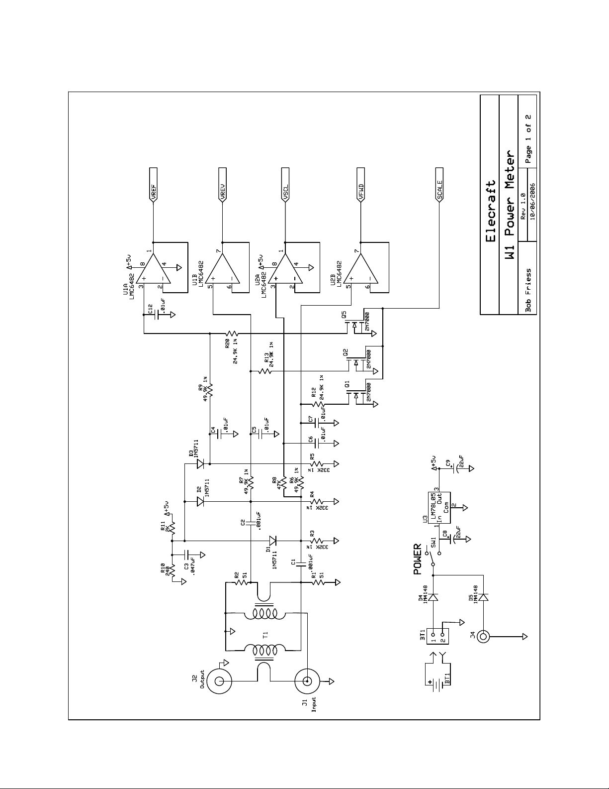
Schematic Diagram, Sheet 1
12
Page 13
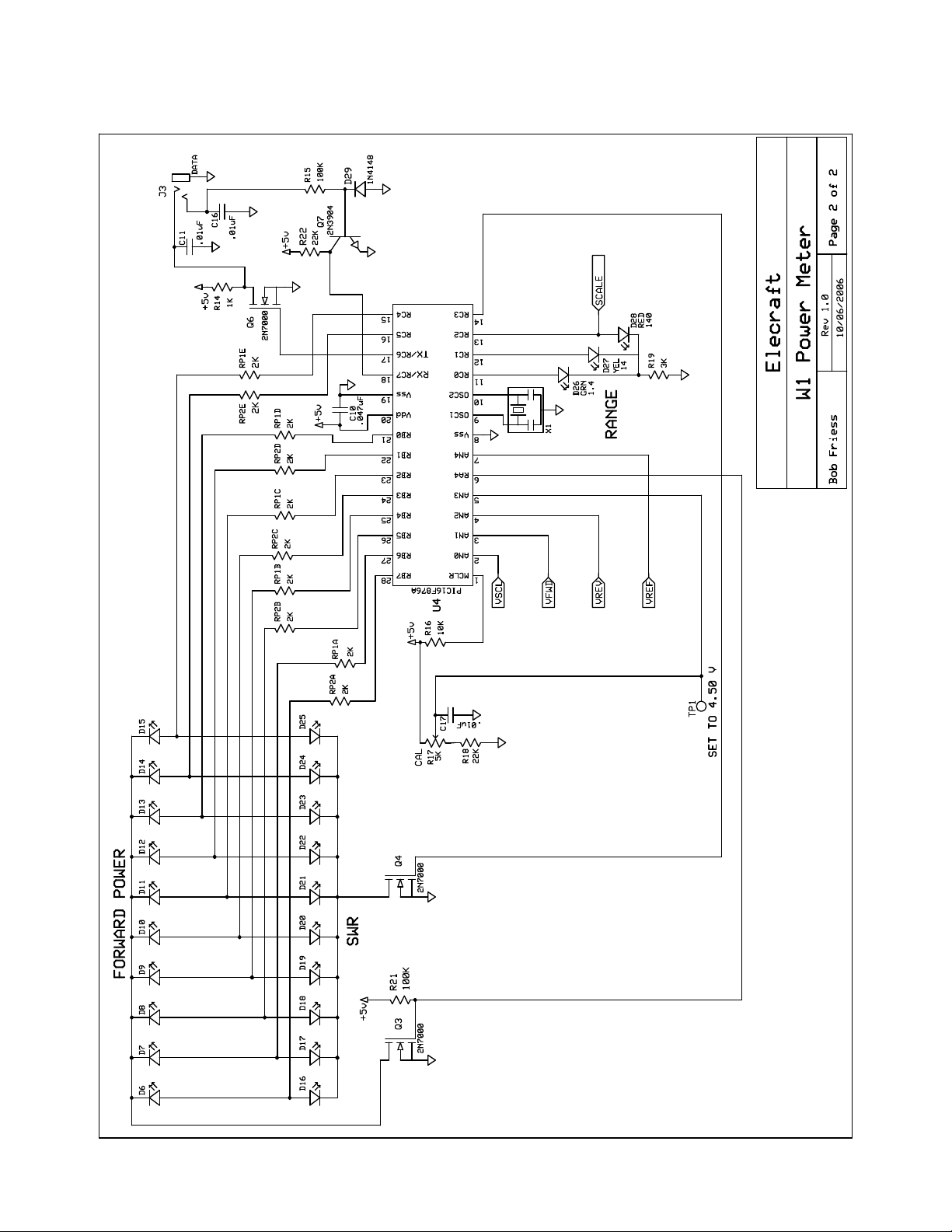
Schematic Diagram, Sheet 2
13
Page 14

Serial Interface Commands
The W1 responds to commands for data supplied by the external system. Nothing is sent until a command is received by the
W1. These requests are in the form of a single letter as shown below. The user sends a single character and receives one data
string in response. The semicolon (;) is an end-of-string identifier, and will be at the end of every return string. All strings are
fixed length; a space may be added to some strings to ensure this.
Command
Purpose
String Length
B
Response
Notes
Purpose
String Length
C
Response
Notes
Purpose
String Length
D
Response
Notes
Purpose
String Length
Response
F
Notes
Purpose
String Length
L
Response
Notes
Purpose
String Length
M
Response
Notes
Purpose
String Length 5 chars.
N
Response M<AVG|PEP>;
Notes Current setting can be saved in memory.
Request forward-power bargraph level and
present range.
5 chars.
B<L|M|H>nn;
<L|M|H> is the Range (Low|Medium|High)
nn is 00 (no LEDs lit) to 10 (all LEDs lit).
Request reverse-power bargraph level and
present range.
5 chars.
C<L|M|H>nn;
<L|M|H> is the Range (Low|Medium|High)
nn is 00 (no LEDs lit) to 10 (all LEDs lit).
Request SWR bargraph level.
4 chars.
Dnn;
nn is 00 (no LEDs lit) to 10 (all LEDs lit).
Request Forward Power in Watts.
6 chars.
F<n.nn|nn.n|nnn >;
Response is floating point.
n.nn is power from 0.000 to 9.99 watts nn.n
is power from 10.00 to 99.9 watts
nnn is power from 100.0 to 149 watts.
Toggles W1 LEDs on or off.
5 chars.
L<OFF|ON >;
Power On default is On.
Toggles between an Average or PEP
display of Forward Power LEDs.
5 chars.
M<AVG|PEP>;
Current setting can be saved in memory.
Toggles between an Average or PEP value
of Power serial data.
14
Command
Purpose
String Length 5 chars.
P
Response PK<NO|ON>;
Notes
Purpose Request Reverse Power in Watts.
String Length 6 chars.
Response R<n.nn|nn.n|nnn >;
R
Notes
Purpose Request the SWR value.
String Length
S
Response
Notes
Purpose
String Length 6 chars.
Response U<A|P><A|P><S|M|F><S|M|F>;
U
Notes
Purpose Request the firmware version.
String Length 6 chars.
V
Response Vn.nn;
Notes n.nn is the version of 1.00 to 9.99.
Purpose
W
String Length 4 chars.
Response WOk; ("Write attempt OK").
Notes
Toggles between regular LED bargraph or
Peak-Hold + bargraph.
Peak-hold default is No. Current setting
can be saved in memory.
Response is floating point.
n.nn is power from 0.000 to 9.99 watts
nn.n is power from 10.00 to 99.9 watts
nnn is power from 100.0 to 149 watts.
6 chars.
Snn.n;
nn.n is the SWR from 1.0 to 99.9.
Request the user settings that were last
stored in EEPROM
First A or P is Average power or PEP for
Forward Power LEDs. Second A or P is
Average power or PEP for Forward or
Reverse Power serial data. First S or M or
F is Slow or Medium or Fast LED decay
Rate. Second S or M or F is Slow or
Medium of Fast Range drop rate.
Writes to EEPROM the user settings
currently being used in RAM
Page 15

Command
Purpose
String Length 6 chars.
Response X<A|P><A|P><S|M|F><S|M|F>;
X
Notes
Purpose
String Length 3 chars.
0
Response A0;
This is the power on default.
Notes
Purpose Set W1 Range to Low.
String Length 3 chars.
1
Response A1;
Notes
Purpose
String Length 3 chars
2
Response A2;
Notes
Purpose Set W1 Range to High.
String Length 3 chars.
3
Response A3;
Notes
Purpose
String Length 3 chars
4
Response HS;
Current setting can be saved in memory.
Notes
Purpose Set LED decay rate to Medium.
String Length 3 chars.
5
Response HM;
Notes Current setting can be saved in memory.
Purpose Set LED decay rate to Fast.
String Length 3 chars
6
Response HF;
Current setting can be saved in memory.
Notes
Purpose Set Range drop rate to Slow.
String Length 3 chars.
7
Response YS;
Notes Current setting can be saved in memory.
Purpose Set Range drop rate to Medium.
String Length 3 chars.
8
Response Current setting can be saved in memory.
Notes
Purpose Set Range drop rate to Fast.
String Length 3 chars.
9
Response Current setting can be saved in memory.
Notes
Request the user settings currently being
used in RAM
First A or P is Average power or PEP for
Forward Power LEDs. Second A or P is
Average power or PEP for Forward or
Reverse Power serial data. First S or M
or F is Slow or Medium or Fast LED
decay Rate Second S or M or F
is Slow or Medium of Fast Range drop
rate.
Set W1 to Autorange.
Set W1 Range to Medium.
Set LED decay rate to Slow.
15
 Loading...