

Page 1

ELECRAFT T1 AUTOMATIC ANTENNA TUNER
Assembly Manual
Revision D1, October 18, 2011. Copyright © 2011, Elecraft; All Rights Reserved
Introduction
This manual covers assembly of the Elecraft T1 automatic antenna tuner. Operating instructions,
troubleshooting procedures, schematic diagram and customer service information can be found in your T1
Owner’s Manual.
Tools Required
You will need the following tools to build this kit:
Fine-tip temperature-controlled ESD-safe soldering station with 700 to 800F tip (370-430C).
Recommend a spade tip no greater than 0.05” (1.3 mm) wide.
High wattage (approx. 100 watt ) solde r ing gun to solder the BNC connectors. Use this iron only
where directed in the procedure. Use the temperature-controlled station for all other soldering.
IC-grade, small-diameter (.031”) solder (Kester #44 or equivalent). Small diameter solder is
important to avoid filling adjacent solder pads and creating solder bridg e s.
i
DO NOT use acid-core solder, water-soluble flux solder, additional flux or solvents
of any kind. Use of any of these will void your warranty.
Small, #2 Phillips screwdriver.
Needle-nose pliers.
Small wrench or driver for 6-32 nut.
Small-point diagonal cutters. Fl ush -cutting type required (Xcelite MS54-5J or equivalent).
Digital Multimeter (DMM) with voltage, resistance and diode-checking functions. A DMM with
capacitance measurement capability is desirable, but not required.
Magnifying visor or magnifying glass with a hands-free stand.
Desoldering tools and supplies are invaluable. Narrow solder wick or a good vacuum desoldering
tool such as the Soldapullt® model DS017LS are recommended.
Small, #2 (1.4 mm wide) blade screwdriver may be required.
Elecraft • www.elecraft.com • 831-763-4211
Page 2

We strongly recommend that you use a conductive wrist strap and anti-static mat while handling the MCU
or the PC boards with the MCU installed. Wrist straps and mats are available at very low cost from Jameco,
Mouser, and other electronics suppliers.
Refer to www.elecraft.com for tool sources and solder recommendations.
Unpacking and Inventory
Preventing Electro-Static Discharge Damage
The Master Control Unit (MCU) used in the T1 automatic antenna tuner is sensitive to Electro-Static
Discharge (ESD) damage. ESD damage may not make the tuner fail completely. Sometimes the unit may
continue to operate somewhat, creating a very difficult-to-find problem. We strongly recommend that you
take the following precautions whenever handling the MCU or the PC boards when the MCU is installed.
The precautions are listed in their order of importa nce:
1. Leave the MCU in its anti-static packaging until you install it.
2. Wear a conductive wrist strap with a 1-megohm series resistor when handling the MCU or the
boards with the MCU installed. If you do not have a wrist strap, frequently touch an unpainted
ground while working. You can collect a destructive charge on your body just sitting at the work
bench. Do not attach a ground directly to yourself as this poses a serious shock hazard.
3. Use an ESD-safe soldering iron with a grounded tip.
4. Use a grounded anti-static mat on your work bench.
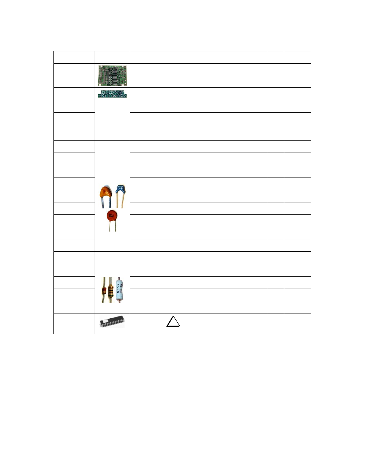
Identifying Capacitors
Capacitors are identified by their value and the spacing of their leads.
Small-value fixed capacitors are usually marked wit h o ne, two, or t hree di gi t s and n o dec imal point. If one
or two digits are used, that is the value in picofarads (pF). If there are three digits, the third digit is a
multiplier. For example, a capacitor marked "151" would be 150 pF (15 with a multiplier of 10
"330" would be 33 pF, and "102" would be 1000 pF (or .001 µF). Exceptions are described specifically in
the text and parts list.
Fixed capacitors with values of 1000 pF or higher often use a decimal point in the value, such as .001, .047,
or 2.2. This is the value in microfarads (µF) (1 µF is equal to 1,000,000 pF).
Most of the capacitors in this kit have a lead spacing of 0.2”. When a capacitor with a lead spacing of 0.1”
is called for, it is stated in the description, e.g. Capacitor C20, .01 µF, LS 0.1” (103).
Identifying Resistors
Resistors are identified by their power dissipation rating and their resistance value. The power rating is
indicated by their physical size. There are both 1/4 watt and 1/8 watt resistors in your T1 tuner kit. The 1/8
watt resistors are about one-half the size of the 1/4 watt resistors.
2
1
). Similarly,
Page 3
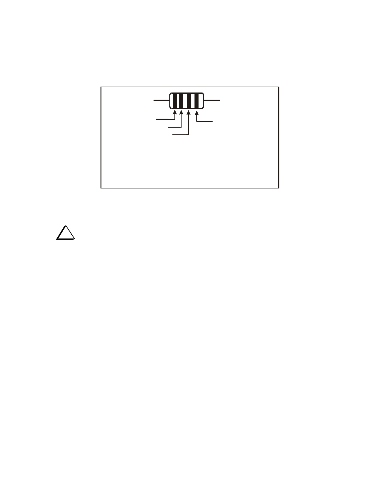
The color bands that indicate the value of resistors are shown in the text to help you identify the correct
part. However, it’s helpful to familiarize yourself with the color code (see Figure 1). For example, a resistor
with the color bands of brown, red, yellow, gold would be a 120K ohm, 5% resistor. This resistor will be
identified in the text as 120K ohm (brn-red-yel).
If you are in doubt about a resistor’s value, use a DMM. Do not be concerned with minor deviations from
the expected value. Typical errors on most DMMs and the tolerances of the resistors normally produce
readings that are slightly different from the values indicated by the color bands.
FIRST DIGIT
SECOND DIGIT
COLOR DIGIT
Black
Brown
Red
Orange
Yellow
Green
0
1
2
3
4
5
MULTIPLIER
MULTIPLIER
X 1
X 10
X 100
X 10K
X 10K
X 100K
TOLERANCE:
GOLD = 5%
SILVER = 10%
COLOR DIGIT
Blue
Violet
Gray
White
Silver
Gold
6
7
8
9
-
-
MULTIPLIER
X 1M
-
-
X 0.01
X 0.1
Figure 1. Resistor Color Code.
Soldering and Desoldering
i
Use adequate ventilation when soldering; avoid inhaling smoke or fumes. Always wash your
hands after handling solder, as lead residue is highly toxic.
When applying solder, use the minimum amount required to surround the component lead and make good
contact with its printed-circuit pad. You don't need a "fillet" (build-up ) of solder. This will avoid unwanted
solder bridges and any need to clean the PC boards.
The solder must flow onto both the component lead and its PC board pad. To ensure that both will be
heated at the same time, the tip of the iron should contact both the component lead and the PC board pad
before solder is applied.
Solder joints should be clean and shiny. If a joint appears dull or has fine cracks, it is probably cold. Cold
solder joints should be cleaned and re-soldered. First, use solder wick (desoldering braid) to remove the old
solder. Then apply fresh solder. If you have many cold solder joints, it probably indicates that your
soldering iron temperature is too low, or that the tip or solder itself is defective.
3
Page 4

Elecraft kits use high-quality double-sided PC boards. Removing components can be difficult, since you
must get all of the solder back out of the hole before a lead can be removed. To do this, you'll need solder
wick (desoldering braid) and/or a vacuum desoldering tool. It also takes some practice. A number of
suggestions are provided below.
The best strategy for avoiding de-soldering is to place all components properly the first time. Double-check
values and orientations, and avoid damaging parts via ESD.
When removing components:
Don't pull a lead or pin out of a hole unless the solder has been removed or you are applying heat.
Otherwise you can literally pull the plating out of the plated-through hole.
Limit soldering iron contact to a few seconds at a time.
Use small-size solder-wick, about 0.1" or 2.5 mm wide. Use the wick on both the top and bottom pads
when possible. This helps get all of the solder out of the hole.
If you use a vacuum desoldering tool (solder sucker), use a large unit. Small solder suckers are not
very effective.
The safest way to remove ICs and other components with more than 3 leads is to clip all of the pins at
the body of the device first, then remove all of the pins individually. You may damage pads and traces
by trying to remove such components intact.
Invest in a PC board vice with a heavy base if possible. This makes parts removal easier because it
frees up both hands.
If in doubt about a particular repair, ask for advice from Elecraft or from someone else with PCB repair
experience.
4
Page 5
Parts List
We strongly recommend that you do a complete inventory before beginning assembly. The inventory helps
you correctly identify all the parts to avoid mistakes during assembly.
Ref. Photo Description Qty
T1 main PC board (larger board). This board has a number of
Misc.
Misc.
C8,9,11,12,
C15, 16, 17, 18,
CA, CB, CC,
CD, CE, CF,
CG, CH, CJ,
CK, CL, CM,
CN, CP, CR
C1, C5A
C10 Capacitor .001 µF, LS 0.1" (102) 1 E530074
C19 Capacitor 1.0 µF non-polarized, LS 0.1" (105) 1 E530174
C2 Capacitor, 20 pF, 500 V, NPO or C0G (20) 1 E530173
C3 Capacitor 39 pF, 500 V (39) 1 E530028
C4 Capacitor 82 pF, 500 V (82) 1 E530095
C5 Capacitor 150 pF, 500 V (151) 1 E530097
C6, C7, C7A Capacitor 330 pF, 500 V (331) 3 E530409
Pre-Installed
Surface-
Mount
Devices
Typical
Capacitor
Styles
surface-mount device (SMD) capacitors pre-installed on the
bottom.
T1 control PC board 1 E100236
Capacitor .01 µF 8 E530175
Capacitor .01 µF. On the PC board, these capacitors are
identified only by the second letter (e.g. A, B, C, D...)
Capacitor 10 pF, 500 V (10) 2 E530026
1 E850198
15 E530175
Part
Number
C20 Capacitor .01 µF, LS 0.1" (103) 1 E530019
R1,R2
R11 Resistor, 24K, 1/8 W, 5% (red-yel-org) 1 E500155
R3,R4,R13,
R14,R21
R5, R6, R7,
R10
R9 Resistor, 180 ohms, 1/8 W, 5% (brn-gry-brn) 1 E500157
U1
Resistors
1/8 -1/4 -1W
Resistor, 51 ohms, 1 W, 5% (grn-brn-blk or stamped 510J) 2 E500159
Resistor, 3.3K, 1/8 W, 5% (org-org-red) 5 E500156
Resistor, 120K, 1/8 W, 5% (brn-red-yel) 4 E500154
MCU,16F876A
i
ESD Sensitive! Do not remove from
its packaging until instructed to do so.
1 E610020
5
Page 6
Ref. Photo Description Qty
Q1
Transistor 2N3906 1 E580000
Part
Number
U2 I.C. L78L06 or LM78L06 1 E600001
D1,D2, D4
D3
J1,J2
J3
J4, J5
P1, P2
Misc.
D6
D7 LED, yellow 1 E570020
D8 LED, red 1 E570019
Misc.
Z1
S1,S2
K1-K15
T1,T2
Diode 1N5711 3 E560004
Diode 1N5817 1 E560008
BNC female, PCB mount 2 E620075
Stereo jack, 3.5 mm, miniature 1 E620087
Conn., 0.1" spacing, 6 pin female, low-profile 2 E620096
Conn., 0.1" spacing, 6 pin male 2 E620095
Socket for U1, low-profile, 28 pins 1 E620074
LED, green 1 E570021
LED spacer 3 E570024
Ceramic resonator, 4.0 MHz 1 E660001
Switch, Tactile, SPST, 6 mm, actuator length 7 mm 2 E640022
Miniature DPDT relay 15 E640010
Toroid, FT37-43 (Gray) 3 E680003
L1-L5 Toroid, T37-6 (Yellow) 5 E680013
L6-L7 Toroid, T37-2 (Red) 2 E680006
Hardware
Hardware
Hardware
Hardware
Hardware
Hex nut, 6-32 1 E700040
Flat washer, #6 1 E700067
Knurled thumb-nut, brass, 6-32 1 E700094
Lock washer, #6 internal tooth, stainless 1 E700095
Solder lug, #6 1 E700096
6
Page 7
Ref. Photo Description Qty
Hardware
Hardware
Screw, 6-32 x 9/16” 1 E700100
Screw, #2, 9/16 inch self tapping 4 E700097
Part
Number
Misc.
Misc.
Misc. Enamel wire, #26, red 10 ft. E760002
Misc. Hookup wire, 28 AWG stranded, black 6 in. E760026
Misc. Hookup wire, 28 AWG stranded, red 6 in. E760027
Misc. Hookup wire, #24 solid, green insulation 6 in. E760008
Misc. T1 front panel label 1 E980104
Misc. T1 cover spacer, 1x1.75x0.125", foam, black, self-adhesive 1 E980107
Misc. T1 enclosure top and bottom cover 1 E100204
Misc. T1 enclosure end cover 1 E980106
Misc. T1 owner's manual 1 E740079
Misc. T1 assembly manual 1 E740080
9-volt battery clip, wide 1 E700099
9-volt battery clip, narrow 1 E700098
7
Page 8
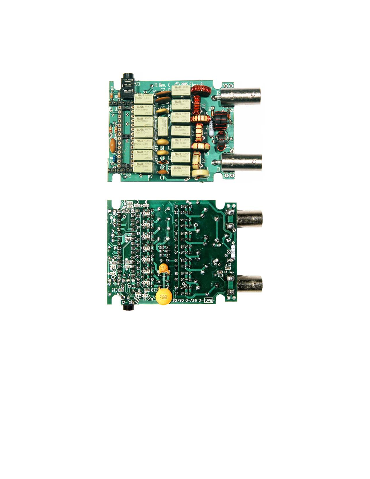
Main PC Board Assembly
The main PC board is the larger of the two boards. The completed PC board is shown in Figure 2. Use this
figure for reference, but follow the step-by-step procedures as given. Some parts are very difficult to install
if done in the wrong sequence. Many parts are almost impossi bl e to remove without destroying the part or
damaging the PC board.
Top
Bottom
Figure 2. Completed Main PC Board.
8
Page 9
Main PC Board Assembly Procedure – Part I
OU
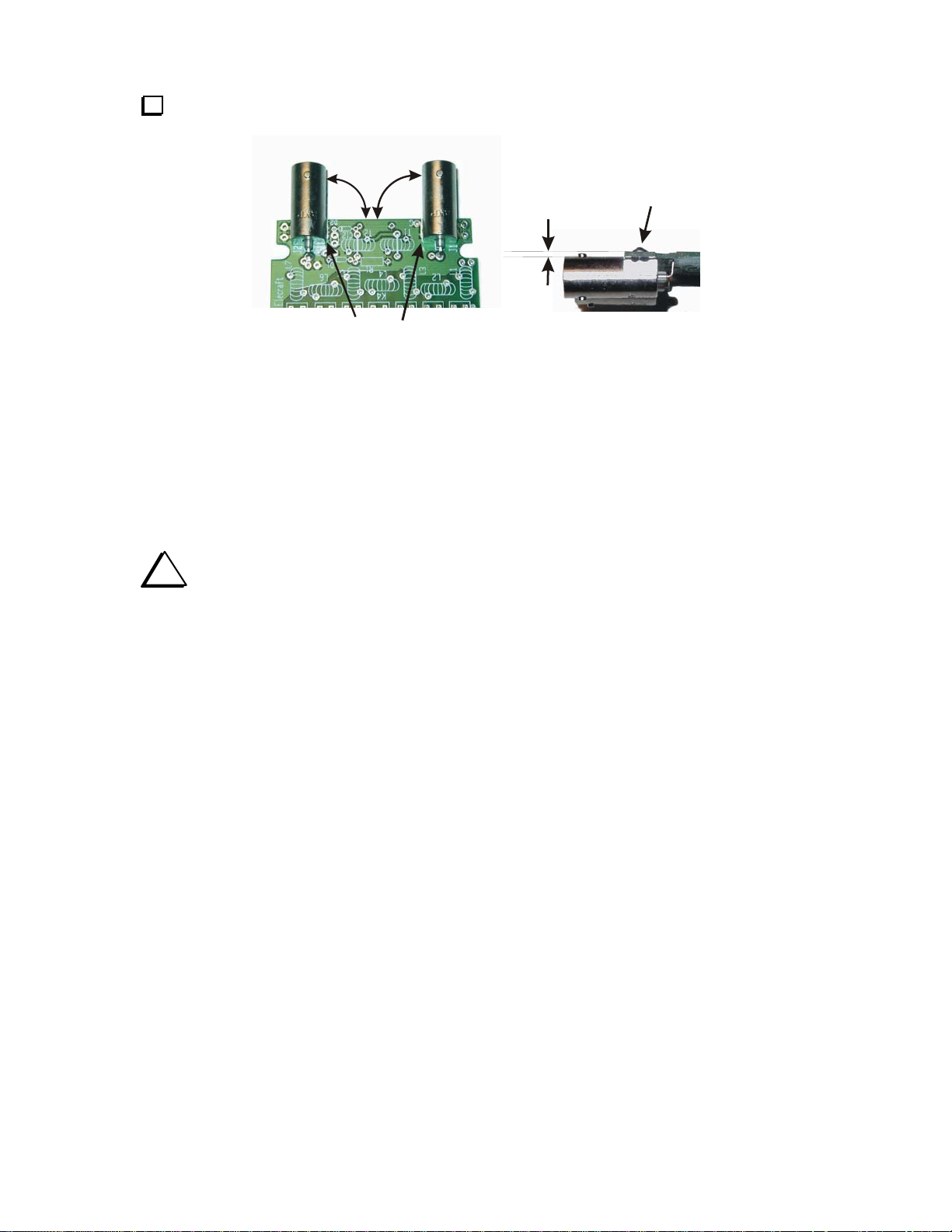
S
Install BNC connectors J1 and J2 as follows. When completed they must be aligned as shown
in Figure 3.
O
90
JACKS CENTERED
WITHIN
PRINTED
TLINE
JACK BARRELS
PARALLEL WITH
BOARD
USE HEAVY-DUTY
IRON TO SOLDER
MOUNTING NUBS
(SEE TEXT)
Figure 3. Installing J1 and J2.
__ Position BNC connector J1 on the board over the printed outline as shown with the mounting nubs and
center connector passing through the holes provided. Be certain the barrel is at a 90-degree angle with the
edge of the board and parallel to the board as shown in Figure 3.
__ While holding the connector in place, wet the tip of your iron with a drop of solder and use it to
temporarily tack-solder the connector center terminal.
__ Check to ensure the connector is still aligned as shown in Figure 3. If not, re-heat the tack soldered join t
and adjust the position. It will be very difficult to adjust the connector after you complete the next step.
i
In the following step you will use a large iron to solder the two mounting nubs on the BNC
connector to the board. This is the only time you should use anything other than a temperature-
controlled, ESD-protected soldering station to assemble your T1 tuner.
__ Place the board the bottom side up on a surface that wi ll not be dam aged if body of the BNC connector
becomes warm. Apply the large iron and solder to the end of one amounting nub where it protrudes through
the circuit board. Remove the iron as soon as the solder flows onto the pad. Do not put the iron directly on
the solder pad. Do not be concerned if solder fills the pad marked G near J1.
__ Solder the second mounting nub using the same procedure.
__ Using your temperature-controlled iron, properly solder the center pin that you tack-soldered earlier.
__ Repeat the above procedure to install the second BNC connector, J2.
9
Page 10

i
A
Use only your temperature-controlled, ESD-protected soldering station for the remainder of
the assembly.
Bend the leads for R1, 51 ohms (grn-brn-blk or 510J), 1 watt, at right angles to the body. Insert the
leads in the solder pad holes at the ends of the printed outline between J1 and J2. There are three holes very
close together at the end of R1 near J2. Be sure the leads go through the proper holes in the board, indicated
by short white lines on the part outline. On the bottom side of the board, bend the leads out at 45-degree
angles to hold the resistor in place.
Check the position of the resistor to be sure it is centered in the printed outline and flush against the
board as shown in Figure 4. Solder, taking care not to get solder in either of the empty holes at the J2 end of
the resistor. Trim the leads flush with the bottom of the board.
ENSURE MARKINGS AGREE WITH
INSTRUCTIONS IN TEXT
BODY OF PART
GAINST THE BOARD
SOLDER & TRIM LEADS FLUSH
Figure 4. Installing Resistors.
i
From this point forward, instructions to “install” a component mean to position it within its
outline against the board, solder and trim the leads flush on the opposite side.
Install the following resistors in the outlines shown at the end of the PC board opposite BNC
connectors J1 and J2. These resistors are 1/8 watt resistors, about half the size of R1.
__ R5, 120K (brn-red-yel) 1/8 W
__ R3, 3.3K (org-org-red) 1/8 W
__ R6, 120K (brn-red-yel) 1/8 W
__ R4, 3.3K (org-org-red) 1/8 W
Locate capacitor C1, 10 pF (10). Note that the capacitors may have markings on their bodies in
addition to the value given in parenthesis.
Insert C1 into the holes in the outline on the PC board. With the BNC connectors toward you, the
position for C1 is about half way back on the left edge. If necessary, gently straighten the leads so the
capacitor will sit close to the board without excessive lead lengths as shown in Figure 5. When
straightening the leads, do not tug on them. Squeeze and bend the leads with your pliers to straighten them.
Chipping of the insulation around the leads will not harm the capacitor.
10
Page 11

G
SO
THE NUMBERS IN PARENTESIS
IN THE TEXT MUST APPEAR ON
THE BODY. USUALLY THERE
ARE OTHER MARKINGS AS WELL.
10
ENTLY FORM LEADS
CAPACITOR SITS AS CLOSE
TO THE BOARD AS THE
INSULATION ALLOWS.
SOLDER & TRIM LEADS.
Figure 5. Installing Capacitors.
Bend the leads out at 45-degree angles on the bottom side of the board to hold the capacitor in place,
then solder and trim the leads flush with the bottom of the board.
Install the following capacitors in the outlines shown across the center of the PC board adjacent to C1.
__ C2, 20 pF (20)
__ C3, 39 pF (39)
__ C4, 82 pF (82)
Install the following capacitors in the outlines shown across the next to the ones you just installed. Be
careful to insert the leads in the correct solder pads. There are solder pads very close to those for C5 and C7
for two capacitors that will be installed on the bottom of the PC board later. Make sure you don’t use these
pads by mistake. Also, be sure the larger capacitors are positioned so they do not overlap the outlines for
the relays on either side.
__ C5, 150 pF (151)
__ C6, 330 pF (331)
__ C7, 330 pF (331)
Install capacitor C10, .001 µF, LS 0.1” (102) in the outline at the end of the PC board farthest from
BNC connectors J1 and J2. Look closely at the marking. Do not use (105) my mistake.
Locate diode D1 (1N5711). You may need to use a strong magnifier to read the numbers. The
numbers are often printed on the body in two rows of three letters each (e.g. 1N5 and 711)
Locate the outline for D1 on the circuit board near J2 and R1. Note that the printed outline has a band
near one end.
Gently bend D1’s leads at right angles to the body and insert it into the solder pad holes with the
banded end of the diode toward the banded end on the printed outline. On the bottom of the board, bend the
leads at 45 degree angles to hold it in place.
i
Your T1 tuner will not operate correctly if the banded end of the diode is not aligned with the
banded end of the outline on the PC board.
Solder the leads and trim them flush.
Install diode D2 (1N5711) the same way you installed D1. D2 is close to BNC connector J2.
11
Page 12

Locate the 15 relays and carefully remove them from the carrying tube(s). Check the relays for bent
pins. Carefully straighten any bent pins using needle-nose pliers.
Locate a small book or other smooth, flat object somewhat larger than the PC board that is easy to
handle. You will use this to hold the relays in place on the PC board before soldering them.
Hold the PC board in one hand and drop the relays into the spaces shown for K1 through K15. Note
that the pin spacing only allows them to go in when oriented properly. Do not use force. They should
simply drop into place. Don’t miss K12 that sits between the two long rows of relays.
Place the book against the top of the relays and then, holding the book and PC board together to keep
the relays from falling out, flip the whole assembly over and set it down.
i
Relays K9 through K15 have small SMD capacitors between their pins. Take care soldering.
Do not create solder bridges between the relay pads and the SMD pads.
On each of the 15 relays, tack-solder only one corner pin to hold it in place.
i
Do not touch the plastic relay covers with your soldering iron. Even a small burn or melted
spot may jam the relay mechanism inside.
Re-heat the soldered pin on each relay while pressing down on it to ensure that it is squarely against
the PC board. The relays should be aligned in neat rows with the tops level.
When you are satisfied with the position of the relays, solder the remaining pins.
i
Do not trim or bend the relay pins after soldering. Trimming or bending the pins introduces
mechanical stresses that may cause premature relay failure.
Check all fifteen relays carefully to ensure that every pin is soldered and that there are no solder
bridges between pins.
12
Page 13

Inspect the 28-pin, low-profile socket for U1. Note that:
C
__ Each pin has a shoulder. When installed, all of the shoulders must be in contact with the PC board. You
will not be able to assemble your finished tuner if this socket is not mounted against the PC board.
__ The pins are hollow. The pins on controller U1 fit inside the pins on the socket. Do not cut, bend or alter
the pins in any way or you may not be able to install U1.
__ There is a notch at one end of the black plastic frame of the socket. This notch must be aligned with the
marks on the PC board when you install the socket.
Align the socket with the outline for U1 on the top side of the PC board near the opposite end of the
board from J1 and J2. Make sure that each pin is in its corresponding solder pad, and the solder pads
reserved for P1 and P2 are open (See Figure 6). Verify that the notched end of the socket is pointing toward
the holes for connector P1 as indicated by the outline printed on the board.
ERTAIN PADS FOR P1 AND P2 ARE CLEAR
BE
NOTCHED END
OF SOCKET
Figure 6. Installing Socket for U1.
Gently press the socket down onto the board until the shoulder of each pin is touching the top of the
board. Do not solder yet. You will be instructed to do so in a later step.
Once soldered, the socket for U1 will be impossible to remove from the board without destroying it.
Before soldering, check to be certain it is positioned correctly as follows:
__ Locate the two 6-pin male connectors, P1 and P2.
__ Place the short pins of the connectors in spaces provided for P1 and P2. Figure 2 shows these
connectors in place on the finished PCB. Confirm that the socket for U1 is properly positioned so that
connectors P1 and P2 can be installed later.
__ Remove the 6-pin male connectors from P1 and P2 and set them aside. Don’t disturb the 28-pin socket.
On the 28-pin socket, solder one pin, then inspect the socket carefully to ensure that the shoulders of
the pins are against the top of the board. If needed, reheat the pi n w hil e pr essi ng the down on the socket.
When you are satisfied that the socket is seated against the top of the board, solder all 28 pins.
13
Page 14

On the top of the board, position ceramic resonator Z1 (4.00 MG) in the outline between the socket for
5
U1 and the edge of the board. Even though it may have a red dot on one end, the resonator may be installed
in either direction. Hold the resonator so the insulation on the leads is against the top of the board, then
tack-solder one pin. Verify that the insulation of all three leads is against the top of the board. If it is
allowed to sit too high it will strike the control board when you assemble the tuner.
Solder all three pins on Z1.
Position the miniature stereo jack in the outline for J3 on the top of the board. The round portion of the
jack will extend over the edge of the board. Hold the jack against the board and tack-solder one pin. Verify
that the jack is solidly against the board, otherwise it may not line up with the hole in the enclosure when
you assemble your tuner.
i
Use no more solder than is necessary for a good joint on J3. Filling the holes with too much
solder may allow it to flow into the jack and ruin it.
Solder all three pins on J3.
Locate the two 6-pin male connectors, P1 and P2, that you just test-fitted on the board, and the two
6-pin female connectors J4 and J5.
Insert the longer pins of the male connectors into the female connectors. Be sure the connectors are
fully mated. There may be a small gap remaining between the plastic parts.
Refer to Figure 7. Place the pins of P1 and P2 into position at each end of the 28-pin socket on the
main PC board, then place the control PC board on the pins of J4 and J5 as shown. Be sure the control
board is oriented with the top side shown in the figure facing up. The ends of the control board should line
up with the sides of the main PC board. The notched corners must be over the cutouts near the corners of
the main PC board.
RELAYS ON MAIN PCB
THIS SIDE MUST FACE UP
J4
P1
J4
SHORT PINS
J5
P2
Figure 7. Installing P1, J4, P2 and J5.
Hold the assembly and tack-solder one terminal on P1, P2, J4 and J5. Do not to touch the relays with
your soldering iron.
14
J
Page 15

Inspect the assembly to be certain the control PC board is oriented as shown in the figure. The top of
the board should be level with and slightly below the top of the relays next to it. The connectors must be
square against the two boards. If necessary, reheat the soldered pins and adjust the connectors. The
assembly must be as shown for the tuner to fit in its enclosure properly.
Solder all the pins on P1, P2 J4 and J5. At P1, be careful not to create a solder bridge between
pin 3 and the solder pad for resistor R4 that is very close.
Unplug the control PC board and set it aside.
On the bottom side of the board between BNC connectors J1 and J2, install resistor R2, 51 ohms
(grn-brn-blk or 510J), 1 watt. Trim the leads flush with the top of the board.
Install C7A on the bottom of the board as follows:
__ On the bottom side of the board, locate the outline for capacitor C7A.
__ Insert the leads for C7A, 330 pF (331) through the solder pads and fold the capacitor down flat against
the board toward the edge. Orient it so you can read the value. Do not solder yet!
__ Remove C7A and pre-trim its leads so they pass through the solder pads but do not protrude through the
top side of the board. If necessary, remove a small amount of the insulation from around the leads near the
capacitor body to expose the lead and solder pad.
__ Solder C7A in place from the bottom of the board.
Install C5A, 10 pF (10) on the bottom of the board in the same way you installed C7A. Fold C5A
toward the pins of K14 at the center of the board.
Resistance Checks
Make the following resistance checks between the various pins of socket U1. Pin 1 is nearest the edge
of the board at the end near the stereo jack. Count down the row, across the end and back up the other side.
Pin 28 is across from pin 1 at the end near the stereo jack.
√
U1 Pins Resistance
√
U1 Pins Resistance
4 – 11 400 – 420 ohms 4 – 23 400 – 420 ohms
4 – 12 400 – 420 ohms 4 – 24 400 – 420 ohms
4 – 13 400 – 420 ohms 4 – 25 400 – 420 ohms
4 – 14 400 – 420 ohms 4 – 26 400 – 420 ohms
4 – 15 400 – 420 ohms 4 – 27 400 – 420 ohms
4 – 16 400 – 420 ohms 4 – 28 400 – 420 ohms
4 – 21 400 – 420 ohms 20 – 8 > 100 k or Inf.
4 – 22 400 – 420 ohms 10 – 8 > 100 k or Inf.
15
Page 16

Main PC Board Assembly Procedure – Part II
i
In the following steps you’ll wind and install the toroidal transformers and inductors. They
must be wound on the correct toroid core exactly as described or your tuner will not operate
properly.
1
Wind transformer T1 as follows:
__ Locate an FT37-43 toroid core. This is a dark grey core that is not painted. There are three of them in
the kit.
__ Cut a 7-inch (18 cm) length of the red enameled wire.
__ “Sew” the long end of the wire through the hole in the core for a total of 8 turns. Count one turn each
time the wire passes through the center of the core. There are no half or quarter turns when winding a
toroid. Match the winding direction shown in Figure 8 so the leads will line up with the solder pads on
the circuit board.
__ Spread the turns around the core as shown in the figure.
GREEN
T1 READY FOR
INSTALLATION
PRIMARY
SMALLER
SECONDARY
LEAD
LEAD
LEAD POSITIONS
ON PC BOARD
SMALLER
SECONDARY
LEAD
GREEN
PRIMARY
LEAD
T1 INSTALLATION
COMPLETE
Figure 8. Transformer T1.
Strip the insulation and tin the leads using one of the following methods. Strip off the enamel all the
way up to the core. It will not hurt performance if the tinned area of the lead touches the core.
1. Heat stripping: Melt a blob of solder on the tip of your iron and insert the clipped end of the lead
in the blob. The insulation will bubble and vaporize after about 5 seconds. Add solder and feed the
wire into the blob up to the edge of the core, then slowly pull the wire out of the solder. If any
enamel remains on the lead, scrape it away.
2. Burn the insulation off by heating it with a butane lighter for a few seconds. Remove any residue
with sandpaper, then tin the bare wire.
3. Scrape the wire with a sharp tool. Take care not to nick the wire. Remove all the insulation around
the entire circumference of the wire, then tin the wire.
1
Prewound toroids are available from an Elecraft-approved source. See www.elecraft.com for details.
16
Page 17

i
The leads must be stripped of insulation and tinned correctly to provide good electrical
contact when installed. Carefully inspect each tinned lead for:
A clean, tinned lead with no enamel residue left under the tinning.
The lead must be tinned all the way around the wire.
The lead should be tinned all the way up to the core as shown in Figure 8.
Locate the outline for T1 between BNC connectors J1 and J2 on the PC board. Thread the tinned leads
of T1 through the smaller pads (See Figure 8). Position the toroid over the outline as shown and bend the
leads on the bottom of the circuit board to hold the toroid against the PC board in place. Inspect the lead on
the top side of the board to be sure tinned lead is visible above the solder pad. If not, remove the toroid,
clean and tin the lead closer to the core and replace it on the PC board.
Solder and trim both leads flush, then adjust the position of T1, if needed, so it sits within the outline
printed on the PC board.
Cut a 3/4” (19 mm) length of the green insulated solid wire. Strip the insulation from 1/4” (6 mm) at
each end of the wire.
Thread the wire through the center of T1 and into the holes on either side of the printed outline for T1
on the PC board to form the 1-turn primary winding for the transformer. Solder and trim the wires flush
with the bottom of the board.
Transformer T2 is identical to T1 except that it uses two FT37-43 cores stacked together as shown in
Figure 9. To simplify winding the secondary, you may wish to glue the core s together using epoxy or
cyanoacrylate adhesive (super glue). Prepare and install transformer T2 using:
_ 15” (39 cm) of red enamel wire for the secondary and wind 8 turns (wire passes through the
center 8 times).
_ 1” (25.4 mm) of green insulated wire for the primary winding. Strip 1/8” (3mm) from each end.
Because of the tight fit, you may find it easier to prepare the green primary wire, loop it through the toroid,
then insert the secondary leads and the green primary leads into the pc board pads at the same time.
GREEN
PRIMARY
SMALLER
SECONDARY
LEAD
LEAD
SMALLER
SECONDARY
LEAD
GREEN
PRIMARY
LEAD
T2 SECONDARY WOUND
ON TWO FT37-43 CORES
BE CERTAIN THE LEADS ARE INSTALLED
IN THE CORRECT PC BOARD PADS
Figure 9. Transformer T2.
17
T2 INSTALLATION
COMPLETE
Page 18

Locate the five T37-6 yellow toroids. Use these toroids to prepare inductors L1 through L5 as listed
S
S
S
S
below. Position the turns on each toroid as shown in Figure 10 so the leads will line up with the holes in the
PC board. Note that L1 is wound in the opposite direction from the others. Install each coil with the core
upright against the top of the board inside its printed outline. Solder and trim the leads.
Inductor Wire Length Number of Turns Core
L1 6” (16 cm) 3 close wound Yellow
L2 6.5” (17 cm) 5 spaced Yellow
L3 7” (18 cm) 7 spaced Yellow
L4 9” (23 cm) 11 spaced Yellow
L5 11” (28 cm) 16 spaced Yellow
L1 - 3 TURNS L2 - 5 TURNS
L3 - 7 TURNS
L4 - 11 TURN
L5 - 16 TURN
Figure 10. Toroid Inductors L1 - L5.
i
Do not use glue or other fixative to hold the toroids on the PC board. Such materials may
affect their electrical characteristics. The toroids need no support other than their own leads.
Locate the two T37-2 red toroids. Use these toroids to prepare L6 and L7 and install them in the
remaining spaces shown on the PC board.
Inductor Wire Length Number of Turns Core
L6 13” (33 cm) 20 spaced Red
L7 18” (46 cm) 29 close wound Red
L6 - 20 TURN
L7 - 29 TURN
Figure 11. Toroid Inductors L6 and L7.
18
Page 19

Visual Inspection
Use a magnifier and good light to check the board for the following:
Missed solder connections. Look closely at each relay pin.
Solder bridges. Look closely at the SMD capacitors between the relay pins.
Properly tinned toroid leads. You should see some tinned lead above the PC board on every toroid. Be
suspicious of any leads where the enameled part of the wire goes into the solder pad. If in doubt, remove,
clean and tin more of the lead or rewind the toroid.
Diode orientation. The banded ends of D1 and D2 must be nearest BNC connector J2.
Control Board Assembly
The completed control PC board is shown in Figure 12. All of the components are mounted on the top of
the board. There is very little excess space above or below this board when your tuner is assembled in its
enclosure. Follow the instructions carefully to ensure the board will fit when you assemble your tuner.
i
It is almost impossible to remove a part without destroying the part or damaging the board.
Double-check the position and value of all parts installed on the control board before soldering.
Figure 12. Completed Control PC Board.
19
Page 20

Control Board Assembly Procedure
D
Install resistor R10, 120K (brn-red-yel), 1/8 watt.
i
When your tuner is assembled, the bottom of the control PC board will be very close to the
top of the MCU. It is critical to flush cut all leads on the bottom of the board in the area directly over
the MCU to no more than 1/32” (1 mm) in height.
Locate voltage regulator U2 (78L06). This is a three-terminal device that looks like most transistors
with one flat face and a rounded back. The number is printed on the flat face, but you may have to use a
magnifier and hold it in just the right position under a strong light to see the lettering.
Install U2 as follows:
__ Bend the three leads toward the rounded side of the case, then position it on the board with the three
leads through the solder pads and the rounded side against the board (See Figure 13).
LAY AGAINST BOAR
FLAT SIDE UP.
Figure 13. Installing U2 on the Control Board.
__ On the bottom of the board, bend the leads to hold U2 in place.
__ Solder and flush-cut the center lead.
__ Adjust U2, if needed, to center it within the outline with the rounded back touching the board.
__ Solder and flush-cut the remaining two leads.
Install Q1 (2N3906) using the same procedure as you used for U2. When soldering, be careful not to
fill the open solder pad for C20.
Install diode D4 (1N5711). Orient the band over the end indicated on the circuit board.
Install C19, 1 µF, L.S 0.1 (105). Lay the capacitor body in the square shown on the control board with
the leads inserted through the solder pads. Adjust the leads to allow the body to lie as flat as possible.
Insert the leads of resistor R7, 120K (brn-red-yel), 1/8 watt, through the solder pads and bend them to
hold it in place, but do not solder yet to avoid filling the solder pad for R14.
Install resistor R14, 3.3k (org-org-re d ), 1/ 8 wat t . Sol der and flush-cut the leads for both R7 and R1 4.
Take care not to touch connector J4 with your iron while soldering.
20
Page 21

Install the following 1/8 watt resistors.
__ R9, 180 ohm (brn-gry-brn) __ R21, 3.3k (org-org-red) __ R11, 24k (red-yel-org)
Position resistor R13, 3.3K (org-org-red), 1/8 watt on the board and spread its leads to hold it in place.
Do not solder yet. You will be instructed to solder the leads in a following step.
Insert one of the pushbutton switches in the position for S2. It can be oriented either way. Make
certain the ridges on the bottom of the switch housing are against the board.
Solder one terminal of S2, then inspect the switch to make sure it is still sitting directly against the
board. If necessary, reheat the soldered terminal while pressing the switch down against the board.
When you are satisfied that the switch is against the board, solder and flush-cut the remaining
terminals of S2 and the leads to resistor R13. Take care not to touch J5 with your soldering iron.
Insert the second push-button switch in the position for S1. It can be oriented either way. Solder one
pin, then inspect the switch to make sure it is still sitting directly against the board. If necessary, reheat the
soldered terminal while pressing the switch down against the board.
When you have confirmed that the switch is in position, solder and flush-cut the remaining three
terminals.
Cut a 2-1/2” (64 mm) length of the black #28 AWG stranded wire. Strip the insulation from 1/8”
(3 mm) at each end and tin the bare wires. Insert one end in the “–” solder pad near R11 on the top of the
board, then solder and flush-cut on the bottom of the board. Dress the lead over the edge of the board next
to R11.
Slip the round spacer over the leads of the red LED.
Insert the longer lead of the red LED int o the round solder pad for D8.
i
The longer lead must go into the round solder pad or the LED will not work.
Spread the leads to hold the LED in place with the spacer against the board. Solder and flush-cut the
leads.
Inspect the position of the LED to be sure it is sitting vertically against the spacer. If necessary, reheat
the solder pads one at a time while adjusting the LED position.
Following the same procedure, install the remaining two LEDs on spacers. Be sure the long leads go
into the round solder pads.
__Yellow LED at D7 __ Green LED at D6
21
Page 22

Install capacitor C20, .01 µF, LS 0.1” (103). Even though the outline does not indicate it is placed
against the board, fold it down in the direction of the red LED D8 before soldering (See Figure 12).
Bend the leads of diode D3 (1N5817) at right angles to its body and insert it in the space shown on the
control board. Be sure to orient the band over end indicated on the circuit board. Solder only the pad at the
banded end of the diode. You’ll solder the other end in the next step.
Cut a 1.5” (38 mm) length of the red #28 AWG stranded wire. Strip the insulation from 1/8” (3 mm) at
each end and tin the wires. Position one end in the “+” solder pad on the top of the control board. On the
bottom of the board, solder the wire and the remaining lead for D3, then flush-cut the excess wire and D3
lead.
Visual Inspection
Verify that there are no leads or solder fillets more that 1/32” (1 mm) high on the bottom side of the
board.
Use a magnifier and carefully check the board for any missed solder connections or solder bridges.
Resistance Checks
Use your DMM to make the following resistance checks. If the board fails any of the following checks,
carefully check the position and orientation of all parts and inspect the board with a magnifier for solder
bridges or missed solder joints.
Resistance across capacitor C19: between 137 K-ohms and 148 K-ohms. Press S2 and confirm reading
drops to between 117 K-ohms and 135 K-ohms.
Resistance between D3 anode (end without the band) and the “ –“ pad near D7 (ground) where the
black wire is attached: > 100 K-ohms (may show open or infinite on some DMMs). Press S1 and confirm
the reading drops to between 117 K-ohms and 130 K-ohms. If the resistance is higher, try reversing your
DMM leads.
Set your DMM to diode test. Connect the negative probe to either end of resistor R9. Touch the
positive probe to the following pins on J5 and verify that the diode tester shows approximately 1.6 volts
forward drop across each LED. J5 is the connector at the opposite end of the control board from R9. Pin 1
is the round pin at the end near S2. Each LED may also light up when the test voltage is applied (not all
diode testers supply sufficient current to produce light):
__ Pin 1: Red LED ___ Pin 2: Yellow LED __ Pin 5: Green LED
22
Page 23

Final Assembly
Locate the enclosure. It consists of a bottom cover, a top cover and an end panel. The top cover is
drilled with a row of holes for the LEDs and switches. The end panel is drilled with two large holes for the
BNC connectors and one small hole for the ground lug.
Locate the two battery clips. One has a narrow spring contact and one has a wide spring contact.
On the enclosure bottom cover, remove the battery compartment cover. It is indicated by an arrow
molded into the case. With the case face down and the battery compartment open, insert the metal battery
clips as shown in Figure 14. Be sure the wider contact is closest to the bottom of the enclosure. Once fully
inserted, the clips will lock in place.
SLIDE CLIPS
INTO SLOTS
UNTIL THEY
LATCH
BATTERY
COMPARTMENT
NARROW
CONTACT
WIDE
CONTACT
Figure 14. Installing Battery Clips.
Assemble the ground screw hardware as shown in Figure 15. Tighten the hex nut and screw securely
so that tightening the knurled thumb nut will not loosen the assembly.
POSITION SOLDER
LUG AS SHOWN
THUMB
NUT
DOOR OPEN
FLAT
WASHER
NUT
LOCK
FLAT SIDE OF
END PANEL
WASHER
SOLDER
LUG
Figure 15. Ground Screw Assembly.
Cut a 1” (26 mm) length of the black #26 AWG stranded wire. Strip 1/8” (3 mm) from each end and
tin the bare wires. Insert one end into the pad marked G on the main PCB next to J1, solder and trim the
excess. If this pad was filled with solder when you installed BNC connector J1, re-heat it and poke the wire
through from the top of the board.
23
Page 24

i
T
Either wear a grounded anti-static wrist strap or touch an unpainted, grounded object before
handling the MCU (U1) in the next steps, or at any time you handle the boards with the MCU
installed.
Remove MCU U1 from its package or anti-static foam pad and inspect the pins. The two rows of pins
must be straight and parallel to each other to establish the proper pin spacing for insertion into the socket.
To straighten the pins, rest one entire row of pins against a hard, flat surface. Hold the body of the MCU
and rock it forward to bend the pins into position as shown in Figure 16.
ROCK TO
STRAIGHTEN
FLARED
STRAIGHT
DIMPLE A
PIN 1
NOTCH
Figure 16. Installing the MCU.
Identify the end of the IC where Pin 1 is located. It will have a notch, a dimple or both at this end (See
Figure 16). Align the MCU on the socket with the notched or dimpled end of the MCU over the notched
end of the socket. Carefully inspect the alignment of each MCU pin and its corresponding socket. Pay
particular attention to the row of pins along the relays. Put a strong light on the relays and look under the
MCU with your magnifier to see the pins near the relays clearly. Be certain that all the pins are started
down into their respective socket positions before proceeding.
Press down firmly on the MCU while checking the pins for any that fail to slide into the socket
properly. Apply pressure alternately to one end and then to the other of the MCU as necessary to ensure the
pins go all the way into the socket. The shoulder on each pin must rest against the top of the socket.
i
If you need to remove the MCU for any reason, see Removing the MCU on page 29.
Mate the control board on the main PC board, J4 to P1 and J5 to P2 (See Figure 7). The control board
must be oriented so Q1 and U2 are closest to the relays. Be sure that connectors J4-P1 and J5-P2 are fully
mated, with plastic housing touching plastic housing at both ends. Be certain that nothing on the bottom of
the control board touches the top of the MCU.
24
Page 25

On the inside of the enclosure top cover, use your flush cutters to remove any plastic webbing on the
A
O
GS
A
side of the screw housings toward the holes (See Figure 17). The wide round shoulders are okay, but any
excess plastic toward the LED and switch holes will strike the control board and keep the top and bottom
covers from closing properly.
VE FLASHING FROM BOTH SCREW HOUSIN
REM
TRIM OFF EXCESS
WITH FLUSH CUTTERS
BEFORE
FTER
Figure 17. Removing Excess Plastic From Enclosure Top Cover.
Place the tuner PC board assembly in the enclosure bottom cover as follows. Tilt the board assembly
and position the stereo jack in the opening in the side of the bottom cover, then lay the board assembly
down flat in the cover. It is normally a tight fit over the molded screw housings so that it may “snap” into
place. Be sure the red and black wires attached to the control board are not caught under the boards.
Slide the end plate over the end of the BNC connectors with the ground nut facing away from the PC
board. Lift up on the end plate and raise the end of the PC board enough to position the end plate in the
groove at the end of the cover, then reseat the entire PC board assembly back into the lower cover.
Solder the black ground wire attached to the main PC board to the ground post solder lug. Do not
touch the end with your soldering iron. If needed, bend the end of the solder lug away from the end plate.
Route the black wire leading from the control board between the red and yellow LEDs and around to
the wide battery terminal as shown in Figure 18. Tuck the wire down against the main PCB were it crosses
to the side, then push it down into the slot between the end of the battery compartment and the side of the
bottom cover. The ridge along the edge of the bottom cover fits into a slot in top cover, so the wires must
leave a space clear for the top to fit down over the ridge.
TUCK BLACK WIRE
DOWN TO MAIN PCB
ENSURE WIRES
GO ALONGSIDE
SCREW HOUSING
WHERE THEY
WON’T BE PINCHED
WHEN THE COVER
IS INSTALLED
PUSH BOTH WIRES
S DEEP AS POSSIBLE
INTO SLOT
Figure 18. Routing Battery Wires.
25
Page 26

Fit the stripped end of the black wire into the wide battery terminal and solder. Take care not to touch
the plastic case or overheat the terminal and soften the plastic.
Route the red wire to the narrow battery clip, pushing it down on top of the black wire. Be sure neither
wire is where it can be trapped between the screw housings when the top cover is installed. Push both wires
down into the space between the battery housing and the side of the enclosure as far as possible.
Fit the stripped end of the red wire into the hole on the narrow battery clip and solder.
Fit the enclosure top cover on the assembly oriented so the LED’s and push-buttons fit through the
pre-drilled holes. Squeeze the corners of the covers together and inspect each side for any sign that
something is hitting the top. The covers should fit together snug and firm on all four sides with no tendency
to move or rock when you release pressure on the corners. If anything is hitting the top, fix it before
proceeding. The most likely causes are that the control board is not fully mated to the main board, the
battery wires are trapped between the screw housings (Figure 18) or that you haven’t removed all the
excess plastic from the top cover and it is striking the control board (see Figure 17).
When you are satisfied that the covers fit properly, remove the top cover. Remove the backing from
the self-sticking spacer and place it sticky-side up on top of the relays. Be sure it is over the relays and not
touching Q1 or U2 on the control board.
Without disturbing the spacer, replace the top cover and press down on it gently. The spacer will stick
to the inside surface of the cover. Insert and tighten the four screws that hold the enclosure together. Do not
over-tighten the screws to avoid stripping the threads in the plastic.
Remove the backing from the front panel label. Hold it by the ends and bend it in the middle it so that
the sticky side of the label with the holes for the LEDs and switches will touch the front panel first. Position
the label so the holes fit over the LEDs and switches and the edge of the label is parallel to the recessed
edge of the panel, then press the label down onto the panel. Run your fingertips over the entire surface of
the label to ensure it is firmly bonded to the panel.
Remove the thin, glossy protective film layer from the label. You can use a fingernail, jeweler's
screwdriver, or tuning tool. (Don't use a knife or razor blade.) Place your fingernail or the tip of the tool on
the surface of the label at one corner, and then rub gently until the film starts to peel off. You can then use
tweezers or long-nose pliers to pull the film back far enough to grasp with your fingers. Pull with a steady
pressure to remove it.
26
Page 27

Performance Tests
Your T1 tuner is now complete. Perform the following tests to verify that the unit is working normally.
Refer to Troubleshooting on page 28 if your tuner fails any of these tests.
Power On Tests
Install a fresh battery as shown in Figure 19.
Figure 19. Installing the Battery.
Tap (press for 1/2 second or less) the PWR/TUNE switch. The yellow LED should blink several times
and then stop.
Hold (press for 1 second, then release) the PWR/TUNE switch. The green LED should light and blink
several times, then stop.
Transmit Power Display Tests
Read page 6 of your Owner’s Manual and familiarize yourself with the basic operation of your T1.
Connect a transmitter and a dummy load to your T1 (see page 5 of your Owner’s Manual).
Put your T1 in Bypass mode by tapping PWR/TUNE then, while the yellow LED is flashing, tap
BYP/INFO until you see the yellow LED on steady. It will stay on for about two seconds then and go off.
Tap PWR/TUNE to turn your T1 on, then key the transmitter. The three LEDs come on according to
the RF power level from the transmitter (see page 6 of your Owner’s Manual for an explanation of the
power display).
27
Page 28

Tune Mode Tests
Put your T1 in Normal mode by tapping PWR/TUNE, then while the yellow LED is flashing, tap
BYP/INFO until you see the green LED on steady. It will stay on for about two seconds then go off.
Connect an antenna to your T1 (see page 9 of your Owner’s Manual for antenna recommendations).
Set your transmitter’s power output to a safe level for auto-tuning (normally 2 to 5 watts). Do not use
full power unless you’re sure your transmitter is protected against high SWR. If you are not sure, use
no more than 1/2 of its maximum power output during tuning.
Start an auto-tune operation by holding PWR/TUNE until the green LED is on, then transmit within
three seconds. You should hear the relays operate and the LEDs flash as described under Autotuning and
SWR Display on page 6 of your Owner’s Manual.
Troubleshooting
i
Observe ESD precautions while handling the tuner PC boards with the MCU installed.
Touch an unpainted ground frequently or wear a wrist strap grounded through a 1 megohm resistor.
Use an anti-static pad if you have one.
If your tuner fails any of the performance tests, remove the battery, disassemble your tuner and do a very
careful inspection. Look especially for the following:
Missed or cold solder joints or solder bridges on either board. Use a magnifier to inspect each
joint carefully.
Diodes with the band at the correct end. The black bands on D1 and D2 on the main PC board
must be at the end of the diodes closest to BNC connector J2 (See Figure 2). On the control
board, D2 must be oriented so the black band is on the end closest to S2, and D1 must be oriented
so the black band is on the end closest to R14 (See Figure 12).
LEDs installed correctly. The LEDs will not light unless they were installed with the correct
polarity. Use the diode check function on your DMM to ensure they are installed correctly as
described on page 22.
Check the toroids for properly-tinned leads. If your leads were not carefully tinned, they may
appear to be soldered but may not make electrical contact with the solder pads.
Check the value of each part installed against the assembly procedure or schematic diagram.
Additional troubleshooting information and a complete schematic diagram is included in your Owner’s
Manual.
28
Page 29

Removing the MCU
Normally you will not need to remove the MCU. However, if necessary, remove it as follows.
i
Observe ESD precautions whenever you handle the MCU. See note above.
Unplug the control board and remove the main PCB from the enclosure.
Use a small blade screwdriver that will fit between the pins of connectors P1 and P2. Slip the blade
between the connector pins and under one end of the MCU, then lift it up slightly. Repeat the process at the
other end of the MCU. Do not press the screwdriver against the stereo jack. You might damage it. Continue
to lift each end of the MCU in small steps until it is free. Working in small steps will avoid bending the
MCU pins.
Place the MCU in anti-static foam or an anti-static carrier until you are ready to replace it.
29
 Loading...