

Page 1
TWN4
System Overview
DocRev7, September 12, 2014
Elatec GmbH
Page 2

Contents
Contents
1 What is TWN4? . . . . . . . . . . . . . . . . . . . . . . . . . . . . . . . . . . . . . 4
2 Products . . . . . . . . . . . . . . . . . . . . . . . . . . . . . . . . . . . . . . . . . 5
2.1 TWN4 Core Module . . . . . . . . . . . . . . . . . . . . . . . . . . . . . . . . . 5
2.1.1 Dimensions . . . . . . . . . . . . . . . . . . . . . . . . . . . . . . . . . . 6
2.1.2 Connectors . . . . . . . . . . . . . . . . . . . . . . . . . . . . . . . . . . 6
2.1.2.1 Connector A . . . . . . . . . . . . . . . . . . . . . . . . . . . . . 7
2.1.2.2 Connector B . . . . . . . . . . . . . . . . . . . . . . . . . . . . . 8
2.1.2.3 Connector C . . . . . . . . . . . . . . . . . . . . . . . . . . . . . 9
2.1.2.4 Connector HF1 . . . . . . . . . . . . . . . . . . . . . . . . . . . . 10
2.1.2.5 Connector HF2 . . . . . . . . . . . . . . . . . . . . . . . . . . . . 10
2.1.3 Jumpers . . . . . . . . . . . . . . . . . . . . . . . . . . . . . . . . . . . . 11
2.1.4 Power Supply . . . . . . . . . . . . . . . . . . . . . . . . . . . . . . . . . 11
2.2 TWN4 OEM PCBs . . . . . . . . . . . . . . . . . . . . . . . . . . . . . . . . . . 12
2.2.1 TWN4 Desktop OEM PCB . . . . . . . . . . . . . . . . . . . . . . . . . . 13
2.2.1.1 Dimensions & Pinout . . . . . . . . . . . . . . . . . . . . . . . . 13
2.2.2 TWN4 Panel OEM PCB . . . . . . . . . . . . . . . . . . . . . . . . . . . 15
2.3 TWN4 Desktop . . . . . . . . . . . . . . . . . . . . . . . . . . . . . . . . . . . 16
2.4 TWN4 Mini Reader . . . . . . . . . . . . . . . . . . . . . . . . . . . . . . . . . 16
2.4.1 Connectors . . . . . . . . . . . . . . . . . . . . . . . . . . . . . . . . . . 17
3 Firmware . . . . . . . . . . . . . . . . . . . . . . . . . . . . . . . . . . . . . . . . . 19
3.1 Memory View . . . . . . . . . . . . . . . . . . . . . . . . . . . . . . . . . . . . 19
3.1.1 Boot Loader . . . . . . . . . . . . . . . . . . . . . . . . . . . . . . . . . . 19
3.1.2 Firmware . . . . . . . . . . . . . . . . . . . . . . . . . . . . . . . . . . . 19
3.1.3 App . . . . . . . . . . . . . . . . . . . . . . . . . . . . . . . . . . . . . . 20
3.1.4 Storage . . . . . . . . . . . . . . . . . . . . . . . . . . . . . . . . . . . . 20
3.2 Functional Units . . . . . . . . . . . . . . . . . . . . . . . . . . . . . . . . . . . 21
3.3 Firmware Startup Sequence . . . . . . . . . . . . . . . . . . . . . . . . . . . . 22
3.4 Firmware Error Conditions . . . . . . . . . . . . . . . . . . . . . . . . . . . . . 22
3.5 Backdoor for Starting the Boot Loader . . . . . . . . . . . . . . . . . . . . . . . 23
3.6 App & Firmware Images . . . . . . . . . . . . . . . . . . . . . . . . . . . . . . . 23
3.6.1 App Images . . . . . . . . . . . . . . . . . . . . . . . . . . . . . . . . . . 23
3.6.2 Firmware Images . . . . . . . . . . . . . . . . . . . . . . . . . . . . . . . 23
3.6.2.1 Naming Scheme . . . . . . . . . . . . . . . . . . . . . . . . . . . 24
4 TWN4 Developer Pack . . . . . . . . . . . . . . . . . . . . . . . . . . . . . . . . . . 25
4.1 Installation . . . . . . . . . . . . . . . . . . . . . . . . . . . . . . . . . . . . . . 25
4.2 System Requirements . . . . . . . . . . . . . . . . . . . . . . . . . . . . . . . . 25
Page 2 of 36
Page 3

Contents
5 Compatibility . . . . . . . . . . . . . . . . . . . . . . . . . . . . . . . . . . . . . . . 26
6 History of Changes . . . . . . . . . . . . . . . . . . . . . . . . . . . . . . . . . . . . 27
6.1 TWN4 Firmware . . . . . . . . . . . . . . . . . . . . . . . . . . . . . . . . . . . 27
6.1.1 Firmware V1.23 . . . . . . . . . . . . . . . . . . . . . . . . . . . . . . . . 27
6.1.2 Firmware V1.40 . . . . . . . . . . . . . . . . . . . . . . . . . . . . . . . . 27
6.1.3 Firmware V1.47 . . . . . . . . . . . . . . . . . . . . . . . . . . . . . . . . 28
6.1.4 Firmware V1.48 . . . . . . . . . . . . . . . . . . . . . . . . . . . . . . . . 29
6.1.5 Firmware V1.49 . . . . . . . . . . . . . . . . . . . . . . . . . . . . . . . . 29
6.1.6 Firmware V1.57 . . . . . . . . . . . . . . . . . . . . . . . . . . . . . . . . 29
6.1.7 Firmware V1.64 . . . . . . . . . . . . . . . . . . . . . . . . . . . . . . . . 30
6.2 AppBlaster . . . . . . . . . . . . . . . . . . . . . . . . . . . . . . . . . . . . . . 30
6.2.1 AppBlaster V1.03 . . . . . . . . . . . . . . . . . . . . . . . . . . . . . . . 30
6.2.2 AppBlaster V1.40 . . . . . . . . . . . . . . . . . . . . . . . . . . . . . . . 31
6.2.3 AppBlaster V1.47 . . . . . . . . . . . . . . . . . . . . . . . . . . . . . . . 31
6.2.4 AppBlaster V1.49 . . . . . . . . . . . . . . . . . . . . . . . . . . . . . . . 31
6.2.5 AppBlaster V1.57 . . . . . . . . . . . . . . . . . . . . . . . . . . . . . . . 31
6.2.6 AppBlaster V1.64 . . . . . . . . . . . . . . . . . . . . . . . . . . . . . . . 31
6.3 Director . . . . . . . . . . . . . . . . . . . . . . . . . . . . . . . . . . . . . . . . 31
6.3.1 Director V1.00 . . . . . . . . . . . . . . . . . . . . . . . . . . . . . . . . . 31
6.3.2 Director V1.06 . . . . . . . . . . . . . . . . . . . . . . . . . . . . . . . . . 32
6.3.3 Director V1.10 . . . . . . . . . . . . . . . . . . . . . . . . . . . . . . . . . 32
6.3.4 Director V1.11 . . . . . . . . . . . . . . . . . . . . . . . . . . . . . . . . . 32
6.3.5 Director V1.12 . . . . . . . . . . . . . . . . . . . . . . . . . . . . . . . . . 32
6.3.6 Director V1.14 . . . . . . . . . . . . . . . . . . . . . . . . . . . . . . . . . 32
6.3.7 Director V1.16 . . . . . . . . . . . . . . . . . . . . . . . . . . . . . . . . . 33
6.4 General . . . . . . . . . . . . . . . . . . . . . . . . . . . . . . . . . . . . . . . 33
6.4.1 TWN4DevPack147 . . . . . . . . . . . . . . . . . . . . . . . . . . . . . . 33
6.4.2 TWN4DevPack148 . . . . . . . . . . . . . . . . . . . . . . . . . . . . . . 33
7 Regulatory Information . . . . . . . . . . . . . . . . . . . . . . . . . . . . . . . . . . 34
7.1 FCC Statement . . . . . . . . . . . . . . . . . . . . . . . . . . . . . . . . . . . 34
7.2 IC (Industry Canada) Statement . . . . . . . . . . . . . . . . . . . . . . . . . . 34
8 Trademarks . . . . . . . . . . . . . . . . . . . . . . . . . . . . . . . . . . . . . . . . 36
Page 3 of 36
Page 4

1 What is TWN4?
1 What is TWN4?
TWN4 is the name of a powerful and versatile series of RFID readers and writers. Here are
some of the outstanding features:
• Operation in two frequencies bands: 13.56 MHz (HF) and 125 kHz / 134.2 kHz (LF)
• Modular concept consisting of core modules, carrier boards, antennas and complete
devices in housing.
• Security features such as slots for secure access modules or cryptogrphic functions.
• Possibility to write programs which are running on TWN4 itself (Apps).
• Standalone or host-based operation.
Page 4 of 36
Page 5
2 Products
2 Products
2.1 TWN4 Core Module
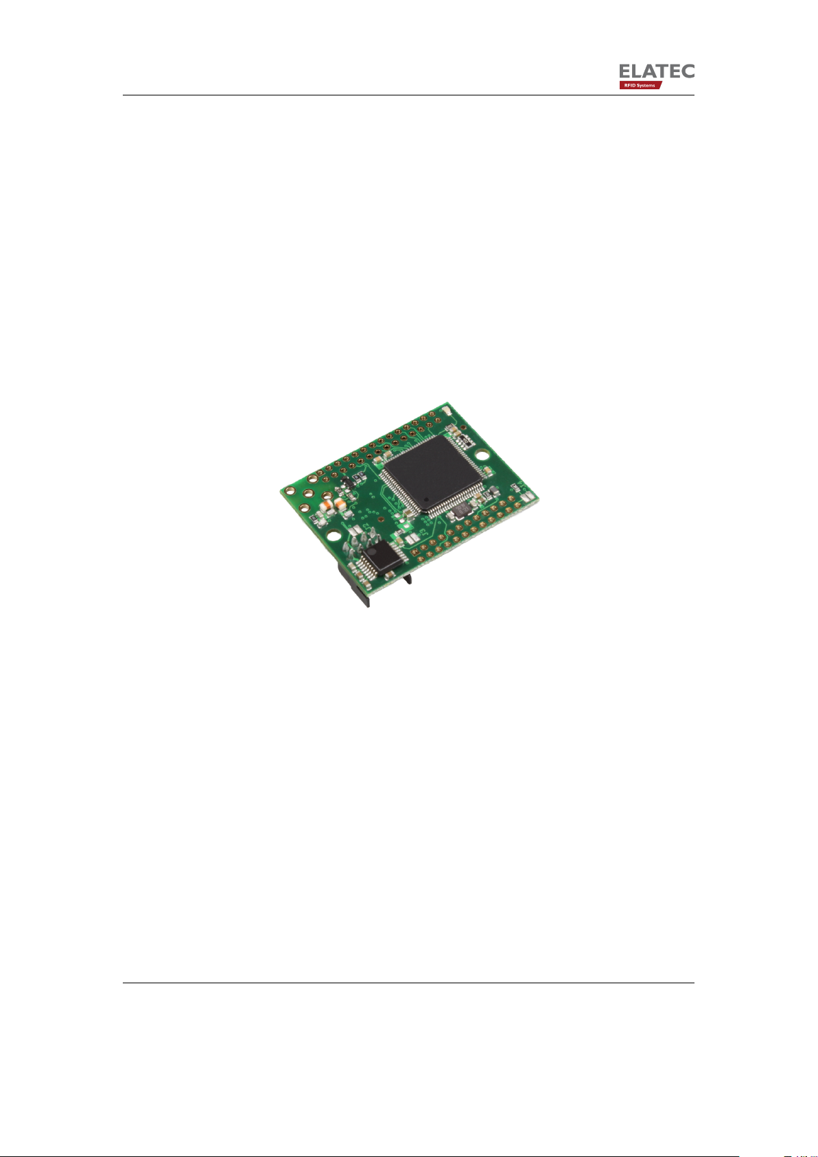
The TWN4 family of RFID readers/writers is built around the TWN4 Core Module.
Here is a picture of the TWN4 Core Module MIFARE NFC:
There are two different core modules available:
• TWN4 Core Module MIFARE NFC
• TWN4 Core Module LEGIC NFC
Page 5 of 36
Page 6
2 Products
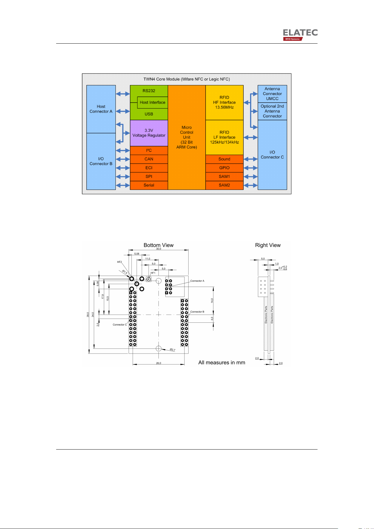
The core module contains voltage regulator, control unit, RFID front ends and communication interfaces.
2.1.1 Dimensions
The dimensions of TWN4 Core Module are as follows.:
2.1.2 Connectors
The TWN4 Core Module has several connectors on-board. There are three connectors (A, B
and C) which connect either to a carrier board or to a host. Furthermore, there is a antenna
connector and a optional position for placing a coaxial connector.
Page 6 of 36
Page 7
2 Products
The connectors A, B and C have identical pitch. Following type of connector is recommended:
• Dual row header
• Pitch 2.0mm
• Pin shape square
• Pin width 0.5mm x 0.5mm
• Length of pins appropriate to custom requirements
2.1.2.1 Connector A
The connector A is intended for connecting a cable to the TWN4 core module, which allows
communication with a host. Typically, such a cable is either type USB or RS232. Various
appropriate USB and RS232 cables are available from stock.
There is a right-angle connector mounted on-board, which is type Hirose, DF11 series.
Pin Pin Name Function
A1 UGND USB Ground
A2 USB_D+ USB Data +
A3 UVCC USB VCC
A4 USB_D- USB Data -
A5 V24_RXD RS232 RXD (Input)
A6 GND Ground
A7 V24_TXD RS232 TXD (Output)
A8 MGND Cable Sense
Note:
If pin A6 and A8 are connected to each other this has two effects:
1. The firmware of TWN4 changes host channel to RS232
2. The integrated circuit, which is interfacing to voltage levels of RS232 is powered up.
Following order codes for connector A and mating parts:
• Pin header on TWN4 Core Module: Hirose DF11-8DP-2DS(24)
• Mating part (crimping socket): Hirose DF11-8DS-2C
• Mating part (crimping contact): Hirose DF11-22SC (22 AWG)
Page 7 of 36
Page 8
2 Products
2.1.2.2 Connector B
Pin Pin Name Function
B1 GND Ground
B2 VIN Unregulated input to on-board voltage regulator
B3 VREG 3.3V output from on-board voltage regulator
B4 VCC 3.3V power supply input
B5 RESET- Low active TTL input with internal pull-up resistor
B6 PWRDWN- Low active TTL input with internal pull-up resistor
B7 COM1_RX- Low active TTL input with internal pull-up resistor
B8 COM1_TX- Low active TTL output (push/pull) of asyn-
B9 I2C_SDA Data pin of I2C interface. No internal pull up.
for hard reset.
for turning off the voltage regulator.
of asynchronous RXD to COM1.
chronous TXD from COM1.
B10 I2C_SCL Clock pin of I2C interface. No internal pull up.
B11 CAN_RX TTL RX pin of CAN interface. A external interface
circuit is required.
B12 CAN_TX TTL TX pin of CAN interface. A external interface
circuit is required.
B13 ECI_MOSI Pin MOSI of ECI
B14 ECI_MISO Pin MISO of ECI.
B15 ECI_CLK Pin CLK of ECI.
B16 ECI_ATTN- Pin ATTN- of ECI.
B17 GND Ground
B18 Res. This pin is reserved for future purposes.
B19 SPI_MOSI Pin MOSI of SPI interface
B20 SPI_MISO Pin MISO of SPI interface
B21 SPI_SCK Pin SCK of SPI interface
B22 SPI_SS- Pin SS- of SPI interface
B23 Res. This pin is reserved for future purposes.
B24 Res. This pin is reserved for future purposes.
Page 8 of 36
Page 9
2 Products
2.1.2.3 Connector C
Pin Pin Name Function
C1 GND Ground
C2 ANT_HF Together with pin C1, this pin builds a 50 ohm
C3 ANT_LF1 Output 1 for connecting external 125 kHz /
C4 ANT_LF2 Output 2 for connecting external 125 kHz /
C5 Res. This pin is reserved for future purposes.
C6 SPK+ Digitally modulated output for a speaker. Sec-
C7 IO0 GPIO0, I/O pin for general purposes.
output for connecting external 13.56MHz antennas
134.2 kHz antennas.
134.2 kHz antennas.
ond connection for the speaker is ground. The
impedance of the speaker should be greater than
24 ohm.
C8 IO1 GPIO1, I/O pin for general purposes.
C9 IO2 GPIO2, I/O pin for general purposes.
C10 IO3 GPIO3, I/O pin for general purposes.
C11 IO4 GPIO4, I/O pin for general purposes.
C12 IO5 GPIO5, I/O pin for general purposes.
C13 IO6 GPIO6, I/O pin for general purposes.
C14 IO7 GPIO7, I/O pin for general purposes.
C15 SAM1_CLK Clock output for SAM1
C16 GND Ground
C17 SAM1_IO I/O line for SAM1
C18 SAM1_RST Reset output for SAM1
C19 SAM2_CLK Clock output for SAM2
C20 GND Ground
C21 SAM2_IO I/O line for SAM2
C22 SAM2_RST Reset output for SAM2
continued on next page. . .
Page 9 of 36
Page 10
2 Products
Pin Pin Name Function
C23 COM2_RX- Low active TTL input with internal pull-up resistor
of asynchronous RXD to COM2.
C24 COM2_TX- Low active TTL output (push/pull) of asyn-
chronous TXD from COM2.
C25 Res. This pin is reserved for future purposes.
C26 Res. This pin is reserved for future purposes.
C27 Res. This pin is reserved for future purposes.
C28 VCC 3.3V power supply input or output for supplying
external components. Internally connected to B4.
Note:
• The nominal inductance for an external 125 kHz/134.2 kHz antenna is 490 µH. The
series resistance of the antenna should be lower than 10 ohms.
2.1.2.4 Connector HF1
HF connector 1 is a UMCC series 50-ohms output, which is connected internally in parallel
to pins C1 and C2.
2.1.2.5 Connector HF2
Position of HF2 offers the possibility to place another 50-ohm connector. It is connected
internally in parallel to pins C1 and C2. There are several series of RF connectors, which
can be used for position HF2, like SMA, SMB, SMC, MCX.
Page 10 of 36
Page 11

2 Products
2.1.3 Jumpers
There are several jumpers on-board of the TWN4 Core Module. Depending on the requirements these jumpers can be soldered together.
Jumper Function
J1 The function is identical to pins A6 and A8. If J1 is closed,
the RS232 interface is turned on and the host channel is
assumed to be RS232.
J2 Same function like J1 but other side of PCB.
J3 This jumper must be closed, if TWN4 Core Module is pow-
ered via connector A, e.g. from USB. It connects VCC from
the Core Module to the on-board voltage regulator, which is
supplied from connector A. If TWN4 Core Module is mounted
on a carrier board, this connection can be avoided by connecting pins B3 and B4 at the carrier board, which results in
exactly the same functionality.
J4 This jumper is for internal purposes only.
2.1.4 Power Supply
The picture below is showing, how power is routed through TWN4 Core Module:
Page 11 of 36
Page 12

2 Products
2.2 TWN4 OEM PCBs
An OEM PCB combines all components including antennas and core module, which are
required to build a full functional device. A OEM PCB consists of a carrier board, where
all other parts ar placed. Only cable and power supply is required to bring device into
operation.
Following OEM PCBs are available:
• TWN4 MIFARE NFC OEM PCB (Desktop)
• TWN4 LEGIC NFC OEM PCB (Desktop)
• TWN4 MIFARE NFC OEM PCB (Panel)
• TWN4 LEGIC NFC OEM PCB (Panel)
Page 12 of 36
Page 13

2 Products
2.2.1 TWN4 Desktop OEM PCB
Here is a picture of a TWN4 Desktop OEM PCB (it is a MIFARE NFC):
The block diagram looks as follows:
2.2.1.1 Dimensions & Pinout
The dimensions and pinout of TWN4 OEM PCB as follows.:
Page 13 of 36
Page 14

2 Products
Page 14 of 36
Page 15

2 Products
2.2.2 TWN4 Panel OEM PCB
Here is a picture of TWN4 Panel OEM PCB:
The block diagram looks as follows:
Page 15 of 36
Page 16

2 Products
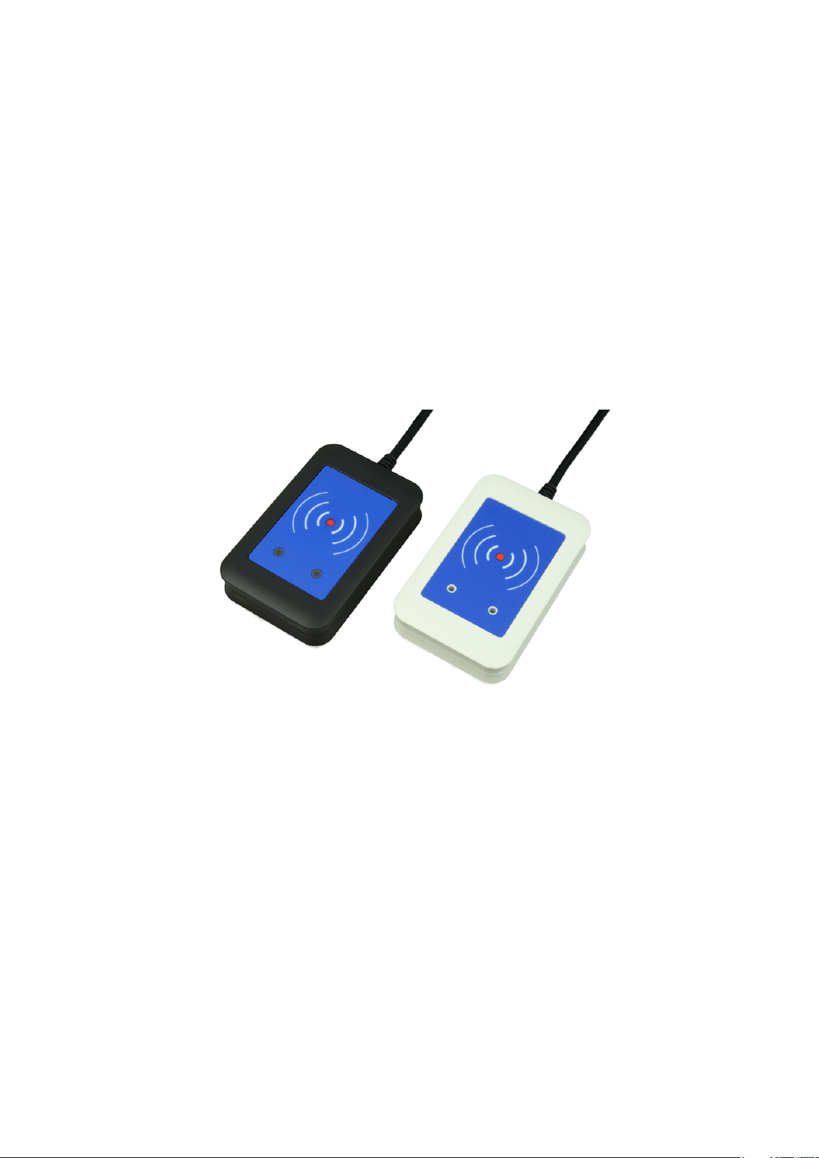
2.3 TWN4 Desktop
A TWN4 Desktop is a device, which contains TWN4 Desktop OEM PCB, housing and USB
or RS232 cable for host connection. It is available either in black or white.
2.4 TWN4 Mini Reader
TWN4 Mini Reader is a module to be integrated on custom PCB. It has a built-in HF antenna and subset of IOs compared to TWN4 Core Module. TWN4 Mini Reader is currently
available as version TWN4 Mini Reader MIFARE NFC.
Page 16 of 36
Page 17

2 Products
2.4.1 Connectors
The TWN4 Mini Reader has two on-board single row headers with 8 positions each. The
pins of these two connectors are together enumerated from 1 to 16.
• Single row header
• Pitch 2.54mm
• Pin shape square 0.635mm
Page 17 of 36
Page 18

2 Products
Pin Pin Name Function
1 RESET- Low active TTL input with internal pull-up resistor
for hard reset.
2 PWRDWN- Low active TTL input with internal pull-up resistor
for turning off the voltage regulator.
3 GND Ground
4 VIN Unregulated input to on-board voltage regulator
5 RXD- Low active TTL input with internal pull-up resistor
of asynchronous RXD to COM1.
6 TXD- Low active TTL output (push/pull) of asynchronous
TXD from COM1.
7 Res. Reserved for future use (intended for SCK from
SPI host interface).
8 Res. Reserved for future use (intended for SS- from SPI
host interface).
9 VCC Internaly regulated 3.0V power supply. To be used
for SAM1.
10 SAM_IO I/O line for SAM1.
11 GPIO3 GPIO3, I/O pin for general purposes.
12 GPIO2 GPIO2, I/O pin for general purposes.
13 GPIO1 GPIO1, I/O pin for general purposes.
14 GPIO0 GPIO0, I/O pin for general purposes.
15 SAM_CLK Clock output for SAM1
16 SAM_RST Reset output for SAM1
Page 18 of 36
Page 19

3 Firmware
3 Firmware
3.1 Memory View
The TWN4 Core Module has internal 256 kBytes of flash and 96 kBytes of RAM. The memory is devided into several sections as shown in the following diagram:
3.1.1 Boot Loader
The boot loader is the entry point for the firmware after powering up TWN4 or after a reset.
Only the boot loader provides functions for programming new firmware or Apps. This means
in order to program either a new firmware or another App, the boot loader must be entered.
3.1.2 Firmware
The firmware occupies most space in flash memory. It provides functions for accessing
IO or doing RFID operations. Furthermore, the execution of an App is controlled by the
firmware.
The firmware cannot be read back from a TWN4.
Page 19 of 36
Page 20

3 Firmware
3.1.3 App
The App is the part of flash memory, which specifies the behaviour of a TWN4. Due to this,
the programmer of the App has full control over the behaviour of the final application. An
App can be programmed by the customer. In order to do so, an appropriate developer pack
is provided.
An App cannot be read back from a TWN4. This allows to store secret keys and other
cryptographic functionality as part of an App. Furthermore, the possibility to clone a device
is avoided and the intellectual property is protected.
3.1.4 Storage
Storage is the section, where data is stored, which can be accessed via the storage functions. In other words, in this aera, the file system is located.
Page 20 of 36
Page 21

3 Firmware
3.2 Functional Units
Page 21 of 36
Page 22

3 Firmware
3.3 Firmware Startup Sequence
The diagram below is showing the sequence of how boot loader, firmware and App are
started:
3.4 Firmware Error Conditions
There are several reasons, because the firmware may run into a unwanted condition. If
this happens, the condition is shown by a on-board diagnostic red LED of the TWN4 Core
Module. The LED is signalling the error code by a number of flashes separated by a pause.
Page 22 of 36
Page 23

3 Firmware
This signalling is called blink code. Following blink codes are defined:
• Flash 1 time: There is no valid firmware installed on TWN4. This might be caused,
if programming a new firmware onto TWN4 is interrupted by a power failure. In this
case, the programming must be started from the beginning.
• Flash 2 times: There is no valid App installed on TWN4. This might be caused, if
programming a new App onto TWN4 is interrupted by a power failure. In this case, the
programming must be started from the beginning.
• Flash 3 times: The running App caused an exception. A exception is a invalid memory
access or invalid program instruction. An App is allowed to access it’s own memory
space only (64kByte ROM/64kByte RAM).
3.5 Backdoor for Starting the Boot Loader
During development of new Apps and under undefined circumstances, the situation might
arise, the starting the boot loader is not possible anymore. In such a situation, it is useful
to start the boot loader manually. This can be achieved by connecting two pins of the
TWN4 core module together and do a power cycle or reset. The two pins, which have to be
connected together are C25 and C28 of the TWN4 Core Module.
3.6 App & Firmware Images
Several firmware images are provided to the customer. App and firmware images can be
distginguished by the extension of their filename.
3.6.1 App Images
An App image has the extension .t4a. This extension replaces the older version .twn4.app,
which leaded to some inconvenience when sent through the Internet. After compiling source
code, the result is an App image with that extension. It can be programmed using AppBlaster
into TWN4.
3.6.2 Firmware Images
A firmware image has the extension .bix. Normally, such a file contains a firmware for TWN4
and an appropriate App for the intended purpose.
Page 23 of 36
Page 24

3 Firmware
3.6.2.1 Naming Scheme
There is a standard naming scheme for firmware images, which are given to the customer.
This is how the name of a firmware image is constructed:
Two types of hardware must be distinguished:
• ’C’, "Core Module": All products, which operate a TWN4 Core Module, like TWN4
Desktop, TWN4 OEM PCB, TWN4 Panel
• ’M’, "Mini Reader": This is related to the TWN4 Mini Reader only
There are several types of USB stacks available:
• ’K’: USB HID device (keyboard)
• ’C’: USB CDC device class (virtual COM port)
• ’H’: USB HID device (reports)
A USB stack is combined with an App. This might be either an App made by the customer
or an App provided by the manufacturer. Several Apps are available:
• "STD": Standard App, TWN4 is searching for transponder and forwarding the ID to
the host
• "PRS": Simple Protocol, TWN4 is running under the control by a host. TWN4 executes
commands, sent by the host and returns response. In this way, nearly all TWN4 system functions can be execute remotely by the host. There is separate documentation
and software available for using this mode of operation.
Page 24 of 36
Page 25

4 TWN4 Developer Pack
4 TWN4 Developer Pack
The TWN4 developer pack contains all software and documents necessary to operate, program and configure TWN4. Please see separate document for a detailed description of
the program AppBlaster, which is used to prepare TWN4 for operation according to your
requirements.
4.1 Installation
You received the TWN4 developer pack as zip file. In order to install the package, please
follow these steps:
• Create a empty directory on your hard disk
• Unzip the entire content of the zip file into this empty directory
• You’re done!
4.2 System Requirements
These are the minimum system requirements for a serious use of the TWN4 Developer
Pack:
• Operating system: Microsoft Windows XP or later, 32 or 64 bit
• Microsoft .NET Framework 3.5
• Processor (CPU): 2 GHz
• Hard Disk: 200 MB
• RAM: 2 GB
Page 25 of 36
Page 26

5 Compatibility
5 Compatibility
The table below is giving an overview about compatibility of TWN4 to various platforms and
their requirements.
System Mode Supported Driver Remark
Windows XP RS232 Yes Supported Port:
Windows 7 32/64 Bit by OS e.g. COM1:
Windows 8 32/64 Bit
USB HID Keyboard Yes Supported
by OS
USB CDC Yes Available Drivers are part
(Virtual COM Port) of the developer
pack
Linux 32/64 Bit RS232 Yes Supported Device:
(Ubuntu 10/11/12/13) by OS e.g. /dev/ttyS0
USB HID Keyboard Yes Supported
by OS
USB CDC Yes Supported Device:
(Virtual COM Port) by OS e.g. /dev/ttyACM0
Linux RS232 No N/A, platform
(ARM Platform) dependent
USB HID Keyboard Yes Supported
by OS
USB CDC Yes Supported Device
(Virtual COM Port) by OS e.g. /dev/ttyACM0
Windows CE RS232 Yes Supported Port:
by OS e.g. COM1:
USB HID Keyboard Yes Supported
by OS
USB CDC No N/A, platform
(Virtual COM Port) dependent
Page 26 of 36
Page 27

6 History of Changes
6 History of Changes
6.1 TWN4 Firmware
6.1.1 Firmware V1.23
• Initially released version.
6.1.2 Firmware V1.40
Firmware:
• LEGIC: System functions SM4200_xxx were renamed to SM4X00 due to support of
LEGIC chip SM4500 with identical API. Old style of functions is still available via
macros.
• LEGIC: New system functions for reprogramming OS of LEGIC SM4200 or SM4500.
• USB CDC: No modprobe required anymore under Linux.
• USB CDC: TWN4 is mounted as /dev/ttyACMx instead of /dev/ttyUSBx.
• New system functions Sleep, GetDeviceUID, SetParameters.
• Options to keep communication port closed in order to reduce power consumption.
• Option to start an App independent of the current USB enumeration status (standalone
applications).
• Support new USB class CCID in various flavours. Please contact your reseller for
these features.
• New API ISO7816 for accessing two SAM slots (e.g. on the TWN4 OEM PCB).
• Random number generator, which is available via read to CHANNEL_RNG.
• Support for new transponders: AWID, G-Prox, Pyramid and Keri.
• Reworked crypto API with new functionality for cyphered block chaining (CBC).
• Improved (parallel) reading of LF transponders.
Page 27 of 36
Page 28

6 History of Changes
• Cotag: Improved reading with the additional option to turn off verify, which further
speeds up recognition speed at still reliable reading performance
• Cotag: Decoded reading of ID data instead of a hash value.
• Inditag: Second read mode made available as known from TWN3 system function
IndiTagSearch2
• Honeytag: Decoded reading of ID data instead of a hash value.
• iCLASS: Support for SIO in a SAM slot.
• iCLASS: Support for reading of PAC from appropriate transponders.
• iCLASS: Support for iCLASS type ISO15693 in addition to ISO14443B.
• MIFARE NFC ISO15693: Improved reading performance.
• New API ISO14443 with new functions for transparent communication to transponder
types ISO14443A and ISO14443B.
6.1.3 Firmware V1.47
Firmware:
• Support NFC Peer-to-Peer
• Support ISO FDX-B
• Support EM4x50
• API for AT55xx
• Cotag: Improved reading including start bit
• G-Prox: Modified hash value for improved compatibility
• HITAG 2: Fix bug in Hitag2_SetPassword
• TIRIS: Relaxed read for better support of type multi page.
• App LEGIC Transparent: Support of digital I/O command
• App LEGIC Transparent: Receive-timeout of 1 second for messages
• App Tracer: Support new transponder types + receive of NDEF messages
• App Standard: Support new transponder types + receive of NDEF messages
Runtime environment:
• Optional definition of a manifest, which allows to modify parameters, before the App is
started.
Page 28 of 36
Page 29

6 History of Changes
• Functions memcmp, memcpy, memset are made available to Apps.
• Definition for NULL
• API for using the Simple Protocol from own Apps.
• Function SetHostChannel for redirecting output to other than default host port.
6.1.4 Firmware V1.48
Firmware:
• Mifare NFC: Support HF frontend V2
• Mifare NFC: Reset ATS incase of newly found transponder
• Fix issue in EM4150_WritePassword which caused an exception
• Cotag: Improved reading speed
• Cotag: Option for delivering 48 bits instead of 32 bits
Runtime environment:
• More flexible API for Simple Protocol including support of optional transmission of an
CRC
6.1.5 Firmware V1.49
Firmware:
• Mifare NFC: Hotfix for support of ISO15693
• Legic NFC: Hotfix for envelope command timeout issue
6.1.6 Firmware V1.57
Firmware:
• Support TWN4 Mini Reader Mifare NFC
• Support TWN4 SmartCard
• ISO7816: New system functions ISO7816_GetSlotStatus, ISO7816_IccPowerOn,
ISO7816_IccPowerOff
• ISO14443A: New system functions ISO14443A_GetATQA, ISO14443A_GetSAK
• ISO14443-4: Fix 14443-4 timeout issue
Page 29 of 36
Page 30

6 History of Changes
• ISO7816: Fix T=0 speed/timeout issue
• AT55xx: Fix support of bit rates below f/64
6.1.7 Firmware V1.64
• Hitag 1/S: Increased dynamic range
• Hitag 1/S, Hitag 2: Adjustable timing via parameters
• Hitag S: Read UID of transponders, which are operating in encrypted mode
• DESfire: System function DESfire_ChangeKey: Bugfix regarding PICCMasterKey and
Application MasterKey
• ISO14443B: Support transparent communication
• ISO14443B: New system functions ISO14443B_GetATQB, ISO14443B_GetAnswerToATTRIB
• ISO14443: Support high baudrates including parameters for setting up behaviour
• New system function GetLastError including error codes
• New API, which provides functions for access of internal flash storage
• MIFARE NFC: Improved reading of ISO15693
• Runtime lib: Systemfunctions HostTestCha r, HostWriteByte, HostReadByte are
now part of the runtime library
• Runtime lib: Changed naming scheme of all host communication functions by adding
a leading "Host"
• Runtime lib: HostWriteVersion can handle version strings with up to 50 characters
• ISO7816: Rework and improved API
• LEGIC NFC: Support of system functions ISO14443A_GetATS, ISO14443A_GetATQA,
ISO14443A_GetSAK
6.2 AppBlaster
6.2.1 AppBlaster V1.03
• Initially released version.
Page 30 of 36
Page 31

6 History of Changes
6.2.2 AppBlaster V1.40
• New work flow based on projects and templates.
• Save and load of projects.
• Support for all new transponder types of TWN4.
• Support for iCLASS PAC.
• Possibility to generate production images.
6.2.3 AppBlaster V1.47
• Support of new types of transponders including NFC
6.2.4 AppBlaster V1.49
• Support for Cotag 48 bits
6.2.5 AppBlaster V1.57
• Include correct App name and version into firmware image
• Support TWN4 Mini Reader Mifare NFC
6.2.6 AppBlaster V1.64
• Use of C99 language standard
6.3 Director
6.3.1 Director V1.00
• Initially released version.
Page 31 of 36
Page 32

6 History of Changes
6.3.2 Director V1.06
• Support system functions of TWN4 firmware V1.40
• Baud rate of serial communication can be adjusted
• "Simple Test": Selectable output format
• "Simple Test": Copy ID in clip board
• "Simple Test": Beep button is removed
• "Simple Test": Allow director to beep if needed
• "Simple Test": Only transponders, which are supported by TWN4 are selectable
• "Simple Test": Transponders, which are supported by TWN4 are selectable
• "Simple Test": Combo box is set up with currently configured transponders
• "Function Test": Possibility to enter a function call manually
6.3.3 Director V1.10
• Support of new transponder types and system functions according to TWN4 firmware
version 1.47.
• Support bytes arrays which contain 0(!) bytes
6.3.4 Director V1.11
• Improved GUI
• Support firmware V1.48
6.3.5 Director V1.12
• Improved communication interface
• Support firmware V1.49
6.3.6 Director V1.14
• Support firmware V1.57
• Support of Simple Protocol, ASCII or binary, with or without CRC
Page 32 of 36
Page 33

6 History of Changes
• Support of USB HID reports
• Support of TWN4 SmartCard (slot ID-1, ID-0/SAM, slot 3 and 4)
• Support extended version string (Core Module or Mini Reader)
6.3.7 Director V1.16
• Support firmware V1.64
• Resizeable and scrollable history list
• Defined minimum size of main window
• Improved connecting mechanism and behaviour
• Colourful feedback of result of call of system functions
• Simplification of entering parameters for structure TDESFireFileSettings
• Manual input of system calls
• Many minor improvements
6.4 General
6.4.1 TWN4DevPack147
• Stripped down tool chain
6.4.2 TWN4DevPack148
• Link of correct libgcc.a
Page 33 of 36
Page 34

7 Regulatory Information
7 Regulatory Information
7.1 FCC Statement
This device complies with Part 15 of the FCC rules. Operation is subject to the following
two conditions: (1) this device may not cause harmful interference, and (2) this device must
accept any interference received, including interference that may cause undesired operation.
Section 15.21 Information to user Changes or modifications not expressly approved by
the party responsible for compliance could void the user’s authority to operate the equipment
Section 15.105 (b) Note: This equipment has been tested and found to comply with the
limits for a Class B digital device, pursuant to part 15 of the FCC Rules. These limits
are designed to provide reasonable protection against harmful interference in a residential
installation. This equipment generates, uses and can radiate radio frequency energy and, if
not installed and used in accordance with the instructions, may cause harmful interference
to radio communications. However, there is no guarantee that interference will not occur in
a particular installation.
If this equipment does cause harmful interference to radio or television reception, which can
be determined by turning the equipment off and on, the user is encouraged to try to correct
the interference by one or more of the following measures:
• Reorient or relocate the receiving antenna.
• Increase the separation between the equipment and receiver.
• Connect the equipment into an outlet on a circuit different from that to which the receiver is connected.
• Consult the dealer or an experienced radio/TV technician for help.
7.2 IC (Industry Canada) Statement
This device complies with Industry Canada licence-exempt RSS standard(s). Operation is
subject to the following two conditions: (1) this device may not cause interference, and (2)
Page 34 of 36
Page 35

7 Regulatory Information
this device must accept any interference, including interference that may cause undesired
operation of the device.
Le présent appareil est conforme aux CNR d’Industrie Canada applicables aux appareils
radio exempts de licence. L’exploitation est autorisée aux deux conditions suivantes : (1)
l’appareil ne doit pas produire de brouillage, et (2) l’utilisateur de l’appareil doit accepter tout
brouillage radioélectrique subi, même si le brouillage est susceptible d’en compromettre le
fonctionnement.
Page 35 of 36
Page 36

8 Trademarks
8 Trademarks
All referenced brands, product names, service names and trademarks mentioned in this
document are the property of their respective owners.
Page 36 of 36
 Loading...