ELANT EL7512CY Datasheet

EL7512C - Preliminary
High Frequency PWM Step-Up Regulator
EL7512C - Preliminary
Features
• 90% efficiency
• Up to 600mA I
• 5V < V
OUT
OUT
< 18V
• VIN > 2V
• Up to 1.2MHz adjustable
frequency
• < 3µA shutdown current
• Adjustable soft-start
• Low battery detection
• Internal thermal protection
• 1.1mm max height 10-pin MSOP
package
Applications
• 3V to 5V, 12V, and 18V
converters
• 5V to 12V and 16V converters
• TFT-LCD
• DSL
• Portable equipment
• Desktop equipment
Ordering Information
Part No Package Tape & Reel Outline #
EL7512CY 10-Pin MSOP MDP0043
General Description
The EL7512C is a high frequency, high efficiency step-up DC:DC
regulator operated at fixed frequency PWM mode. With an integrated
1A MOSFET, it can deliver up to 600mA output current at up to 90%
efficiency. The adjustable switching frequency is up to 1.2MHz, making it ideal for DSL applications.
When shut down, it draws <3µA of current. This feature, along with
the minimum starting voltage of 2V, makes it suitable for portable
equipment powered by one lithium ion or 3 to 4 NiMH cells.
The EL7512C is available in a 10-pin MSOP package, with maximum
height of 1.1mm. With proper external components, the whole converter takes less than 0.25in2 PCB space.
This device is specified for operation over the full -40°C to +85°C
temperature range.
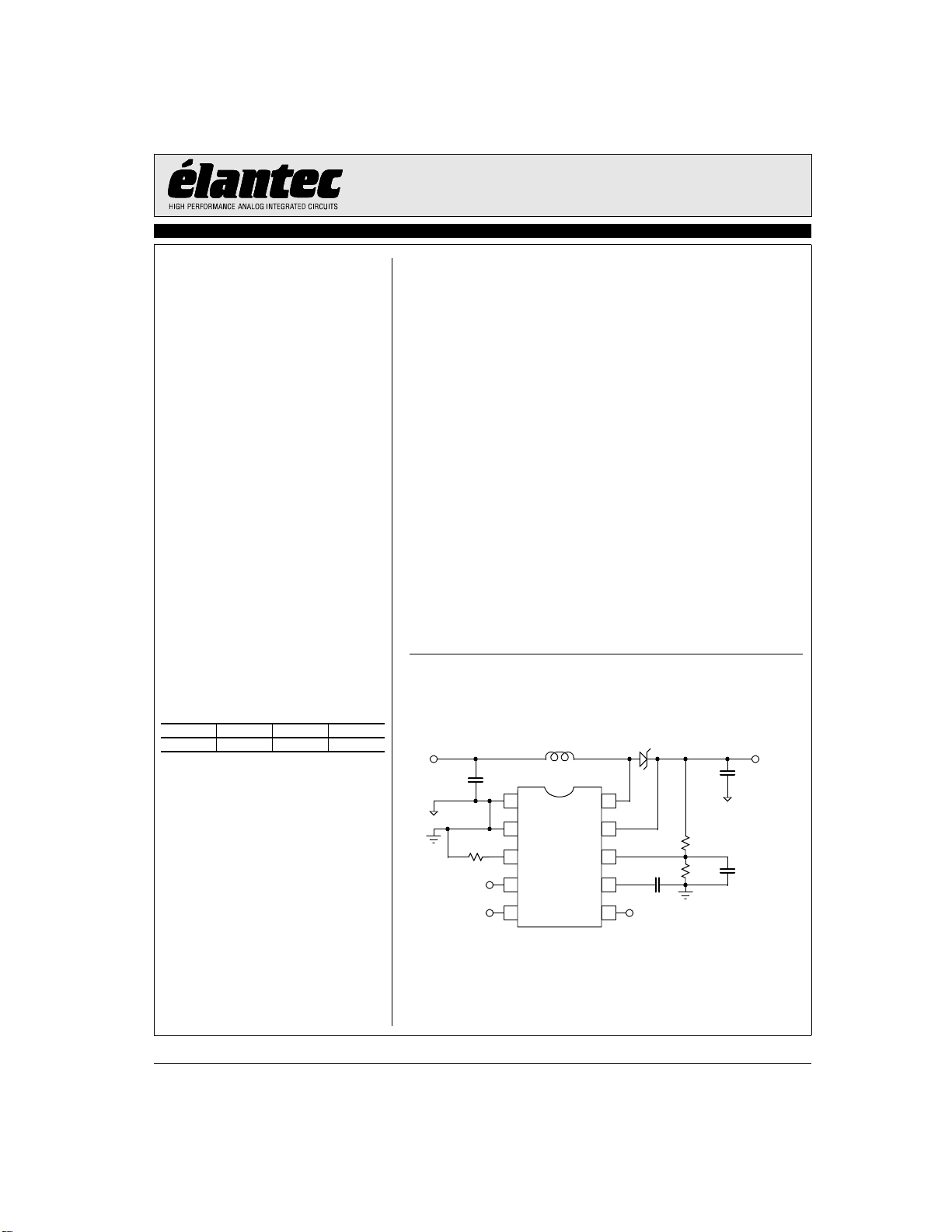
Typical Application Diagram
(2V-
9V)
V
IN
10µF
10µH
1
PGND
10
LX
47µF
V
OUT
(12V up
to
400mA)
2
SGND
100k
3
RT
4
EN
5 6
LBI
EL7512C
Note: All information contained in this data sheet has been carefully checked and is believed to be accurate as of the date of publication; however, this data sheet cannot be a “controlled document”. Current revisions, if any, to these
specifications are maintained at the factory and are available upon your request. We recommend checking the revision level before finalization of your design documentation.
© 2001 Elantec Semiconductor, Inc.
VDD
LBO
9
20nF
80.6kΩ
10kΩ 4.7nF
8
FB
7
SS
October 2, 2001

EL7512C - Preliminary
High Frequency PWM Step-Up Regulator
Absolute Maximum Ratings (T
Values beyond absolute maximum ratings can cause the device to be prematurely damaged. Absolute maximum ratings are stress ratings only
and functional device operation is not implied
VIN, LBI, V
EL7512C - Preliminary
Important Note:
All parameters having Min/Max specifications are guaranteed. Typ values are for information purposes only. Unless otherwise noted, all tests are at the
specified temperature and are pulsed tests, therefore: TJ = TC = T
DD
= 25°C)
A
A
+18V
LX Voltage 20V
Storage Temperature -65°C to +150°C
Operating Temperature -40°C to +85°C
Lead Temperature 300°C
Electrical Characteristics
VIN = 5V, V
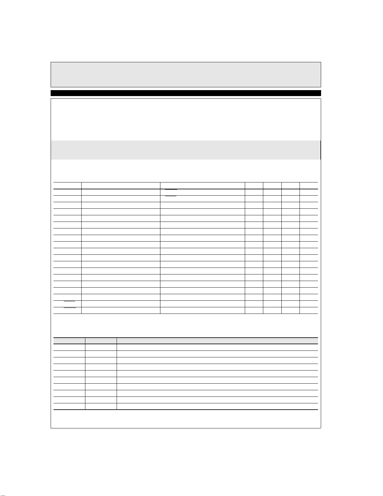
Parameter Description Condition Min Typ Max Unit
IQ1 Quiescent Current - Shut-down VSHDN = 0V 3 µA
IQ2 Quiensent Current VSHDN = 2V, Frequency = 600kHz 2.5 4 mA
VFB Feedback Voltage 1.31 1.35 1.39 V
IB Feedback Input Bias Current 0.10 µA
V
IN
D
MAX
I
LIM
I
SHDN
V
LBI
V
OL-LBO
I
LEAK-LBO
R
DS-ON
I
LEAK-SWITCH
∆V
OUT
∆V
OUT
F
OSC-RANGE
F
OSC1
VHI-SHDN SHDN Input High Threshold 1.6 V
VLO-SHDN SHDN Input Low Threshold 0.5 V
= 12V, I
OUT
Input Voltage Range 2 V
Maximum Duty Cycle 84 90 %
Current limit - Max Average Input Current 1000 1250 1500 mA
Shut-down Input Bias Current 1 µA
LBI Threshold Voltage 190 220 250 mV
LBO Output Low ILBO = 1mA 0.1 0.2 V
LBO Output Leakage Current VLBI = 250mV, VLBO = 5V 0.02 1 µA
Switch On Resistance at 12V output 300 mΩ
Switch Leakage Current 1 µA
/∆V
Line Regulation 3V < V
IN
/∆I
Load Regulation I
OUT
Frequency Range 1200 kHz
Switching Frequency R
OUT
= 0mA, F
= 600kHz, TA = 25°C unless otherwise specified.
OSC
< 6V, V
IN
< 250µA 0.5 1 %
OUT
= 100kΩ 530 670 800 kHz
OSC
OUT
= 12V, no load 0.15 %/V
Pin Descriptions
Pin Number Pin Name Pin Function
1 PGND Power ground; connected to the source of internal N-channel power MOSFET
2 SGND Signal ground; ground reference for all the control circuitry; needs to have only a single connection to PGND
3 RT Timing resister to adjust the oscillation frequency of the converter
4 EN Chip enable; connects to logic HI (>1.6V) for chip to function
5 LBI Low battery input; connects to a sensing voltage, or left open if function is not used
6 LBO Low battery detection output; connected to the open drain of a MOSFET; able to sink 1mA current
7 SS Soft-start; connects to a capacitor to control the start of the converter
8 FB Voltage feedback input; needs to connect to resistor divider to decide V
9 VDD Control circuit positive supply
10 LX Inductor drive pin; connected to the drain of internal N-channel power MOSFET
2
O

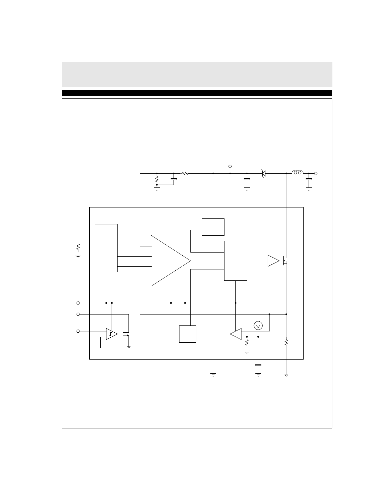
Block Diagram
EL7512C - Preliminary
High Frequency PWM Step-Up Regulator
V
OUT
80.6kΩ
10kΩ
4.7nF
FB VDD LX
15µF
EL7512C - Preliminary
V
IN
10µF47µF
100kΩ
LBO
LBI
MAX_DUTY
RT
Reference
Generator
EN
210mV
VREF
VRAMP
-
+
PWM
Comparato
Start-up
Oscillator
Thermal
Shut-down
PWM
Logic
-
+
I
LOUT
SGND PGNDSS
0.3Ω
12µA
80mΩ7.2k
20nF
3
 Loading...