EL5220C, EL5420C
12MHz Rail-to-Rail Input-Output Op Amps
EL5220C, EL5420C
Features
• 12MHz -3dB bandwidth
• Supply voltage = 4.5V to 16.5V
• Low supply current (per amplifier)
= 500µA
• High slew rate = 10V/µs
• Unity-gain stable
• Beyond the rails input capability
• Rail-to-rail output swing
• Ultra-small package
Applications
• TFT-LCD drive circuits
• Electronics notebooks
• Electronics games
• Touch-screen displays
• Personal communication devices
• Personal digital assistants (PDA)
• Portable instrumentation
• Sampling ADC amplifiers
• Wireless LANs
• Office automation
• Active filters
• ADC/DAC buffer
General Description
The EL5420C and EL5220C are low power, high voltage, rail-to-rail
input-output amplifiers. The EL5220C contains two amplifiers in one
package, and the EL5420C contains four amplifiers. Operating on supplies ranging from 5V to 15V, while consuming only 500µA per
amplifier, the EL5420C and EL5220C have a bandwidth of 12MHz --
(-3dB). They also provide common mode input ability beyond the supply rails, as well as rail-to-rail output capability. This enables these
amplifiers to offer maximum dynamic range at any supply voltage.
The EL5420C and EL5220C also feature fast slewing and settling
times, as well as a high output drive capability of 30mA (sink and
source). These features make these amplifiers ideal for use as voltage
reference buffers in Thin Film Transistor Liquid Crystal Displays
(TFT-LCD). Other applications include battery power, portable
devices, and anywhere low power consumption is important.
The EL5420C is available in a space-saving 14-pin TSSOP package,
the industry-standard 14-pin SO package, as well as a 16-pin LPP
package. The EL5220C is available in the 8-pin MSOP package. Both
feature a standard operational amplifier pin out. These amplifiers are
specified for operation over the full -40°C to +85°C temperature
range.
Connection Diagrams
1
VOUTA
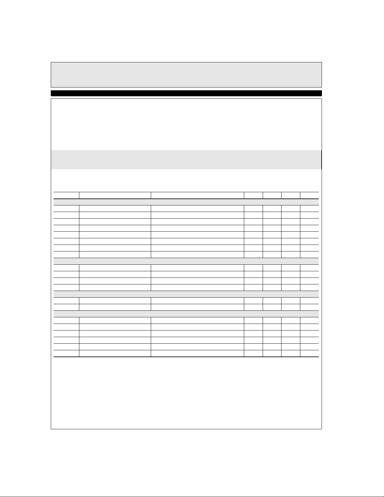
Ordering Information
Part No. Package
EL5220CY 8-Pin MSOP - MDP0043
EL5220CY-T7 8-Pin MSOP 7” MDP0043
EL5220CY-T13 8-Pin MSOP 13” MDP0043
EL5420CL 16-Pin LPP - MDP0046
EL5420CL-T7 16-Pin LPP 7” MDP0046
EL5420CL-T13 16-Pin LPP 13” MDP0046
EL5420CR 14-Pin TSSOP - MDP0044
EL5420CR-T7 14-Pin TSSOP 7” MDP0044
EL5420CR-T13 14-Pin TSSOP 13” MDP0044
EL5420CS 14-Pin SO - MDP0027
EL5420CS-T7 14-Pin SO 7” MDP0027
EL5420CS-T13 14-Pin SO 13” MDP0027
Note: All information contained in this data sheet has been carefully checked and is believed to be accurate as of the date of publication; however, this data sheet cannot be a “controlled document”. Current revisions, if any, to these
specifications are maintained at the factory and are available upon your request. We recommend checking the revision level before finalization of your design documentation.
© 2001 Elantec Semiconductor, Inc.
Tape &
Reel Outline #
2
VINA-
VINA+
VINB+
VINB-
VOUTB
Connection Diagrams are continued on page 4
-
3
+
4
5
+
6
-
7
EL5420C
(14-Pin TSSOP & 14-Pin SO)
14
VOUTD
13
VIND-
12
+
VIND+
1
11
VS-VS+
10
VINC+
+
9
-
VINC-
8
VOUTC
VOUTA
VINA-
VINA+
VS-
2
3
4
+
EL5220C
(8-Pin MSOP)
8
VS+
7
VOUTB
65-
VINB-
+
VINB+
September 19, 2001

EL5220C, EL5420C
12MHz Rail-to-Rail Input-Output Op Amps
Absolute Maximum Ratings (T
Values beyond absolute maximum ratings can cause the device to be prematurely damaged. Absolute maximum ratings are stress ratings only
EL5220C, EL5420C
and functional device operation is not implied
Supply Voltage between VS+ and VS- +18V
Input Voltage VS- - 0.5V, VS +0.5V
Maximum Continuous Output Current 30mA
= 25°C)
A
Maximum Die Temperature +125°C
Storage Temperature -65°C to +150°C
Operating Temperature -40°C to +85°C
Power Dissipation See Curves
ESD Voltage 2kV
Important Note:
All parameters having Min/Max specifications are guaranteed. Typ values are for information purposes only. Unless otherwise noted, all tests are at the
specified temperature and are pulsed tests, therefore: TJ = TC = T
A
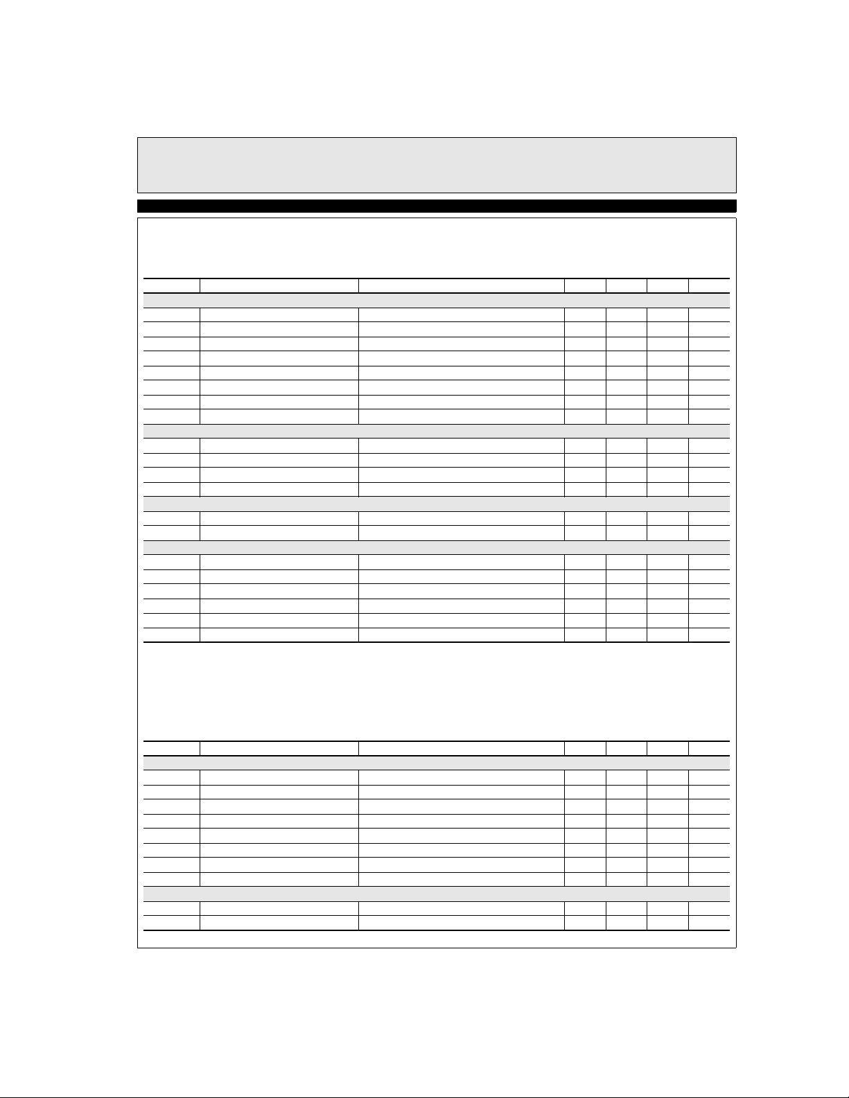
Electrical Characteristics
VS+= +5V, VS - = -5V, R
Parameter Description Condition Min Typ Max Unit
Input Characteristics
V
OS
TCV
OS
I
B
R
IN
C
IN
CMIR Common-Mode Input Range -5.5 +5.5 V
CMRR Common-Mode Rejection Ratio for VIN from -5.5V to +5.5V 50 70 dB
A
VOL
Output Characteristics
V
OL
V
OH
I
SC
I
OUT
Power Supply Performance
PSRR Power Supply Rejection Ratio VS is moved from ±2.25V to ±7.75V 60 80 dB
I
S
Dynamic Performance
SR Slew Rate
t
S
BW -3dB Bandwidth R
GBWP Gain-Bandwidth Product R
PM Phase Margin R
CS Channel Separation f = 5MHz 75 dB
1. Measured over operating temperature range
2. Slew rate is measured on rising and falling edges
= 10kΩ and C
L
Input Offset Voltage V
Average Offset Voltage Drift
Input Bias Current V
= 10pF to 0V, TA = 25°C unless otherwise specified.
L
= 0V 2 12 mV
CM
[1]
= 0V 2 50 nA
CM
5 µV/°C
Input Impedance 1 GΩ
Input Capacitance 1.35 pF
Open-Loop Gain -4.5V ≤ V
≤ +4.5V 75 95 dB
OUT
Output Swing Low IL = -5mA -4.92 -4.85 V
Output Swing High IL = 5mA 4.85 4.92 V
Short Circuit Current ±120 mA
Output Current ±30 mA
Supply Current (Per Amplifier) No load 500 750 µA
[2]
-4.0V ≤ V
≤ +4.0V, 20% to 80% 10 V/µs
OUT
Settling to +0.1% (AV = +1) (AV = +1), VO = 2V step 500 ns
= 10kΩ, C
L
= 10kΩ, C
L
= 10kΩ, C
L
= 10pF 12 MHz
L
= 10pF 8 MHz
L
= 10 pF 50 °
L
2

EL5220C, EL5420C
12MHz Rail-to-Rail Input-Output Op Amps
Electrical Characteristics
VS+ = 5V, VS-= 0V, R
Parameter Description Condition Min Typ Max Unit
Input Characteristics
V
OS
TCV
OS
I
B
R
IN
C
IN
CMIR Common-Mode Input Range -0.5 +5.5 V
CMRR Common-Mode Rejection Ratio for VIN from -0.5V to +5.5V 45 66 dB
A
VOL
Output Characteristics
V
OL
V
OH
I
SC
I
OUT
Power Supply Performance
PSRR Power Supply Rejection Ratio VS is moved from 4.5V to 15.5V 60 80 dB
I
S
Dynamic Performance
SR Slew Rate
t
S
BW -3dB Bandwidth R
GBWP Gain-Bandwidth Product R
PM Phase Margin R
CS Channel Separation f = 5MHz 75 dB
1. Measured over operating temperature range
2. Slew rate is measured on rising and falling edges
= 10kΩ and C
L
Input Offset Voltage V
Average Offset Voltage Drift
Input Bias Current V
= 10pF to 2.5V, TA = 25°C unless otherwise specified.
L
= 2.5V 2 10 mV
CM
[1]
= 2.5V 2 50 nA
CM
5 µV/°C
Input Impedance 1 GΩ
Input Capacitance 1.35 pF
Open-Loop Gain 0.5V ≤ V
≤+ 4.5V 75 95 dB
OUT
Output Swing Low IL = -5mA 80 150 mV
Output Swing High IL = +5mA 4.85 4.92 V
Short Circuit Current ±120 mA
Output Current ±30 mA
Supply Current (Per Amplifier) No load 500 750 µA
[2]
1V ≤ V
≤ 4V, 20% to 80% 10 V/µs
OUT
Settling to +0.1% (AV = +1) (AV = +1), VO = 2V step 500 ns
= 10kΩ, C
L
= 10 kΩ, C
L
= 10 kΩ, C
L
= 10pF 12 MHz
L
= 10pF 8 MHz
L
= 10 pF 50 °
L
EL5220C, EL5420C
Electrical Characteristics
VS+ = 15V, VS- = 0V, R
Parameter Description Condition Min Typ Max Unit
Input Characteristics
V
OS
TCV
OS
I
B
R
IN
C
IN
CMIR Common-Mode Input Range -0.5 +15.5 V
CMRR Common-Mode Rejection Ratio for VIN from -0.5V to +15.5V 53 72 dB
A
VOL
Output Characteristics
V
OL
V
OH
= 10kΩ and C
L
Input Offset Voltage V
Average Offset Voltage Drift
Input Bias Current V
= 10pF to 7.5V, TA = 25°C unless otherwise specified.
L
= 7.5V 2 14 mV
CM
[1]
= 7.5V 2 50 nA
CM
5 µV/°C
Input Impedance 1 GΩ
Input Capacitance 1.35 pF
Open-Loop Gain 0.5V ≤ V
≤ 14.5V 75 95 dB
OUT
Output Swing Low IL = -5mA 80 150 mV
Output Swing High IL = +5mA 14.85 14.92 V
3

EL5220C, EL5420C
12MHz Rail-to-Rail Input-Output Op Amps
Electrical Characteristics (Continued)
VS+ = 15V, VS- = 0V, R
Parameter Description Condition Min Typ Max Unit
EL5220C, EL5420C
I
SC
I
OUT
Power Supply Performance
PSRR Power Supply Rejection Ratio VS is moved from 4.5V to 15.5V 60 80 dB
I
S
Dynamic Performance
SR Slew Rate
t
S
BW -3dB Bandwidth R
GBWP Gain-Bandwidth Product R
PM Phase Margin R
CS Channel Separation f = 5MHz 75 dB
1. Measured over operating temperature range
2. Slew rate is measured on rising and falling edges
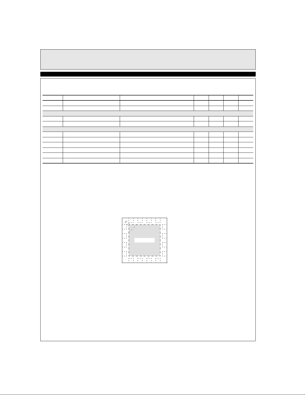
Connection Diagrams (Continued)
= 10kΩ and C
L
= 10pF to 7.5V, TA = 25°C unless otherwise specified.
L
Short Circuit Current ±120 mA
Output Current ±30 mA
Supply Current (Per Amplifier) No load 500 750 µA
[2]
1V ≤ V
≤ 14V, 20% to 80% 10 V/µs
OUT
Settling to +0.1% (AV = +1) (AV = +1), VO = 2V step 500 ns
= 10kΩ, C
L
= 10kΩ, C
L
= 10kΩ, C
L
= 10pF 12 MHz
L
= 10pF 8 MHz
L
= 10 pF 50 °
L
VINA-
VINA+
VS+
VINB+
NC
VOUTA
VOUTD
16
15
1
2
Thermal Pad
3
4
5
6
VINB-
VOUTB
EL5420C
(16-Pin LPP)
NC
14
13
12
VIND-
11
VIND+
10
VS-
9
VINC+
7
8
VINC-
VOUTC
4
 Loading...