ELANT EL5410CR-T13, EL5410CR, EL5210CY-T7, EL5210CY-T13, EL5210CY Datasheet
...
EL5210C/EL5410C
30MHz Rail-to-Rail Input-Output Op Amps
EL5210C/EL5410C
Features
• 30MHz -3dB bandwidth
• Supply voltage = 4.5V to 16.5V
• Low supply current (per amplifier)
= 2.5mA
• High slew rate = 33V/µs
• Unity-gain stable
• Beyond the rails input capability
• Rail-to-rail output swing
• Available in both standard and
space-saving fine pitch packages
Applications
• Driver for A-to-D Converters
• Data Acquisition
• Video Processing
• Audio Processing
• Active Filters
• Tes t Equi p ment
• Battery Powered Applications
• Portable Equipment
Ordering Information
Part No. Package Tape & Re el Outline #
EL5210CS 8-Pin SOIC - MDP0027
EL5210CS-T13 8-Pin SOIC 13” MDP0027
EL5210CY 8-Pin MSOP - MDP0043
EL5210CY-T7 8-Pin MSOP 7” MDP0043
EL5210CY-T13 8-Pin MSOP 13” MDP0043
EL5410CS 14-Pin SOIC - MDP0027
EL5410CS-T13 14-Pin SOIC 13” MDP0027
EL5410CR 14-Pin TSSOP - MDP0044
EL5410CR-T13 14-Pin TSSOP 13” MDP0044
General Description
The EL5210C and EL5410C are low power, high voltage rail-to-rail
input-output amplifiers. The EL5210C contains two amplifiers in one
package and the EL5410C contains four amplifiers. Operating on supplies ranging from 5V to 15V, while consuming only 2.5mA per
amplifier, the EL5410C and EL5210C have a bandwidth of 30MHz --
(-3dB). They also provide common mode input ability beyond the supply rails, as well as rail-to-rail output capability. This enables these
amplifiers to offer maximum dynamic range at any supply voltage.
The EL5410C and EL5210C also feature fast slewing and settling
times, as well as a high output drive capability of 30mA (sink and
source). These features make these amplifiers ideal for high speed filtering and signal conditioning application. Other applications include
battery power, portable devices, and anywhere low power consumption is important.
The EL5410C is available in a space-saving 14-Pin TSSOP package,
as well as the industry-standard 14-Pin SOIC. The EL5210C is available in the 8-Pin MSOP and 8-Pin SOIC packages. Both feature a
standard operational amplifier pin out. These amplifiers operate over a
temperature range of -40°C to +85°C.
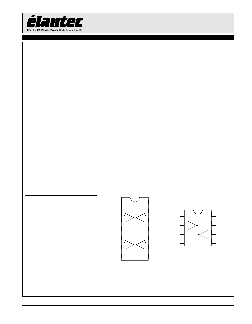
Connection Diagram
VOUTA
1
VINA-
2
VINA+
VINB+
VINB-
VOUTB
-
3
+
4
5
+
6
-
7
EL5410C (TSSOP-14, SOIC-14)
VOUTD
14
VIND-
13
-
VIND+
12
+
11
VS-VS+
VINC+
10
+
VINC-
9
-
VOUTC
8
1
VOUTA
2
VINA-
VINA+
-
+
3
4
VS-
EL5210C (MSOP-8, SOIC-8)
8
VS+
7
VOUTB
6
-
VINB-
+
5
VINB+
November 16, 2000
Note: All information contained in this data sheet has been carefully checked and is believed to be accurate as of the date of publication; however, this data sheet cannot be a “controlled document”. Current revisions, if any, to these
specifications are maintained at the factory and are available upon your request. We recommend checking the revision level before finalization of your design documentation.
© 2000 Elantec Semiconductor, Inc.
EL5210C/EL5410C
30MHz Rail-to-Rail Input-Output Op Amps
Absolute Maximum Ratings (T
Values beyond absolute maximum ratings can cause the device to be prematurely damaged. Absolute maximum ratings are stress ratings only and
EL5210C/EL5410C
functional device operation is not implied.
Supply Voltage between V
Input Voltage V
Maximum Continuous Output Current 30mA
+ and VS- +18V
S
= 25°C)
A
- - 0.5V, VS +0.5V
S
Maximum Die Temperature +125°C
Storage Temperature -65°C to +150°C
Operating Temperature -40°C to +85°C
Power Dissipation See Curves
ESD Voltage 2kV
Important Note:
All parameters having Min/Max specifications are guaranteed. Typ values are for information purposes only. Unless otherwise noted, all tests are at the
specified temperature and are pulsed tests, therefore: T
= TC = T
J
A
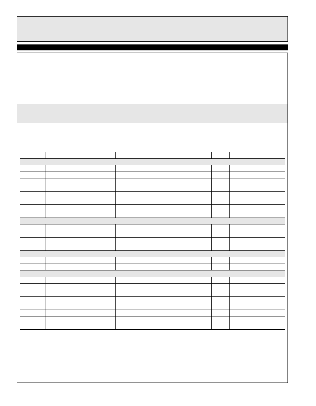
Electrical Characteristics
VS+ = +5V, VS - = -5V, RL = 1kΩ and CL = 12pF to 0V, TA = 25°C unless otherwise specified.
Parameter Description Condition Min Typ Max Unit
Input Characteristics
V
OS
TCV
I
B
R
IN
C
IN
CMIR Common-Mode Input Range -5.5 +5.5 V
CMRR Common-Mode Rejection Ratio for V
A
VOL
Output Characteristics
V
OL
V
OH
I
SC
I
OUT
Power Supply Performance
PSRR Power Supply Rejection Ratio V
I
S
Dynamic Performance
SR Slew Rate
t
S
BW -3dB Bandwidth 30 MHz
GBWP Gain-Bandwidth Product 20 MHz
PM Phase Margin 50 °
CS Channel Separation f = 5MHz 110 dB
d
G
d
P
1. Measured over operating temperature range
2. Slew rate is measured on rising and falling edges
3. NTSC signal generator used
Input Offset Voltage V
Average Offset Voltage Drift
OS
Input Bias Current V
[1]
= 0V 3 15 mV
CM
7µV/°C
= 0V 2 60 nA
CM
Input Impedance 1GΩ
Input Capacitance 2pF
from -5.5V to 5.5V 50 70 dB
Open-Loop Gain -4.5V ≤ V
IN
≤ 4.5V 65 80 dB
OUT
Output Swing Low IL = -5mA -4.9 -4.8 V
Output Swing High IL = 5mA 4.8 4.9 V
Short Circuit Current ±120 mA
Output Current ±30 mA
is moved from ±2.25V to ±7.75V 60 80 dB
S
Supply Current (Per Amplifier) No Load 2.5 3.75 mA
[2]
-4.0V ≤ V
≤ 4.0V, 20% o 80% 33 V/µs
OUT
Settling to +0.1% (AV = +1) (AV = +1), VO = 2V Step 140 ns
Differential Gain
Differential Phase
[3]
[3]
RF = RG = 1kΩ and V
RF = RG = 1kΩ and V
= 1.4V 0.12 %
OUT
= 1.4V 0.17 °
OUT
2
EL5210C/EL5410C
30MHz Rail-to-Rail Input-Output Op Amps
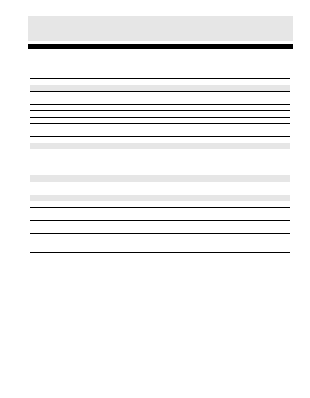
Electrical Characteristics
VS+ = 5V, VS- = 0V, RL = 1kΩ and CL = 12pF to 2.5V, TA = 25°C unless otherwise specified.
Parameter Description Condition Min Typ Max Unit
Input Characteristics
V
OS
TCV
OS
I
B
R
IN
C
IN
CMIR Common-Mode Input Range -0.5 +5.5 V
CMRR Common-Mode Rejection Ratio for V
A
VOL
Output Characteristics
V
OL
V
OH
I
SC
I
OUT
Power Supply Performance
PSRR Power Supply Rejection Ratio V
I
S
Dynamic Performance
SR Slew Rate
t
S
BW -3dB Bandwidth 30 MHz
GBWP Gain-Bandwidth Product 20 MHz
PM Phase Margin 50 °
CS Channel Separation f = 5MHz 110 dB
d
G
d
P
1. Measured over operating temperature range
2. Slew rate is measured on rising and falling edges
3. NTSC signal generator used
Input Offset Voltage V
Average Offset Voltage Drift
[1]
Input Bias Current V
= 2.5V 3 15 mV
CM
7µV/°C
= 2.5V 2 60 nA
CM
Input Impedance 1GΩ
Input Capacitance 2pF
from -0.5V to 5.5V 45 66 dB
Open-Loop Gain 0.5V ≤ V
IN
≤ 4.5V 65 80 dB
OUT
Output Swing Low IL = -5mA 100 200 mV
Output Swing High IL = 5mA 4.8 4.9 V
Short Circuit Current ±120 mA
Output Current ±30 mA
is moved from 4.5V to 15.5V 60 80 dB
S
Supply Current (Per Amplifier) No Load 2.5 3.75 mA
[2]
1V ≤ V
≤ 4V, 20% o 80% 33 V/µs
OUT
Settling to +0.1% (AV = +1) (AV = +1), VO = 2V Step 140 ns
Differential Gain
Differential Phase
[3]
[3]
RF = RG = 1kΩ and V
RF = RG = 1kΩ and V
= 1.4V 0.30 %
OUT
= 1.4V 0.66 °
OUT
EL5210C/EL5410C
3
EL5210C/EL5410C
30MHz Rail-to-Rail Input-Output Op Amps
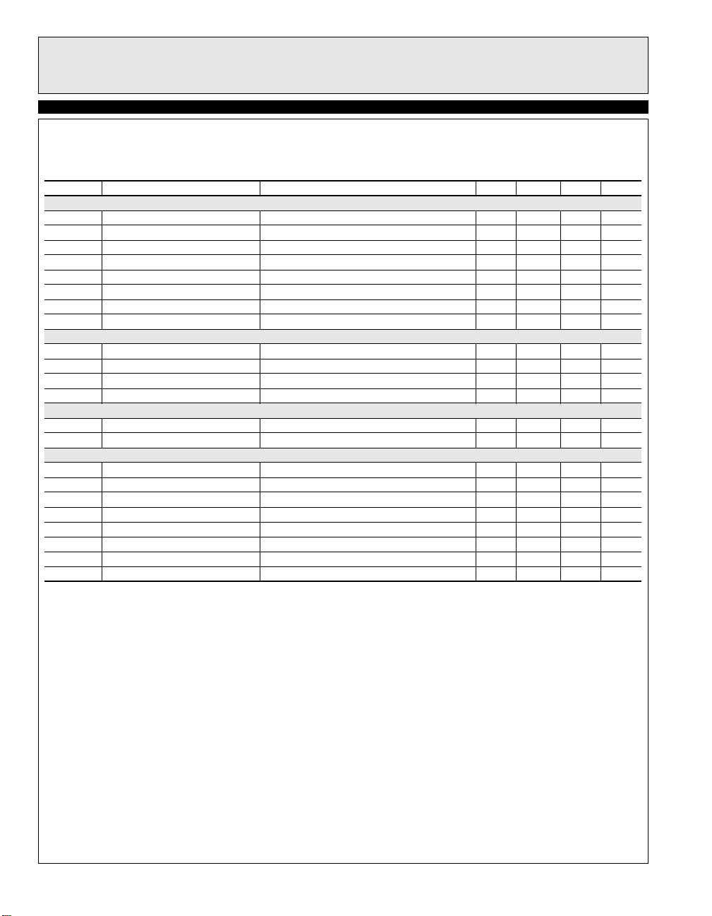
Electrical Characteristics
VS+ = 15V, VS- = 0V, RL = 1kΩ and CL = 12pF to 7.5V, TA = 25°C unless otherwise specified.
EL5210C/EL5410C
Parameter Description Condition Min Typ Max Unit
Input Characteristics
V
OS
TCV
I
B
R
IN
C
IN
CMIR Common-Mode Input Range -0.5 +15.5 V
CMRR Common-Mode Rejection Ratio for V
A
VOL
Output Characteristics
V
OL
V
OH
I
SC
I
OUT
Power Supply Performance
PSRR Power Supply Rejection Ratio V
I
S
Dynamic Performance
SR Slew Rate
t
S
BW -3dB Bandwidth 30 MHz
GBWP Gain-Bandwidth Product 20 MHz
PM Phase Margin 50 °
CS Channel Separation f = 5MHz 110 dB
d
G
d
P
1. Measured over operating temperature range
2. Slew rate is measured on rising and falling edges
3. NTSC signal generator used
Input Offset Voltage V
Average Offset Voltage Drift
OS
Input Bias Current V
[1]
= 7.5V 3 15 mV
CM
7µV/°C
= 7.5V 2 60 nA
CM
Input Impedance 1GΩ
Input Capacitance 2pF
from -0.5V to 15.5V 53 72 dB
Open-Loop Gain 0.5V ≤ V
IN
≤ 14.5V 65 80 dB
OUT
Output Swing Low IL = -7.5mA 170 350 mV
Output Swing High IL = 7.5mA 14.65 14.83 V
Short Circuit Current ±120 mA
Output Current ±3 0 mA
is moved from 4.5V to 15.5V 60 80 dB
S
Supply Current (Per Amplifier) No Load 2.5 3.75 mA
[2]
1V ≤ V
≤ 14V, 20% o 80% 33 V/µ s
OUT
Settling to +0.1% (AV = +1) (AV = +1), VO = 2V Step 140 n s
Differential Gain
Differential Phase
[3]
[3]
RF = RG = 1kΩ and V
RF = RG = 1kΩ and V
= 1.4V 0.10 %
OUT
= 1.4V 0.11 °
OUT
4
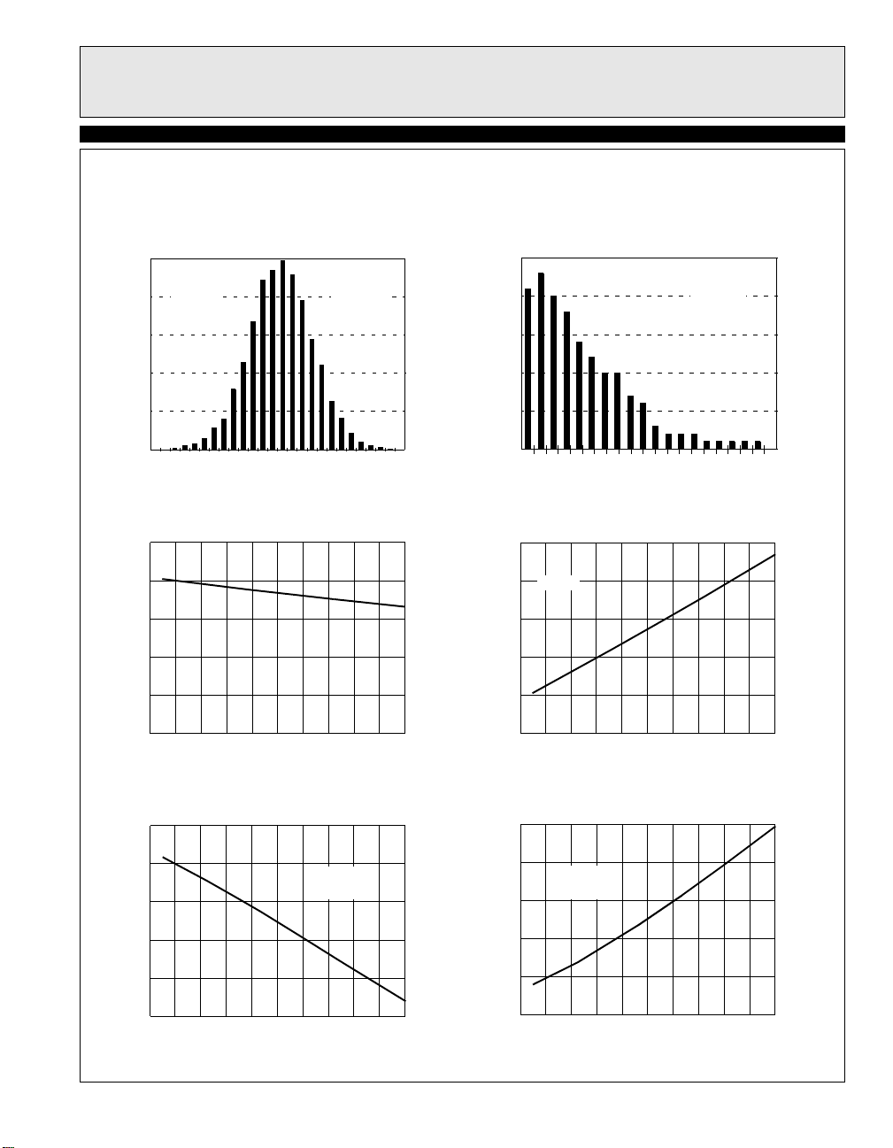
Typical Performance Curves
EL5210C/EL5410C
EL5210C/EL5410C
30MHz Rail-to-Rail Input-Output Op Amps
EL5410C Input Offset Voltage Distribution
500
246
Typical
Production
Distortion
VS=±5V
T
=25°C
A
400
300
200
Quantity (Amplifiers)
100
0
5
4
3
2
Input Offset Voltage (mV)
1
0
-8-6-4-2-0
-12
-10
Input Offset Voltage (mV)
Input Offset Voltage vs Temperature
-50 -10 30 70 110 150
Temperature (°C)
EL5410C Input Offset Voltage Drift
25
VS=±5V
20
15
10
Quantity (Amplifiers)
5
8
10
12
0
1
3
5
7
9
Input Offset Voltage Drift, TCVOS(µV/°C)
Input Bias Current vs Temperature
0.008
0.004
VS=±5V
0
-0.004
Input Bias Current (µA)
-0.008
-0.012
-50 -10 30 70 110 150
Temperature (°C)
Typical
Production
Distortion
11
13
15
17
19
21
Output High Voltage vs Temperature
4.96
4.95
4.94
4.93
Output High Voltage (V)
4.92
4.91
-50 -10 30 70 110 150
Temperature (°C)
VS=±5V
I
OUT
=5mA
Output Low Voltage vs Temperature
-4.85
-4.87
-4.89
-4.91
Output Low Voltage (V)
-4.93
-4.95
VS=±5V
I
=5mA
OUT
-50 -10 30 70 110 150
Temperature (°C)
5
 Loading...