ELANT EL5292CS-T7, EL5292CS-T13, EL5292CS Datasheet
EL5292C
Dual 600MHz Current Feedback Amplifier
EL5292C
Features
• 600MHz -3dB band w idth
• 6mA supply current (per amplifier)
• Single and dual sup p l y op er a tion,
from 5V to 10V
• Single (EL5192C) and triple
(EL5392C) available
• High speed, 1GHz product
available (EL519 1C )
• Low power, 4mA, 300MHz
product available (EL5193C,
EL5293C, and EL5393C
Applications
• Video Amplifiers
• Cable Drivers
• RGB Amplifiers
• Test Equipment
• Instrumentation
• Current to Voltage Converters
Ordering Information
Part No Package
EL5292CS 8-Pin SO - MDP0027 EL5292CS-T7 8-Pin SO 7” MDP0027 EL5292CS-T13 8-Pin SO 13” MDP0027
Tape &
Reel Outline #
General Description
The EL5292C is a dual current feedback amplifier with a very h igh
bandwidth of 600MHz. This makes this amplifier ideal for today’s
high speed video and monitor applications .
With a supply current of just 6mA per amplifier and the ability to run
from a single supply voltage from 5V to 10V, the EL5292C is also
ideal for hand held, portable or battery powered equipment.
The EL5292C is offered in the industry standard 8-pin SO. The
EL5292C operates over the industrial temperature range of -40°C to
+85°C.
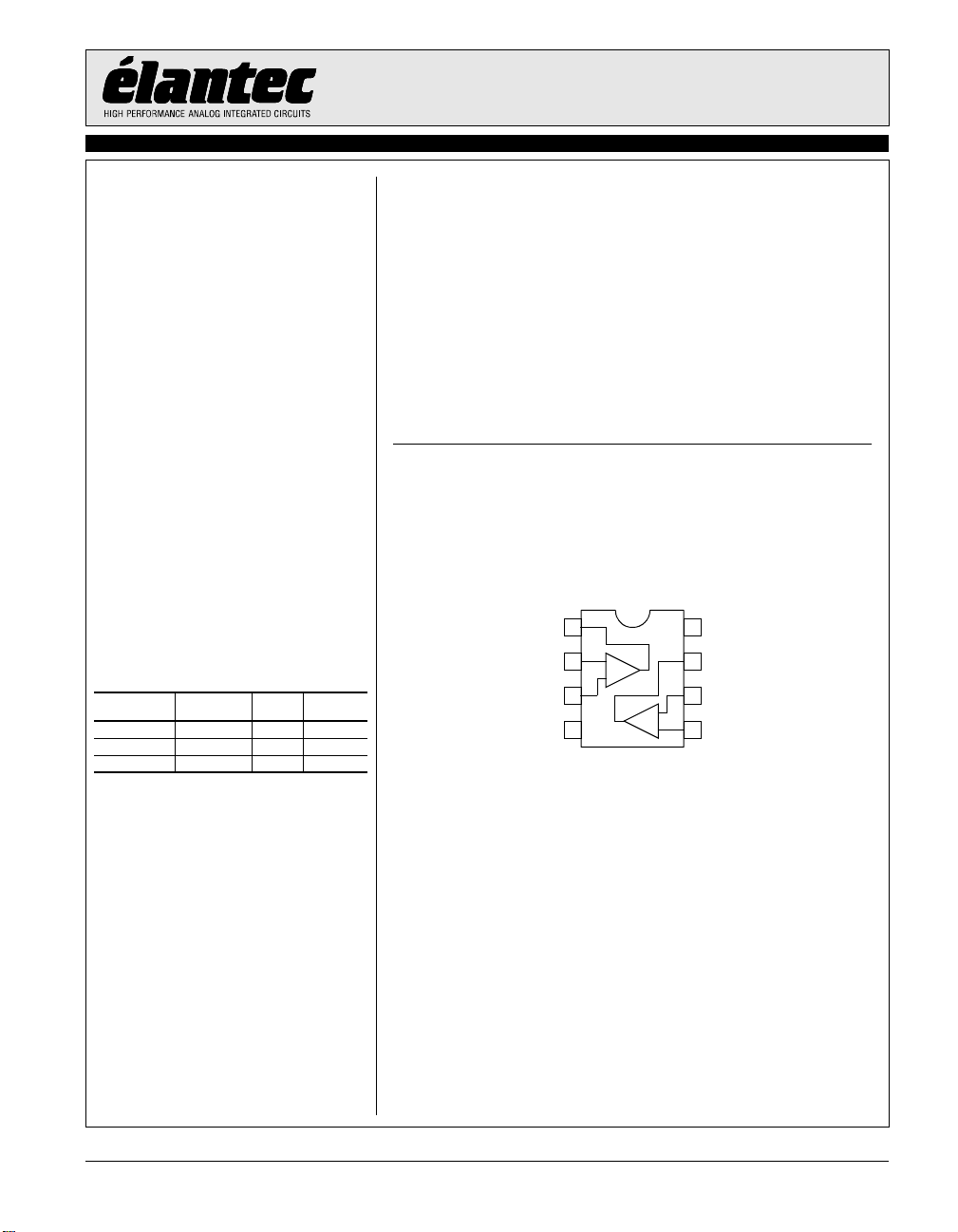
Pin Configurations
8-Pin SO
INA-
INA+
1
2
-
+
3
4
-
V
S
EL5292CS
8
VS+OUTA
7
OUTB
INB-
6
-
INB+
+
5
Note: All information contained in this data sheet has been carefully checked and is believed to be accurate as of the date of publication; however, this data sheet cannot be a “controlled document”. Current revisions, if any, to these
specifications are maintained at the factory and are available upon your request . W e recommend checking the revision level befo re finalization of your design documentation.
© 2001 Elantec Semiconductor, Inc.
April 26, 2001
EL5292C
Dual 600MHz Current Feedback Amplifier
EL5292C
Absolute Maximum Ratings (T
Values beyond absolute maximum ratings can cause the device to be prematurely damaged. Absolute maximum ratings are stress ratings only and
functional device operation is not implied.
Supply Voltage between V
Maximum Continuous Output Current 50mA
+ and VS-11V
S
= 25°C)
A
Operating Junction Temperature 125°C
Power Dissipation See Curves
Pin Voltages V
- - 0.5V to VS+ +0.5V
S
Storage Temperature -65°C to +150°C
Operating Temperature -40°C to +85°C
Important Note:
All parameters having Min/Max specifications are guaranteed. Typ values are for information purposes only. Unless otherwise noted, all tests are at the
specified temperature and are pulsed tests, therefore: T
= TC = TA.
J
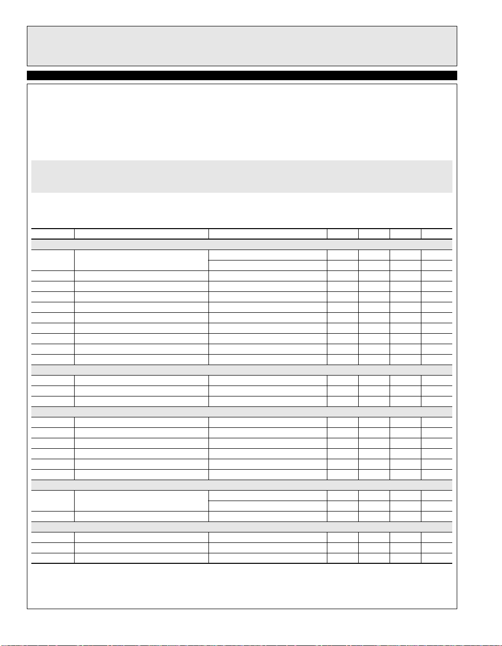
Electrical Characteristics
VS+ = +5V, VS- = -5V, RF = 750Ω for AV = 1, RF = 375Ω for AV = 2, RL = 150Ω, TA = 25°C unless otherwise specified.
Parameter Description Conditions Min Typ Max Unit
AC Performance
BW -3dB Bandwidth A
BW1 0.1dB Bandwidth 25 MHz
SR Slew Rate V
ts 0.1% Settling Time V
C
S
e
n
i
- IN- input current noise 20 pA/√Hz
n
i
+ IN+ input current noise 50 pA/√Hz
n
dG Differential Gain Error
dP Differential Phase Error
Channel Separation f = 5MHz 60 dB
Input Voltage Noise 4.1 nV/√Hz
[1]
[1]
DC Performance
V
T
R
OS
CVOS
OL
Offset Voltage -10 1 10 mV
Input Offset Voltage Temperature Coefficient Measured from T
Transimpediance 200 400 kΩ
Input Characteristics
CMIR Common Mode Input Range ±3 ±3.3 V CMRR Common Mode Rejection Ratio 42 50 dB +I
IN
-I
IN
R
IN
C
IN
+ Input Current -60 3 60 µA
- Input Current -35 4 35 µA
Input Resistance 37 kΩ
Input Capacitance 0.5 pF
Output Characteristics
V
I
OUT
O
Output Voltage Swing RL = 150Ω to GND ±3.4 ±3.7 V
Output Current RL = 10Ω to GND 95 120 mA
Supply
Is
ON
Supply Current No Load, V
PSRR Power Supply Rejection Ratio DC, V
-IPSR - Input Current Power Supply Rejection DC, V
1. Standard NTSC test, AC signal amplitude = 286mV
p-p
= +1 600 MHz
V
A
= +2 300 MHz
V
=-2.5V to +2.5V, AV = +2 2100 2300 V/µs
O
= -2.5V to +2.5V, AV = -1 9 ns
OUT
AV = +2 0.015 % AV = +2 0.04 °
to T
MIN
MAX
R
= 1KΩ to GND ±3.8 ±4.0 V
L
= 0V 5 6 7.25 mA
IN
= ±4.75V to ±5.25V 55 75 dB
S
= ±4.75 to ±5.25V -2 2 µA/V
S
5µV/°C
, f = 3.58MHz
2
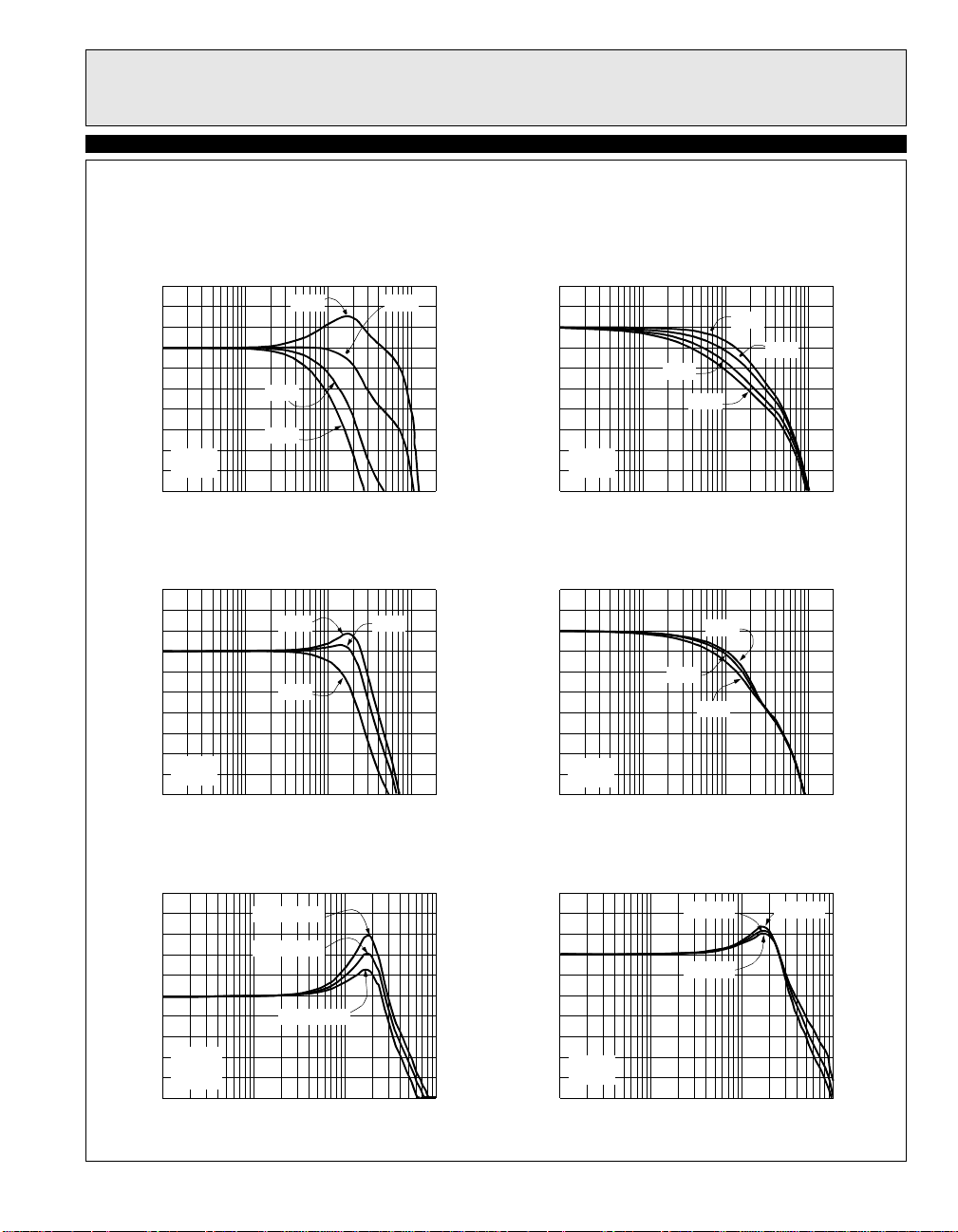
Typical Performance Curves
EL5292C
EL5292C
Dual 600MHz Current Feedback Amplifier
Non-Inverting Frequency Response (Gain)
6
2
-2
-6
Normalized Magnitude (dB)
-10
RF=750Ω
RL=150Ω
-14
1M 10M 100M 1G
Inverting Frequency Response (Gain)
6
2
-2
-6
Normalized Magnitude (dB)
-10
RF=375Ω
=150Ω
R
L
-14
1M 10M 100M 1G
AV=1
AV=5
AV=10
Frequency (Hz)
AV=-1 AV=-2
AV=-5
Frequency (Hz)
AV=2
Non-Inverting Frequency Response (Phase)
90
0
-90
Phase (°)
-180
-270
RF=750Ω
RL=150Ω
-360
1M 10M 100M 1G
Inverting Frequency Response (Phase)
90
0
-90
Phase (°)
-180
-270
RF=375Ω
=150Ω
R
L
-360
1M 10M 100M 1G
AV=5
AV=10
Frequency (Hz)
AV=-1
AV=-2
AV=-5
Frequency (Hz)
AV=1
AV=2
Frequency Response for Various CIN-
10
2pF added
6
2
-2
Normalized Magnitude (dB)
AV=2
-6
RF=375Ω
RL=150Ω
-10
1M 10M 1G
1pF added
0pF added
100M
Frequency (Hz)
Frequency Response for Various R
6
2
-2
-6
Normalized Magnitude (dB)
-10
AV=2
RF=375Ω
-14
1M 10M 100M 1G
RL=500Ω
Frequency (Hz)
L
RL=100ΩRL=150Ω
3
EL5292C
Dual 600MHz Current Feedback Amplifier
EL5292C
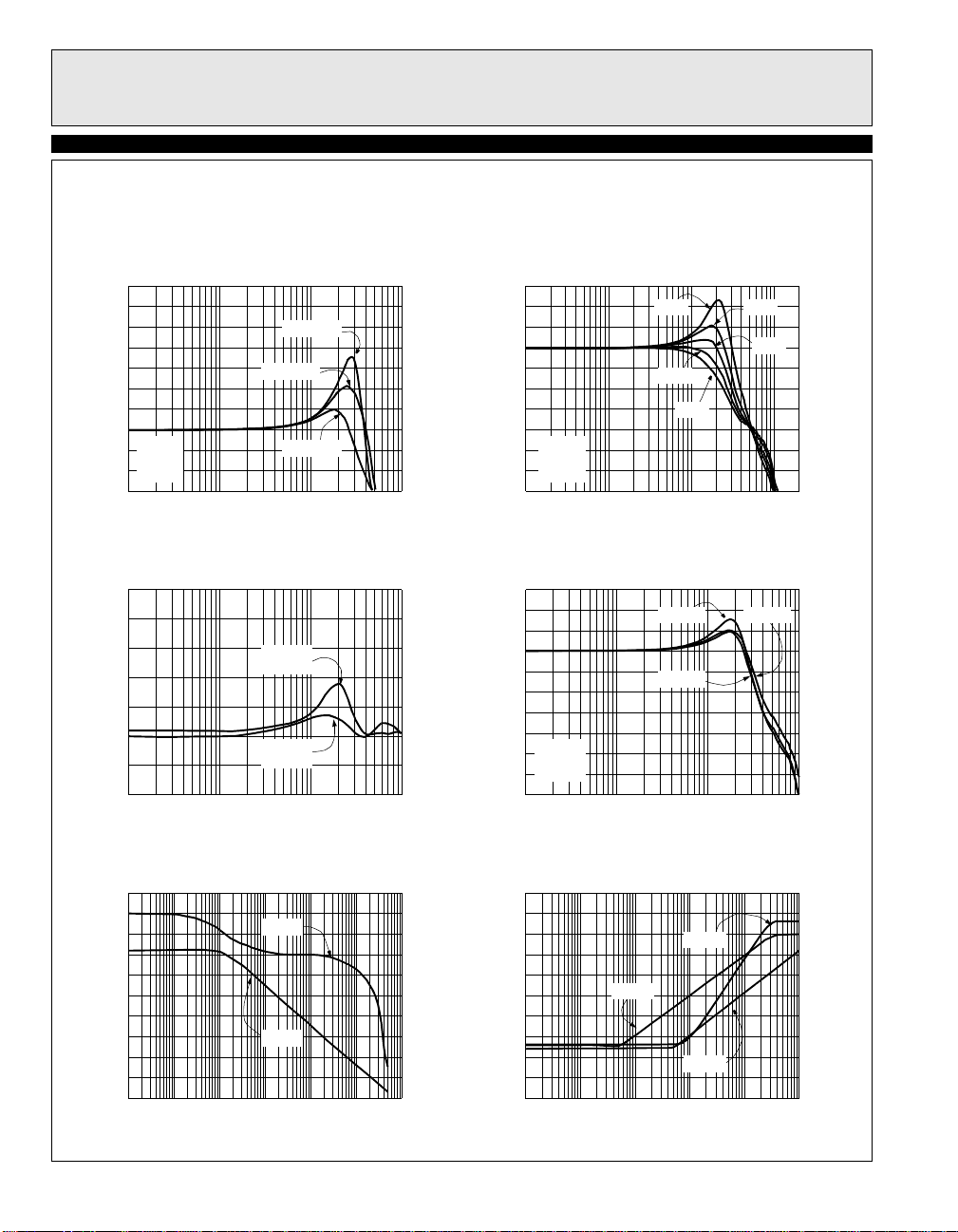
Typical Performance Curves
Frequency Response for Various C
14
10
6
2
Normalized Magnitude (dB)
AV=2
-2
RF=375Ω
RL=150Ω
-6
1M 10M 100M 1G
Frequency (Hz)
Group Delay vs Frequency
3.5
3
2.5
2
1.5
Group Delay (ns)
1
0.5
0
1M 10M 1G
Frequency (Hz)
12pF added
8pF added
0pF added
AV=2
=375Ω
R
F
AV=1
=750Ω
R
F
L
100M
Frequency Response for Various R
6
250Ω 375Ω
2
-2
-6
Normalized Magnitude (dB)
AV=2
-10
RG=R
F
RL=150Ω
-14
1M 10M 100M 1G
Frequency (Hz)
Frequency Response for Various Common-mode
Input Voltages
6
2
-2
-6
Normalized Magnitude (dB)
AV=2
-10
=375Ω
R
F
RL=150Ω
-14
1M 10M 1G
Frequency (Hz)
F
620Ω
750Ω
VCM=3V VCM=0V
VCM=-3V
100M
475Ω
Transimpedance (ROL) vs Frequency
10M
1M
)
Ω
100k
10k
Magnitude (
1k
100
1k
10k 100k 1M 10M 100M 1G
Phase
Gain
Frequency (Hz)
0
-90
-180
-270
-360
PSRR and CMRR vs Frequency
20
0
-20
Phase (°)
-40
PSRR/CMRR (dB)
-60
-80
10k
PSRR-
100k 1M 10M 1G100M
Frequency (Hz)
PSRR+
CMRR
4
Typical Performance Curves
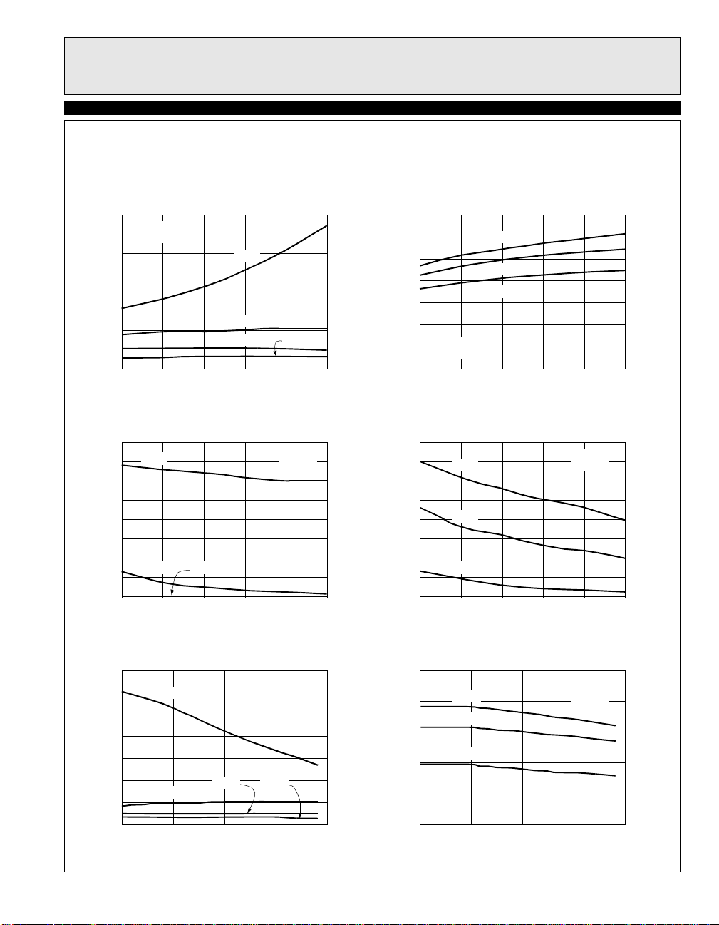
EL5292C
EL5292C
Dual 600MHz Current Feedback Amplifier
-3dB Bandwidth vs Supply Voltage for Noninverting Gains
800
RF=750Ω
RL=150Ω
600
400
-3dB Bandwidth (MHz)
200
0
567 10
Total Supply Voltage (V)
Peaking vs Supply Voltage for Non-inverting Gains
4
AV=1
3
2
Peaking (dB)
1
AV=2 AV=10
0
567 1089
Total Supply Voltage (V)
AV=1
AV=2
AV=5 AV=10
89
RF=750Ω
RL=150Ω
-3dB Bandwidth vs Supply Voltage for Inverting
Gains
350
300
250
200
150
-3dB Bandwidth (MHz)
100
RF=375Ω
50
RL=150Ω
0
567 1089
Peaking vs Supply Voltage for Inverting Gains
4
3
2
Peaking (dB)
1
0
567 1089
AV=-1
AV=-2
AV=-5
Total Supply Voltage (V)
AV=-1
AV=-2
AV=-5
Total Supply Voltage (V)
RF=375Ω
RL=150Ω
-3dB Bandwidth vs Temperature for Non-inverting
Gains
1400
1200
1000
800
600
400
-3dB Bandwidth (MHz)
200
0
AV=1
AV=2
-40 10 60 160
AV=5 AV=10
Ambient Temperature (°C)
RF=750Ω
RL=150Ω
110
-3dB Bandwidth vs Temperature for Inverting
Gains
500
400
300
200
-3dB Bandwidth (MHz)
100
0
AV=-1
AV=-2
AV=-5
-40 10 60 160
Ambient Temperature (°C)
RF=375Ω
RL=150Ω
110
5
 Loading...