ELANT EL4450CS, EL4450CN Datasheet

EL4450C
Wideband Four-Quadrant Multiplier
EL4450C
Features
• Complete four-quadrant multiplier
with output amp—requires no
extra components
• Good linearity of 0.3%
• 90 MHz bandwidth for both X and
Y inputs
• Operates on ±5V to ±15V supplies
• All inputs are differential
• 400V/µs slew rate
Applications
• Modulation/Demodulation
• RMS computation
• Real-time power computation
• Nonlinearity correction/generation
Ordering Information
Part No. Temp. Range Package Outline #
EL4450CN -40°C to +85°C 14-Pin P-DIP MDP0031 EL4450CS -40°C to +85°C 14-Lead SO MDP0027
General Description
The EL4450C is a complete four-quadrant multiplier circuit. It offers
wide bandwidth and go od line arity while incl uding a powerfu l outp ut
voltage amplifier, drawing modest supply current.
The EL4450C operates on ±5V supplies and has an analog input range
of ±2V, making it ideal for video signal processing. AC characteristics
do not vary over the ±5V t o ±15V supply range.
The multiplier has an operational temperature range of -40°C to
+85°C and are packaged in plast ic 14-pin P-DIP and SO.
© 1995 Elantec, Inc.
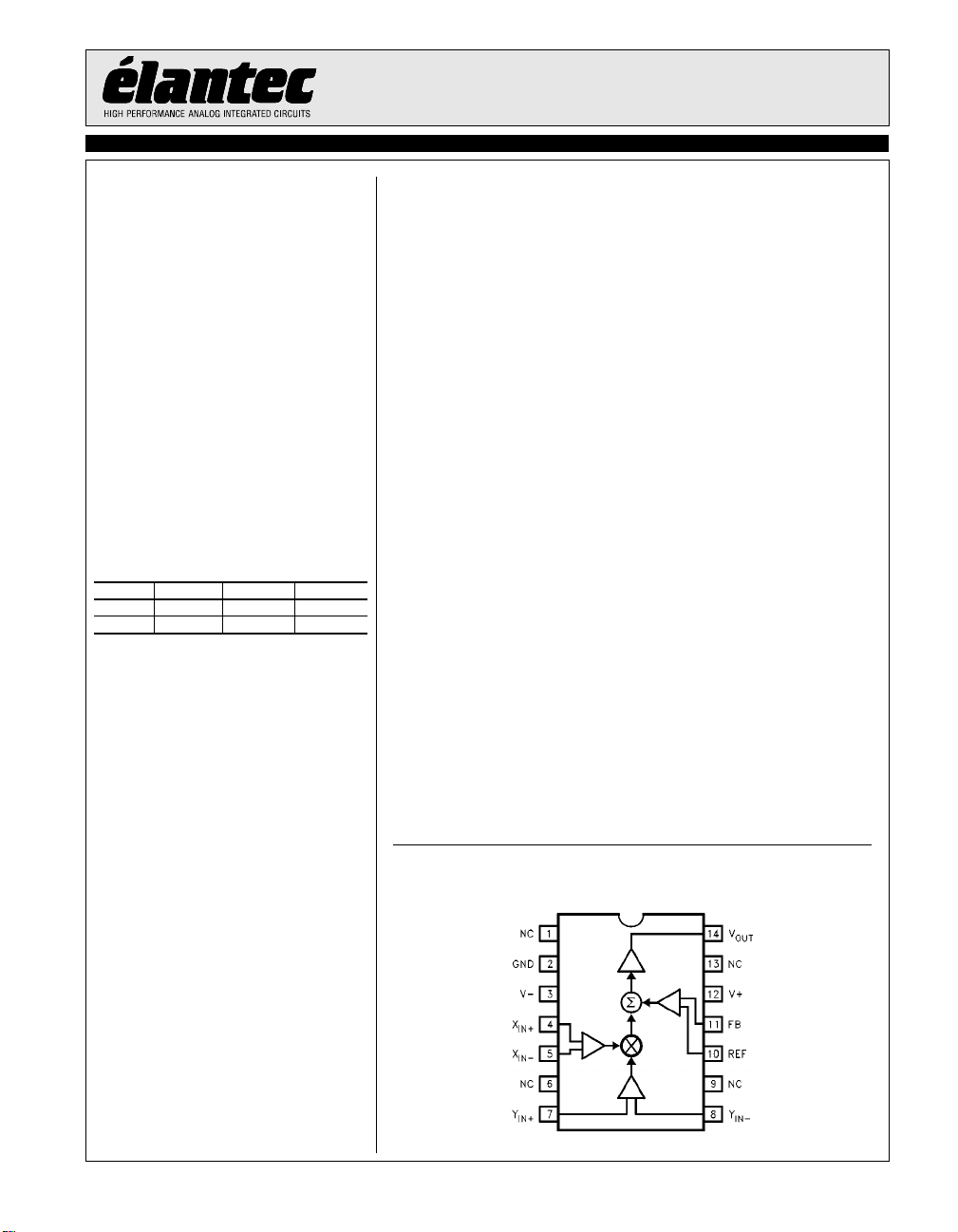
Connection Diagrams
January 1996 Rev B

EL4450C
Wideband Four-Quadrant Multiplier
EL4450C
Absolute Maximum Ratings (T
V+ Positive Supply Voltage 16.5V
V+ to V- Supply Voltage 33V
V
S
V
Voltage at any Input or Feedback V+ to V-
IN
Difference between Pairs of Inputs or Feedback 6V
V
IN
Current into any Input or Feedback Pin 4 mA
I
IN
= 25 °C)
A
Output Current 30 mA
I
OUT
Maximum Power Dissipation See Curves
P
D
T
Operating Temperature Range -40°C to +85°C
A
Storage Temperature Range -60°C to +150°C
T
S
Important Note:
All parameters having Min/Max specifications are guaranteed. The Test Level column indicates the specific device testing actually performed during
production and Quality inspection. Elantec performs most electrical tests using modern high-speed automatic test equipment, specifically the LTX77
Series system. Unless otherwise noted, all tests are pulsed tests, therefor T
= TC = TA.
J
Test Level Test Procedure
I 100% production tested and QA sample tested per QA test plan QCX0002.
II 100% production tested at T
= 25°C and QA sample tested at TA = 25°C, T
A
MAX
and T
per QA test plan QCX0002.
MIN
III QA sample tested per QA test plan QCX0002.
IV Parameter is guaranteed (but not tested) by Design and Characterization Data.
V Parameter is typical value at T
= 25°C for information purposes only.
A
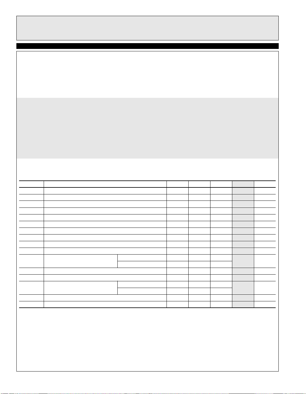
Open-Loop DC Electrical Characteristics
Power Supplies at ±5V, TA = 25°C, VFB = V
Parameter Description Min Typ Max
V
DIFF
Differential Input Voltage—Clipping 1.8 2.0 IV
0.2% nonlinearity 1.0
V
CM
V
OS
I
B
I
OS
Gain Gain Factor of V
Common-Mode Range of V
= ±15V ±12.5 ±12.8 IV
V
S
Input Offset Voltage 8 35 ImV
Input Bias Current 9 20 IµA
Input Offset Current between XIN+ and XIN-, YIN+ and YIN-, REF and FB 0.5 4 IµA
= Gain × XIN+ × Y
OUT
NLx Nonlinearity of X Input; XIN between -1V and +1V 0.3 0.7 I%
NLy Nonlinearity of Y Input; Y
R
IN
Input resistance X
CMRR Common-Mode Rejection Ratio, X
PSRR Power -Supply Rejection Ratio, FB 60 72
V
O
I
SC
I
S
Output Voltage Swing
= 0, V
(V
IN
REF
Varied)
Output Short-Circuit Current 40 85 ImA Supply Current, VS = ±15V 15.4 18 ImA
.
OUT
Test Level Units
VV
= 0, VS = ±5V ±2.5 ±2.8 IV
DIFF
IN
between -1V and +1V 0.2 0.35 I%
IN
to X
, Y
IN+
to Y
IN-
IN+
0.45 0.5 0.55 I V/V
, 230 VkΩ
IN-
2
REF to FB 90
IN
and Y
IN
70 90 IdB
IdB
V
= ±5V ± 2.5 ±2.8 IV
S
= ±15V ±12.5 ±12.8
V
S
2

Wideband Four-Quadrant Multiplier
Closed-Loop AC Electrical Characteristics
Power Supplies at ±12V, TA = 25°C, RL = 500¾, CL = 15pF
Parameter Description Min Typ Max
BW, -3 dB -3 dB Small-Signal Bandwidth, X or Y 90
BW, ±0.1 dB 0.1 dB Flatness Bandwidth 10
Peaking Frequency Response Peaking 1.0
SR Slew Rate, V
V
N
Input-Referred Noise Voltage Density 100 V nV/Hz
between -2V and +2V 300 400 I V/µs
OUT
Test Circuit
EL4450C
EL4450C
Test Level Units
V MHz
V MHz
VdB
Note: For typical performance curves, RF = 0, RG = ×, VS = ±5V, RL = 500¾, and CL = 15 pF unless otherwise noted.
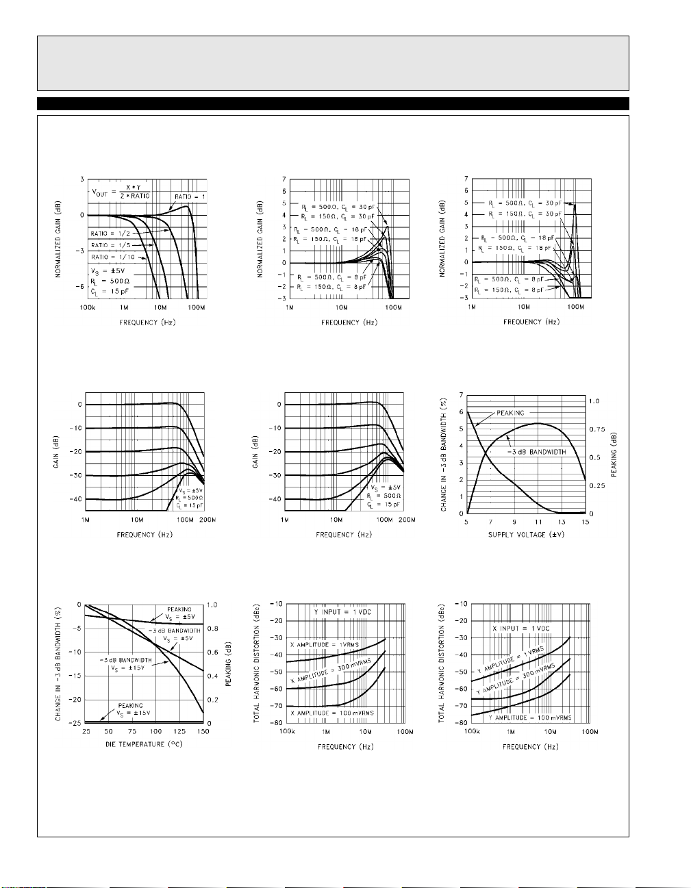
Typical Performance Curves
Transfer Function of X Input for
Various Y Inputs
Transfer Function of Y Input for
Various X Inputs
3

EL4450C
Wideband Four-Quadrant Multiplier
EL4450C
Frequency Response
for Various Feedback
Divider Ratios
X Input Frequency Response
for Various Y DC Inputs
Frequency Response
for Various RL, C
VS = ±5V
Y Input Frequency Response
for Various X DC Inputs
L
Frequency Response
for Various RL, C
VS = ±15V
-3 dB Bandwidth
and Peaking
vs Supply Voltage
L
Change in Bandwidth
and Peaking vs Temperature
Total Harmonic Distortion
of X Input vs Frequency
4
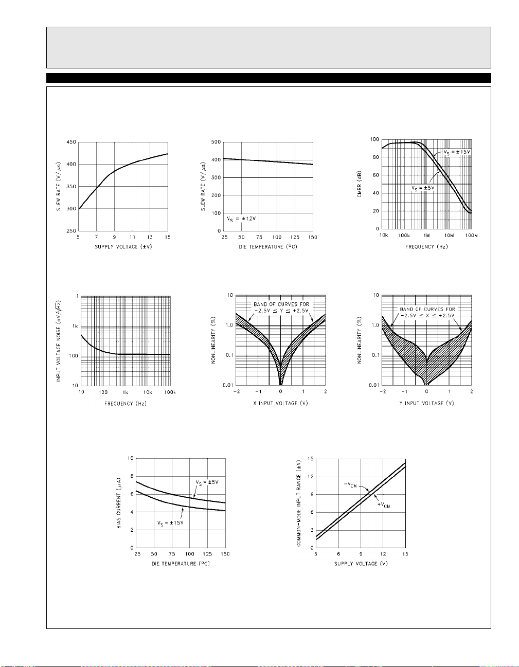
Total Harmonic Distortion
of Y Input vs Frequency

EL4450C
Wideband Four-Quadrant Multiplier
EL4450C
Slew Rate
vs Supply Voltage
Input Voltage Noise
vs Frequency
Slew Rate
vs Die Temperature
Nonlinearity of X Input
CMRR vs Frequency
Nonlinearity of Y Input
Bias Current
vs Die Temperature
Common-Mode Input Range
vs Supply Voltage
5
 Loading...