EL4332C
Triple 2:1 300 MHz Mux-Amp AV =2
EL4332C
Features
•3 ns A-B switching
• 300 MHz bandwidth
• Fixed gain of 2, for cable driving
• > 650V/µs slew rate
• TTL/CMOS compatible switch
Applications
• RGB multiplexing
• Picture-in-picture
•Cable driving
• HDTV processing
• Switched gain amplifiers
• ADC input multiplexer
Ordering Information
Part No. Temp. Range Package Outline #
EL4332CS -40°C to 85°C SO16 MDP0027
Demo Board
A demo PCB is available for this product. Request “EL4332/1 Demo Board.”
General Description
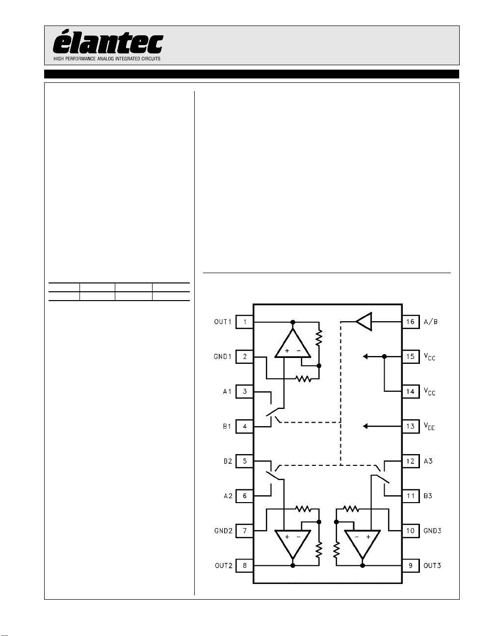
The EL4332C is a triple very h igh spee d 2:1 Mu ltip le xe r-Ampli fie r. It
is intended primarily for component video multiplexing and is especially suited for pixel switchin g. The amplifiers ha ve the ir gain set to 2
internally, which reduces the need for many external components. The
gain-of-2 facilitates driving back terminated cables. All three amplifiers are switched simultaneously from their A to B inputs by the
TTL/CMOS compatible, common A/B control pin.
A -3 dB bandwidth of 300 MHz together with 3 ns multiplexing time
enable the full performance of the fastest component video systems to
be realized.
The EL4332C runs fro m st an dard ±5V s uppl ie s, an d is a vai lable in the
narrow 16-pin small outline package.
Connection Diagrams
© 1995 Elantec, Inc.
November 12, 1999

EL4332C
Triple 2:1 300 MHz Mux-Amp AV =2
EL4332C
Absolute Maximum Ratings (T
VCC to V
EE
to any GND 12V
V
CC
to any GND 12V
V
EE
Continuous Output Current 45 mA
Any Input V
= 25 °C)
A
- 0.3V to VCC + 0.3V
EE
Input Current, Any Input 5 mA
14V
Power Dissipation See Curves
Operating Temperature -40°C to 85°C
Junction Temperature 170°C
Storage Temperature -60°C to +150°C
Important Note:
All parameters having Min/Max specifications are guaranteed. The Test Level column indicates the specific device testing actually performed during
production and Quality inspection. Elantec performs most electrical tests using modern high-speed automatic test equipment, specifically the LTX77
Series system. Unless otherwise noted, all tests are pulsed tests, therefor T
= TC = TA.
J
Test Level Test Procedure
I 100% production tested and QA sample tested per QA test plan QCX0002.
II 100% production tested at T
= 25°C and QA sample tested at TA = 25°C, T
A
MAX
and T
per QA test plan QCX0002.
MIN
III QA sample tested per QA test plan QCX0002.
IV Parameter is guaranteed (but not tested) by Design and Characterization Data.
V Parameter is typical value at T
= 25°C for information purposes only.
A
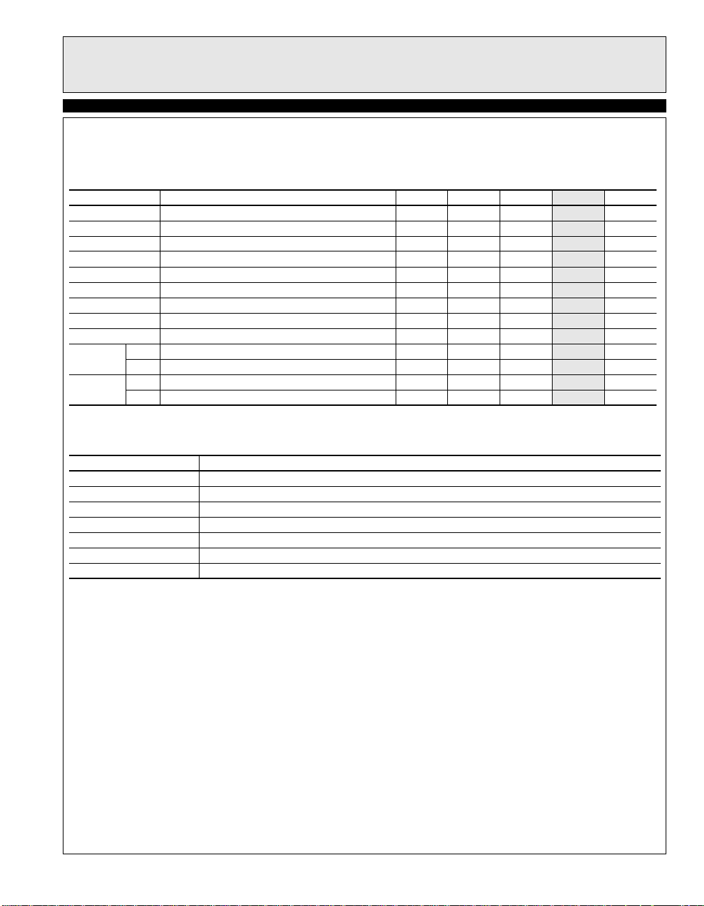
DC Electrical Characteristics
VCC = +5V, VEE = -5V, Temperature = 25°C, RL = ×
Parameter Description Min Typ Max
V
OS
dV
OS
R
IN
I
B
dI
B
A
V
dA
V
C
IN
Input Referred Offset Voltage 8 20 II mV
Input Referred Offset Voltage Delta
[1]
28II mV
Input Resistance 30 VkΩ
Input Bias Current -7 -30 II µA
Input Bias Current Delta
[1]
0.5 4.0 II µA
Gain 1.94 2.00 2.06 II V/V
[1]
Gain Delta
0.5 2.5 II %
Input Capacitance 3.3 VpF
PSRR Power Supply Rejection Ratio 50 70
V
O
Output Voltage Swing into 500Ω load ±2.7 ±3.6 II V
Output Voltage Swing into 150Ω load +3/-2.7
I
OUT
Xtalk
Xtalk
V
IH
V
IL
I
IL
I
IH
I
S
Current Output, Measured with 75W Load
Crosstalk from Non-selected Input (at DC) -70 -100 III dB
AB
Crosstalk from one Amplifier to another Amplifier -70 -100 VdB
CH-CH
Input Logic High Level 2.0 II V
Input Logic Low Level 0.8 II V
Logic Low Input Current (VIN = 0V) -0.3 -40 -80 II µA
Logic High Input Current (VIN = 0V) -3 0 3 II µA
Total Supply Current 38 48 60 II mA
[2]
30 40 II mA
1. Each channel’s A- input to its B-input.
2. There is no short circuit prot ection on any output.
Test Level Units
II dB
VV
2
EL4332C
Triple 2:1 300 MHz Mux-Amp AV =2
AC Electrical Characteristics
VCC = +5V, VEE = -5V, Temperature = 25°C, RL = 150Ω, CL = 3 pF.
Parameter Description Min Typ Max
BW -3 dB Bandwidth 300
BW 0.1dB ±0.1 dB Bandwidth 105
DG Differential Gain at 3.58 MHz 0.04
DP Differential Phase at 3.58 MHz 0.08
Pkg Peaking with Nominal Load 0.2
SR Slew Rate (4V Square Wave, Measured 25%–75%) 650
t
s
T
SW
OS Overshoot, V
ab 10M Input to Input Isolation at 10 MHz 60 VdB
I
SO
I
ch-ch 10M Channel to Channel Isolation at 10 MHz 61 VdB
SO
Settling Time to 0.1% of Final Value 13 Vns
Time to Switch Inputs 3 Vns
= 4 V
OUT
P-P
100M Input to Input Isolation at 100 MHz 40
100M Channel to Channel Isolation at 100 MHz 50
8 V%
Test Level Units
VMHz
VMHz
V%
V °
VdB
VV/µs
VdB
VdB
EL4332C
Pin Descriptions
Pin Name Function
A1, A2, A3 “A” inputs to amplifiers 1, 2 and 3 respectively
B1, B2, B3 “B” inputs to amplifiers 1, 2 and 3 respectively
GND1, GND2, GND3 These are the individual ground pins for each channel.
Out1, Out2, Out3 Amplifier outputs. Note: there is no short circuit protection on any output.
V
CC
V
EE
A/B Common input select pin, a logic high selects the “A” inputs, logic low selects the “B” inputs. CMOS/TTL compatible.
Positive power supply. Typically +5V.
Negative power supply. Typically -5V.
3
EL4332C
Triple 2:1 300 MHz Mux-Amp AV =2
EL4332C
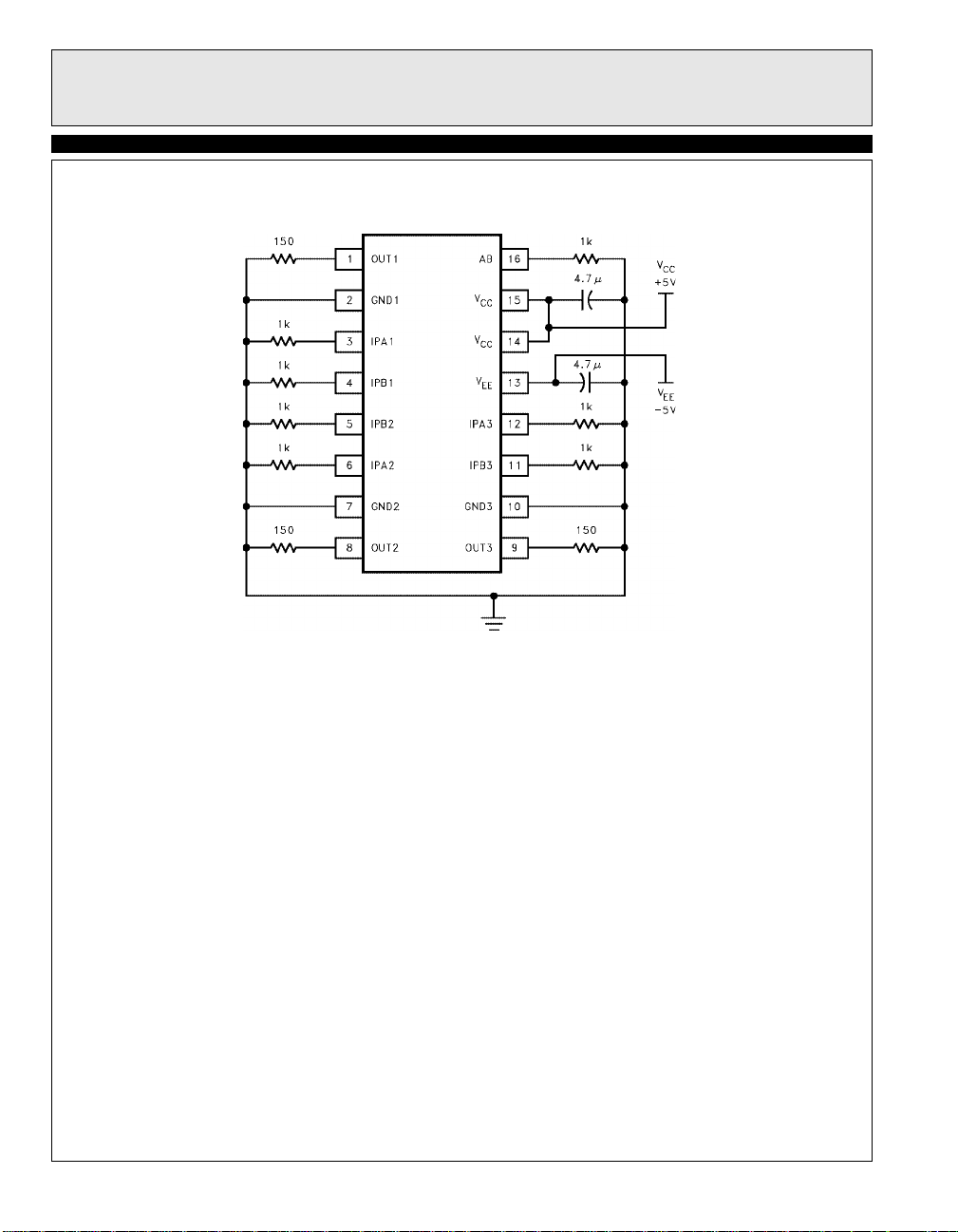
Burn In Schematic
4
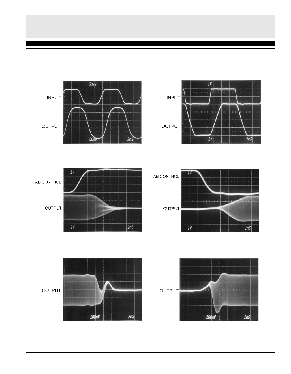
Typical Performance Curves
Small Signal Transient Response Large Signal Transient Response
EL4332C
EL4332C
Triple 2:1 300 MHz Mux-Amp AV =2
Switching to Ground from a Large
Signal Uncorrelated Sine Wave
Switching to Ground from a Small
Signal Uncorrelated Sine Wave
Switching from Ground to a Large
Signal Uncorrelated Sine Wave
Switching from Ground to a Small
Signal Uncorrelated Sine Wave
5
EL4332C
Triple 2:1 300 MHz Mux-Amp AV =2
EL4332C
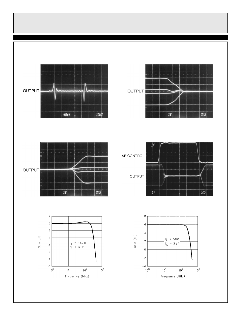
Switching Glitch
(Inputs at Ground)
Switching from Ground to a
Family of DC Levels
Switching from a Family of DC
Levels to Ground
Channel A/B Switching Delay
Gain vs Frequency Gain vs Frequency
6
 Loading...