ELANT EL4095CS, EL4095CN Datasheet
EL4095C
Video Gain Control/Fader/Multiplexer
EL4095C August 1996 Rev D
Features
# Full function video fader
# 0.02%/0.02
phase
differential gain/
§
@
100% gain
# 25 ns multiplexer included
# Output amplifier included
# Calibrated linear gain control
g
#
5V tog15V operation
# 60 MHz bandwidth
# Low thermal errors
Applications
# Video faders/wipers
# Gain control
# Graphics overlay
# Video text insertion
# Level adjust
# Modulation
Ordering Information
Part No. Temp. Range Package Outline
EL4095CNb40§Ctoa85§C 14 Pin P-DIP MDP0031
EL4095CSb40
Ctoa85§C SO-14 MDP0027
§
General Description
The EL4095C is a versatile variable-gain building block. At its
core is a fader which can variably blend two inputs together and
an output amplifier that can drive heavy loads. Each input appears as the input of a current-feedback amplifier and with external resistors can separately provide any gain desired. The
output is defined as:
e
V
OUT
A*V
(0. 5VaV
INA
GAIN
)aB*V
INB
(0.5V–V
where A and B are the fed-back gains of each channel.
Additionally, two logic inputs are provided which each override
the analog V
control and force 100% gain for one input
GAIN
and 0% for the other. The logic inputs switch in only 25 ns and
provide high attenuation to the off channel, while generating
very small glitches.
Signal bandwidth is 60 MHz, and gain-control bandwidth
20 MHz. The gain control recovers from overdrive in only
70 ns.
The EL4095C operates from
g
5V tog15V power supplies, and
is available in both 14-pin DIP and narrow surface mount packages.
Ý
Connection Diagram
14-Pin DIP, SO
GAIN
),
Top View
Manufactured under U.S. Patent No. 5,321,371, 5,374,898
Note: All information contained in this data sheet has been carefully checked and is believed to be accurate as of the date of publication; however, this data sheet cannot be a ‘‘controlled document’’. Current revisions, if any, to these
specifications are maintained at the factory and are available upon your request. We recommend checking the revision level before finalization of your design documentation.
©
1992 Elantec, Inc.
4095– 1

EL4095C
Video Gain Control/Fader/Multiplexer
Absolute Maximum Ratings
V
a
S
V
S
a
V
a
I
IN
V
GAIN
V
GAIN
Important Note:
All parameters having Min/Max specifications are guaranteed. The Test Level column indicates the specific device testing actually
performed during production and Quality inspection. Elantec performs most electrical tests using modern high-speed automatic test
equipment, specifically the LTX77 Series system. Unless otherwise noted, all tests are pulsed tests, therefore T
Test Level Test Procedure
Supply Voltage
Voltage between V
, Input Voltage (V
INA
V
INB
Current IntobV
Input Voltage V
INA
S
a
,bV
and V
INB
b
S
to (V
Input Voltage V
I 100% production tested and QA sample tested per QA test plan QCX0002.
II 100% production tested at T
III QA sample tested per QA test plan QCX0002.
IV Parameter is guaranteed (but not tested) by Design and Characterization Data.
V Parameter is typical value at T
T
MAX
and T
MIN
A
per QA test plan QCX0002.
e
(T
25§C)
A
a
18V
V
a
33V
b)b
0.3V
S
a
)a0.3V
S
5mA
g
5V
GAIN
b
to V
S
S
e
25§C and QA sample tested at T
e
25§C for information purposes only.
A
FORCE
I
OUT
T
A
T
J
T
ST
Internal Power Dissipation See Curves
a
Input Voltage
Output Current
Operating Temperature Range
b
1V toa6V
g
b
40§Ctoa85§C
35 mA
Operating Junction Temperature 0§Ctoa150§C
Storage Temperature Range
e
25§C,
A
b
65§Ctoa150§C
e
e
T
J
C
TA.
Open Loop DC Electrical Characteristics
e
g
V
S
Parameter Description
V
OS
I
a
B
I
b
B
CMRR Common Mode Rejection 65 80 I dB
b
CMRR
PSRR Power Supply Rejection Ratio 65 95 I dB
b
IPSR
R
OL
R
b
IN
V
IN
V
O
I
SC
V
IH
V
IL
I
FORCE
I
FORCE
e
15V, T
25§C, V
A
ground unless otherwise specified
GAIN
Input Offset Voltage 1.5 5 I mV
a
VINInput Bias Current 5 10 I mA
b
VINInput Bias Current 10 50 I mA
b
VINInput Bias Current
Common Mode Rejection
b
VINInput Current
Power Supply Rejection Ratio
Transimpedance 0.2 0.4 I MX
b
VINInput Resistance 80 V X
a
VINRange (Vb)a3.5 (Va)b3.5 I V
Output Voltage Swing (Vb)a2(V
Output Short-Circuit Current 80 125 160 I mA
Input High Threshold at
Force A or Force B Inputs
Input Low Threshold at
Force A or Force B Inputs
, High Input Current of Force A
or Force B, V
FORCE
, Low Input Current of Force A
or Force B, V
FORCE
Limits Test
Min Typ Max
Level
Units
0.5 1.5 I mA/V
0.2 2 I mA/V
a
b
)
2I V
2.0 I V
0.8 I V
b
e
5V
b
e
0V
440
50 I mA
b
650 I mA
TDis 0.7inTDis 4.0in
2
EL4095C
Video Gain Control/Fader/Multiplexer
Open Loop DC Electrical Characteristics
e
g
V
S
Parameter Description
Feedthrough, Feedthrough of Deselected Input to Output,
Forced Deselected Input at 100% Gain Control
V
GAIN
V
GAIN
NL, Gain Gain Control Non-linearity,
RIN, VG Impedance between V
NL, A
A
A
I
S
e
15V, T
25§C, unless otherwise specified
A
, 100% Minimum Voltage at
V
for 100% Gain
GAIN
, 0% Maximum Voltage at
V
for 0% Gain
GAIN
e
g
V
e
1 Signal Non-linearity, V
V
e
0.5 Signal Non-linearity, V
V
e
0.25 Signal Non-linearity, V
V
0.5V
IN
Supply Current 17 21 I mA
GAIN
IN
IN
IN
and V
e
e
e
g
g
g
GAIN
1V, V
1V, V
1V, V
e
0.55V
GAIN
e
0V 0.03 V %
GAIN
eb
GAIN
0.25V 0.07 0.4 I %
Closed Loop AC Electrical Characteristics
e
g
V
S
noted
Parameter Description
SR Slew Rate; V
BW Bandwidth
dG Differential Gain; AC Amplitude of 286 mV
di Differential Phase; AC Amplitude of 286 mV
T
S
T
FORCE
BW, Gain
T
REC
15V, A
V
ea
e
1, R
F
Measured at
e
R
1kX,R
IN
fromb3V toa3V
OUT
b
2V anda2V
L
e
500X,C
at 3.58 MHz on DC Offset ofb0.7V, 0V anda0.7V
at 3.58 MHz on DC Offset ofb0.7V, 0V anda0.7V
Settling Time to 0.2%; V
Propagation Delay from V
Output Signal Enabled or Disabled Amplitude
b
3 dB Gain Control Bandwidth,
Amplitude 0.5 V
V
GAIN
fromb2V toa2V
OUT
e
FORCE
P-P
, Gain Gain Control Recovery from Overload;
fromb0.7V to 0V
V
GAIN
e
15 pF, C
L
A
V
A
V
A
V
A
V
A
V
A
V
A
V
A
V
IN
b
3 dB 60 MHz
b
1 dB 30 V MHz
b
0.1 dB 6 MHz
p-p
e
100% 0.02 V %
e
50% 0.07 %
e
25% 0.07 %
p-p
e
100% 0.02 V
e
50% 0.05
e
25% 0.15
e
100% 100 V ns
e
25% 100 ns
1.4V to 50%
Ð Contd.
Limits Test
Min Typ Max
60 75 I dB
0.45 0.5 0.55 I V
b
be
2 pF, T
Min Typ Max
0.55
b
0.5
b
0.45 I V
24 I%
4.5 5.5 6.5 I kX
k
0.01 V %
e
A
25§C, A
e
100% unless otherwise
V
Limits Test
330 V V/ms
25 V ns
20 V MHz
70 V ns
Level
Level
Units
TDis 2.4inTDis 3.8in
Units
§
§
§
3
EL4095C
Video Gain Control/Fader/Multiplexer
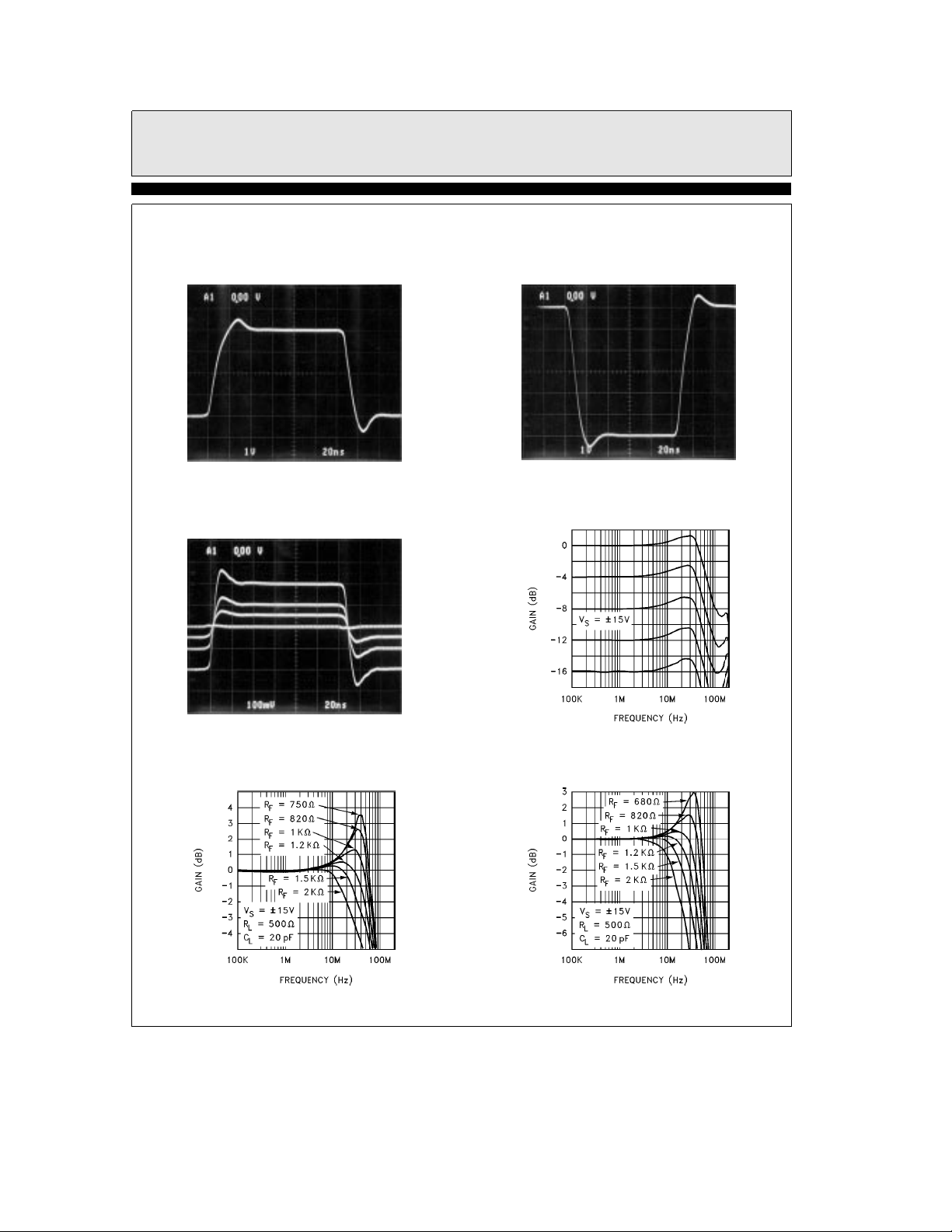
Typical Performance Curves
Large-Signal Pulse
Response Gain
ea
1
Small-Signal Pulse Response
for Various Gains
4095– 6
Large-Signal Pulse
V
ea
1
eb
1
Response Gain
Frequency Response for Different
Gains-A
4095– 7
Frequency Response with Different
Values of R
b
Gainea1
F
4095– 8
4095– 10
4095– 9
Frequency Response with Different
Values of R
b
Gaineb1
F
4095– 11
4
EL4095C
Video Gain Control/Fader/Multiplexer
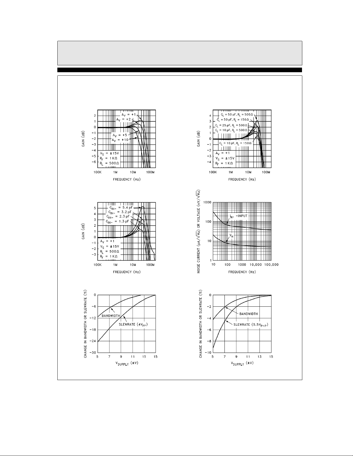
Typical Performance Curves
Frequency Response with Different Gains Load Capacitances and Resistances
Frequency Response with Various
Values of Parasitic C
b
IN
Ð Contd.
Frequency Response with Various
Input Noise Voltage and
Current vs Frequency
Change in Bandwidth and Slewrate with
Supply Voltage
b
Gainea1
Change in Bandwidth and Slewrate with
Supply VoltagebGaineb1
4095– 12
5
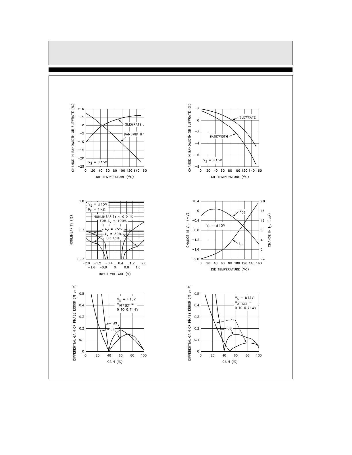
EL4095C
Video Gain Control/Fader/Multiplexer
Typical Performance Curves
Change in Bandwidth and Slewrate
with TemperaturebGainea1
DC Nonlinearity vs Input Voltage
b
Gainea1
Ð Contd.
Change in Bandwidth and Slewrate
with TemperaturebGaineb1
Change in VOSand IB- vs die Temperature
Differential Gain and Phase Errors vs
Gain Control Setting
b
Gainea1
Differential Gain and Phase Errors vs
Gain Control SettingbGaineb1
4095– 13
6
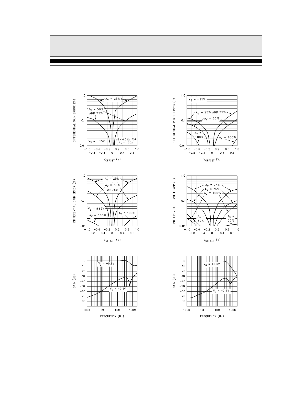
EL4095C
Video Gain Control/Fader/Multiplexer
Typical Performance Curves
Differential Phase Error vs
DC OffsetbGainea1
Differential Phase Error vs
DC Offset
b
Gaineb1
Ð Contd.
Differential Phase Error vs
DC OffsetbGainea1
Differential Phase Error vs
DC OffsetbGaineb1
Attenuation over
Frequency
b
Gainea1
Attenuation over
FrequencybGaineb1
4095– 14
7
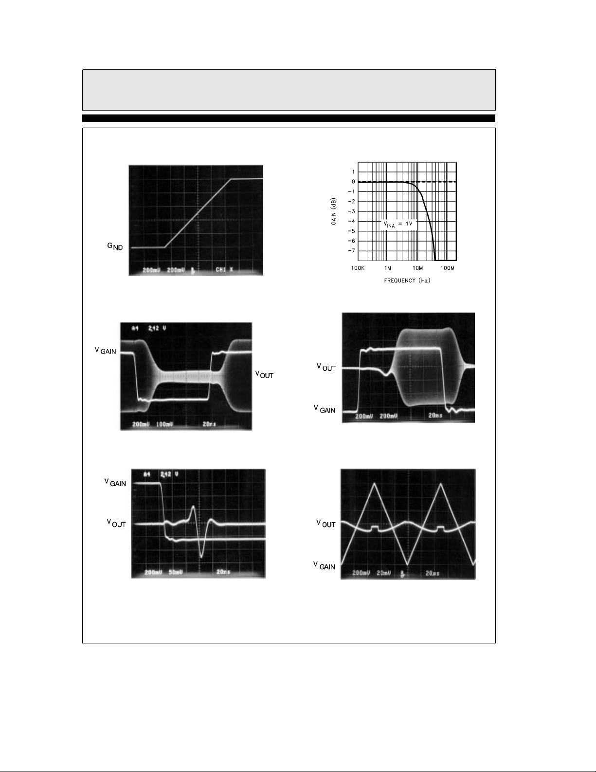
EL4095C
Video Gain Control/Fader/Multiplexer
Typical Performance Curves
Gain vs VG(1 VDCat V
Gain Control Response to a Non-Overloading
Step, Constant Sinewave at V
INA
INA
)
Ð Contd.
4095– 15
Gain Control Gain vs Frequency
V
Overload Recovery Delay
GAIN
4095– 16
V
Overload Recovery
GAIN
ResponseÐNo AC Input
4095– 17
4095– 19
4095– 18
Cross-Fade Balanceb0V on
A
and BIN; Gain
IN
8
ea
1
4095– 20
 Loading...