ELANT EL4093CS, EL4093CN Datasheet
EL4093C
300 MHz DC-Restored Video Amplifier
EL4093C January 1996 Rev B
Features
# High accuracy DC restoration for
video
# Low supply current of 9.5 mA
typ.
# 300 MHz bandwidth
# 1500V/ms slew rate
# 0.04% differential gain and 0.02
differential phase into 150X for
NTSC
# 1.5 mV max. restored DC offset
# Sample and hold amplifier with
fast enable and low leakage
# TTL-compatible HOLD logic
input
Applications
# Input amplifier in video
equipment
# Restoration amplifier in video
mixers
Ordering Information
Part No. Temp. Range Package Outline
EL4093CN -40§Ctoa85§C 16-pin P-DIP MDP0031
EL4093CS -40§Ctoa85§C 16-Lead SOIC MDP0027
General Description
The EL4093C is a complete DC-restored video amplifier subsystem, featuring low power consumption and high slew rate. It
contains a current feedback amplifier and a sample and hold
amplifier designed to stabilize video performance. When the
HOLD logic input is low, the sample and hold may be used as a
general purpose op amp to null the DC offset of the video amplifier. When the HOLD input goes high the sample and hold
§
stores the correction voltage on the hold capacitor to maintain
DC correction during the subsequent video scan line.
The sample and hold amplifier contains a current output stage
that greatly simplifies its connection to the video amplifier. Its
high output impedance also helps to preserve video linearity at
low supply voltages. For ease of interfacing, the HOLD input is
TTL-compatible. This device has an operational temperature of
b
40§Ctoa85§C and is packaged in plastic 16-pin DIP and 16-
lead SOIC.
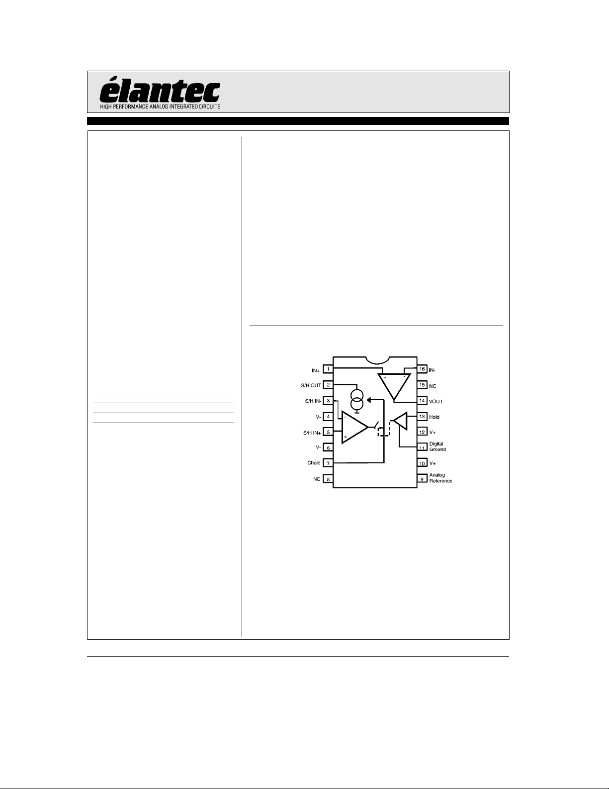
Connection Diagram
Ý
Demo Board
A demo PCB is available for this
product. Request ‘‘EL4093 Demo
Board.’’
44093– 1
Note: All information contained in this data sheet has been carefully checked and is believed to be accurate as of the date of publication; however, this data sheet cannot be a ‘‘controlled document’’. Current revisions, if any, to these
specifications are maintained at the factory and are available upon your request. We recommend checking the revision level before finalization of your design documentation.
©
1995 Elantec, Inc.
EL4093C
300 MHz DC-Restored Video Amplifier
Absolute Maximum Ratings
g
g
b
65§Ctoa150§C
e
TA.
C
Units
Units
10 mA
6mA
8V
I
S/H amplifier output current
OUT2
I
Maximum current into other pins
IN
P
Maximum Power Dissipation See Curves
D
b
T
Operating Ambient Temperature Rangeb40§Ctoa85§C
A
T
Operating Junction Temperature 150§C
J
T
Storage Temperature Range
ST
e
T
J
e
25§C,
A
Power supplies atg5V, T
e
25§C
A
Test
Level
V
Vato VbSupply Voltage 12.6V
S
V
Voltage at HOLD input
HOLD
V
Voltage at any other input Vato V
IN
DVINDifference between Sample and Hold inputs
I
Video amplifier output current
OUT1
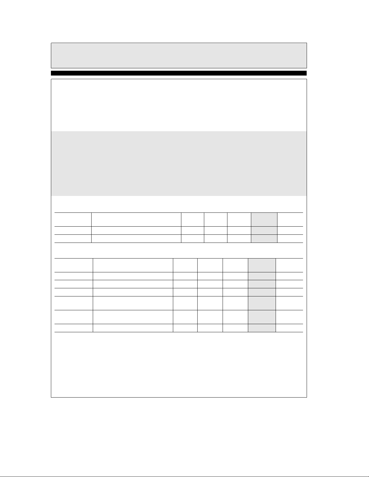
Important Note:
All parameters having Min/Max specifications are guaranteed. The Test Level column indicates the specific device testing actually
performed during production and Quality inspection. Elantec performs most electrical tests using modern high-speed automatic test
equipment, specifically the LTX77 Series system. Unless otherwise noted, all tests are pulsed tests, therefore T
Test Level Test Procedure
I 100% production tested and QA sample tested per QA test plan QCX0002.
II 100% production tested at T
III QA sample tested per QA test plan QCX0002.
IV Parameter is guaranteed (but not tested) by Design and Characterization Data.
V Parameter is typical value at T
T
MAX
and T
b
(DGND
0.7) to (DGNDa5.5V)
per QA test plan QCX0002.
MIN
g
g
30 mA
e
25§C and QA sample tested at T
A
e
25§C for information purposes only.
A
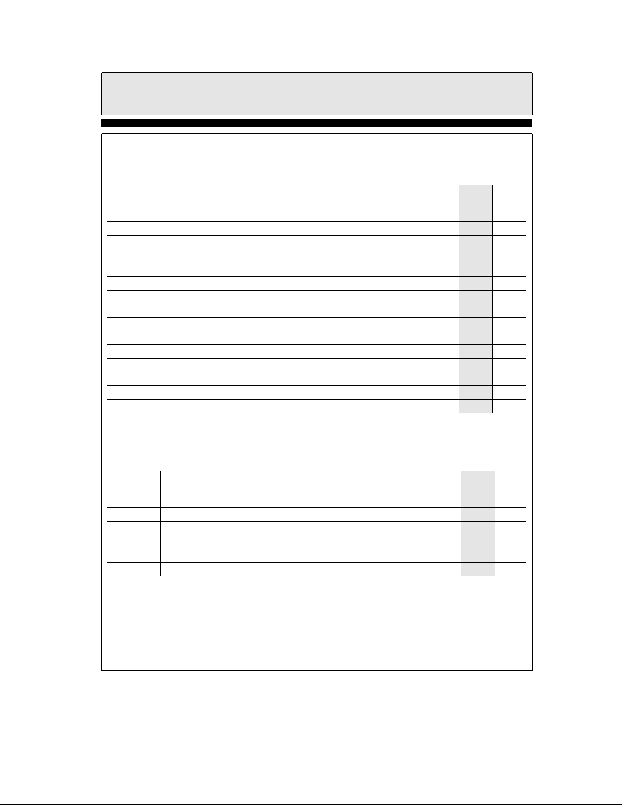
Open-Loop DC Electrical Characteristics
Parameter Description Min Typ Max
I
S,HOLD
I
S,SAMPLE
Total Supply current in HOLD mode 9.5 11.5 I mA
Total Supply current in SAMPLE mode 8.5 10.5 I mA
Video Amplifier Section (Not Restored)
Parameter Description Min Typ Max
V
OS
I
a
B
I
b
B
R
OL
V
O
I
SC
Input Offset Voltage 10 110 I mV
Non-Inverting Input Bias Current 10 25 I mA
Inverting Input Bias Current 15 50 I mA
Transimpedance
e
g
V
OUT
Output Voltage Swing
e
R
150X
L
2.5V, R
e
150X 150 400 I kX
L
g
3
g
3.5 I V
Output Short-Circuit Current 60 100 I mA
Test
Level
TABWIDE
TDis0.7in
TDis1.7in TDis1.7in
2
EL4093C
300 MHz DC-Restored Video Amplifier
Open-Loop DC Electrical Characteristics
Power supplies atg5V, T
Sample and Hold Section
Parameter Description Min Typ Max
V
OS
TCV
OS
I
B
I
OS
TCI
OS
V
CM
g
m
CMRR Common Mode Rejection Ratio (V
V
IL
V
IH
V
GND
I
DROOP
I
CHARGE
V
O
I
O
Input Offset Voltage 0.5 1.5 I mV
Average Offset Voltage Drift 6 V mV/§C
Input Bias Current 1 2 I mA
Input Offset Current 10 200 I nA
Average Offset Current Drift 0.1 V nA/§C
Common Mode Input Range
Transconductance (R
HOLD Logic Input Low (referenced to Digital GND) 0.8 I V
HOLD Logic Input High (referenced to Digital GND) 2.0 I V
Digital GND Reference Voltage (Vb)(V
Hold Mode Droop Current 10 70 I nA
Charge Current Available to C
Output Voltage Swing (R
Output Current Swing (R
e
25§C Ð Contd.
A
g
g
2.5
2.8 I V
e
500X) 5 15 I A/V
L
b
2.5V toa2.5V) 70 90 I dB
CM
g
g
5.5
HOLD
e
10kX)
L
e
0X)
L
g
g
8.5 I mA
g
3
3.5 I V
g
4.5
5.5 I mA
Closed-Loop AC Electrical Characteristics
Power supplies atg5V, T
e
25§C, R
A
e
e
R
G
750X,R
F
L
e
150X,C
e
5 pF, C
L
(parasitic)e1.8 pF
b
IN
a
b
)
4.0 I V
Test
Level
Units
Video Amplifier Section
Parameter Description Min Typ Max
BW,b3dB
b
3 dB Small-Signal Bandwidth 300 V MHz
BW,g0.1 dB 0.1 dB Flatness Bandwidth 50 V MHz
Peaking Frequency Response Peaking 0 V dB
SR Slew rate, V
betweenb2V anda2V 1500 V V/ms
OUT
dG Differential Gain Error, Voffset betweenb714 mV anda714 mV 0.04 V %
di Differential Phase Error, Voffset betweenb714 mV anda714 mV 0.02 V
3
Test
Levels
Units
§
TDis1.5in TDis1.5in
EL4093C
300 MHz DC-Restored Video Amplifier
Closed-Loop AC Electrical Characteristics
Power supplies atg5V, T
e
25§C, R
A
Sample and Hold Section
Parameter Description Min Typ Max
DI
DT
DT
T
STEP
SH
HS
AC
Change in Sample to Hold Output Current Due to Hold Step 0.1 V mA
Sample to Hold Delay Time 15 V ns
Hold to Sample Delay Time 40 V ns
Settling Time to 1% (DC Restored Amplifier Output) 2.2 V ms
Video Amplifier Input from 0 to 1V
e
e
R
G
750X,R
F
L
e
150X,C
e
5 pF, C
L
HOLD
e
2.2 nF
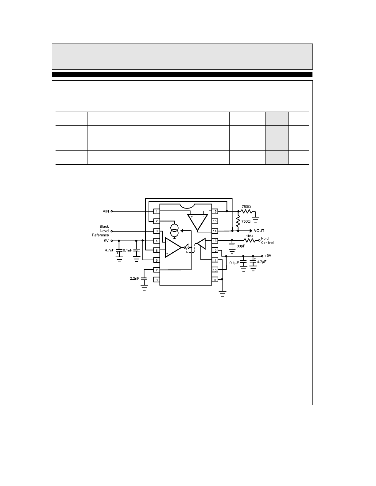
Typical Application
Test
Levels
Units
TDis1.2in
44093– 2
4
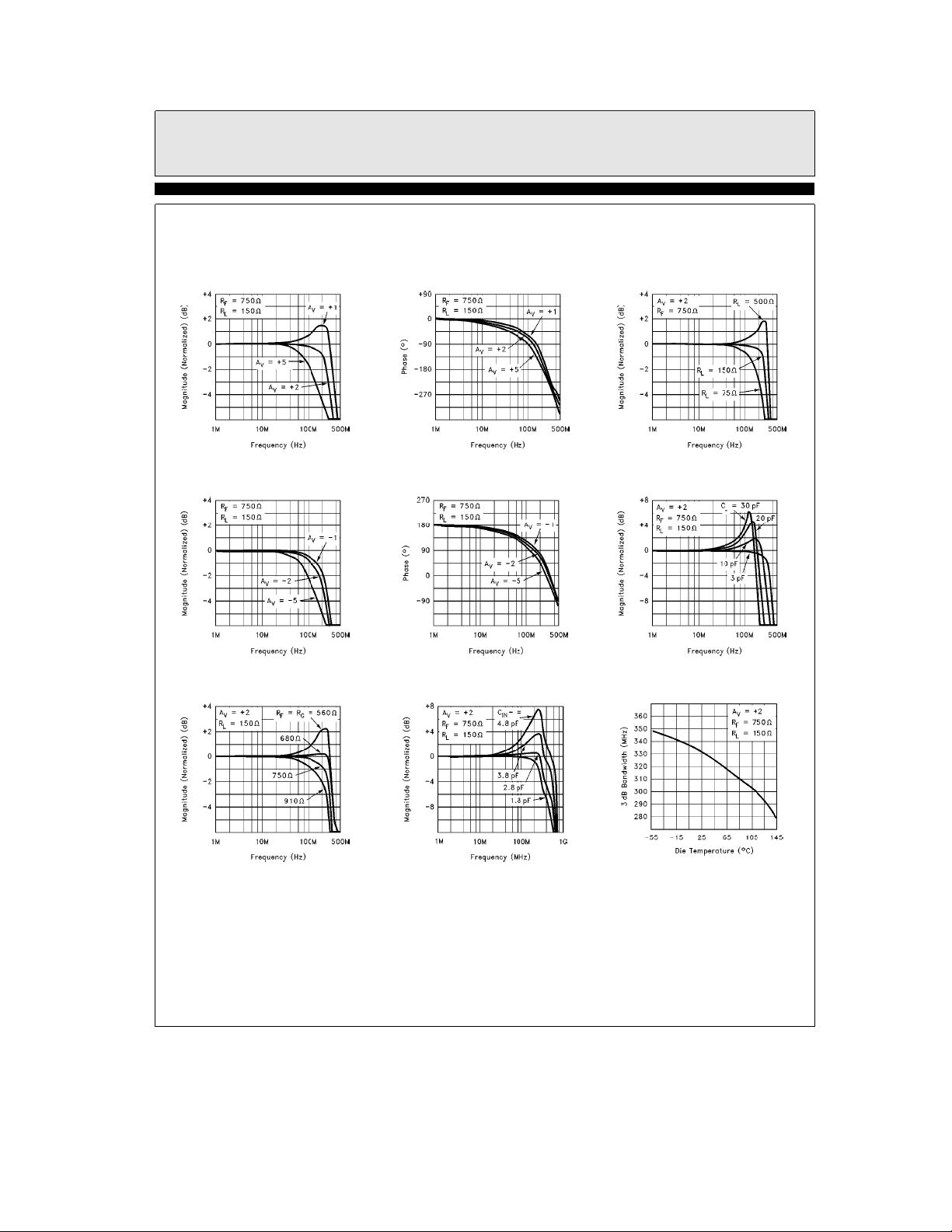
Typical Performance Curves
EL4093C
300 MHz DC-Restored Video Amplifier
Non-inverting Frequency
Response (Gain)
Inverting Frequency
Response (Gain)
Frequency Response for
Various RFand R
G
44093– 4
44093– 7
Non-inverting Frequency
Response (Phase)
Inverting Frequency
Response (Phase)
Frequency Response
for Various C
IN
44093– 5
44093– 8
Frequency Response
for Various R
Frequency Response
for Various C
3 dB Bandwidth vs
Temperature (Video Amp)
L
L
44093– 6
44093– 9
44093– 10
44093– 11
44093– 12
5
 Loading...