ELANT EL2120CS, EL2120CN Datasheet

EL2120C
100 MHz Current Feedback Amplifier
EL2120C January 1996 Rev E
Features
# Excellent differential gain and
phase on
# 100 MHz
gains of
# 700 V/ms slew rate
# 0.1 dB flatness to 20 MHz
# Output disable in 50 ns - remains
high impedance even when
driven with large slew rates
# Single
# AC characteristics are lot and
temperature stable
# Available in small SO-8 package
g
5V tog15V supplies
b
3 dB bandwidth from
g
1tog10
a
5V supply operation
Applications
# Video gain block
# Residue amplifier
# Multiplexer
# Current to voltage converter
# Coax cable driver with gain of 2
# ADC driver
Ordering Information
Part No. Temp. Range Package Outline
EL2120CN 0§Ctoa75§C 8-Pin P-DIP MDP0031
EL2120CS 0§Ctoa75§C 8-Lead SO MDP0027
General Description
The EL2120C is a wideband current feedback amplifier optimized for video performance. Its 0.01% differential gain and
0.03 degree differential phase performance when at
plies exceeds the performance of other amplifiers running on
g
15V supplies. Operating ong8tog15V supplies reduces distortions to 0.01% and 0.01 degrees and below. The EL2120C can
operate with supplies as low as
g
2.5V or a singlea5V supply.
Being a current feedback design, bandwidth is a relatively constant 100 MHz over the
g
1tog10 gain range. The EL2120C
has been optimized for flat gain over frequency and all characteristics are maintained at positive unity gain. Because the input slew rate is similar to the 700 V/ms output slew rate the
part makes an excellent high-speed buffer.
The EL2120C has a superior output disable function. Time to
enable or disable is 50 ns and does not change markedly with
temperature. Furthermore, in disable mode the output does not
draw excessive currents when driven with 1000 V/ms slew rates.
The output appears asa3pFload when disabled.
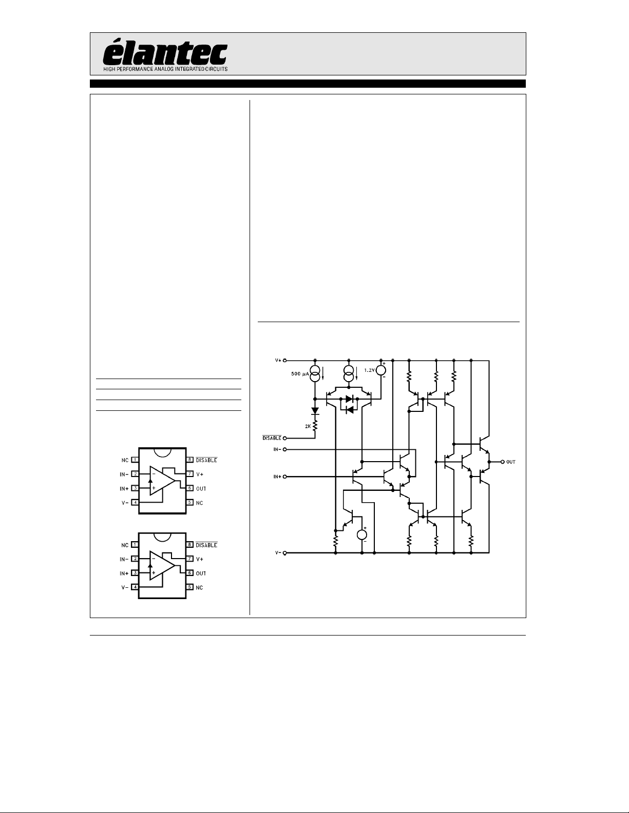
Simplified Schematic
Ý
g
5V sup-
Connection Diagrams
P-DIP
2120– 1
SO
2120– 21
Top View
Note: All information contained in this data sheet has been carefully checked and is believed to be accurate as of the date of publication; however, this data sheet cannot be a ‘‘controlled document’’. Current revisions, if any, to these
specifications are maintained at the factory and are available upon your request. We recommend checking the revision level before finalization of your design documentation.
©
1991 Elantec, Inc.
2120– 2

EL2120C
100 MHz Current Feedback Amplifier
Absolute Maximum Ratings
a
Voltage between V
a
Voltage at
b
Voltage between
a
IN,
IN, V
OUT
IN andbIN
Voltage at /Disable (V
a
Current into
b
IN, and /Disable
Important Note:
All parameters having Min/Max specifications are guaranteed. The Test Level column indicates the specific device testing actually
performed during production and Quality inspection. Elantec performs most electrical tests using modern high-speed automatic test
equipment, specifically the LTX77 Series system. Unless otherwise noted, all tests are pulsed tests, therefore T
Test Level Test Procedure
IN,
I 100% production tested and QA sample tested per QA test plan QCX0002.
II 100% production tested at T
III QA sample tested per QA test plan QCX0002.
IV Parameter is guaranteed (but not tested) by Design and Characterization Data.
V Parameter is typical value at T
and V
T
MAX
b
(Vb)b0.5V to (Va)a0.5V
a)b
10V to (Va)a0.5V
and T
MIN
A
per QA test plan QCX0002.
e
(T
25§C)
A
Output Current
33V
Internal Power Dissipation See Curves
Operating Ambient
Temperature Range 0
g
5V
Operating Junction Temperature
P-DIP or SO 150
Storage Temperature Range
g
5mA
e
25§C and QA sample tested at T
e
25§C for information purposes only.
A
g
50 mA
to 75§C
§
b
65§Ctoa150§C
e
e
T
TA.
J
C
e
25§C,
A
§
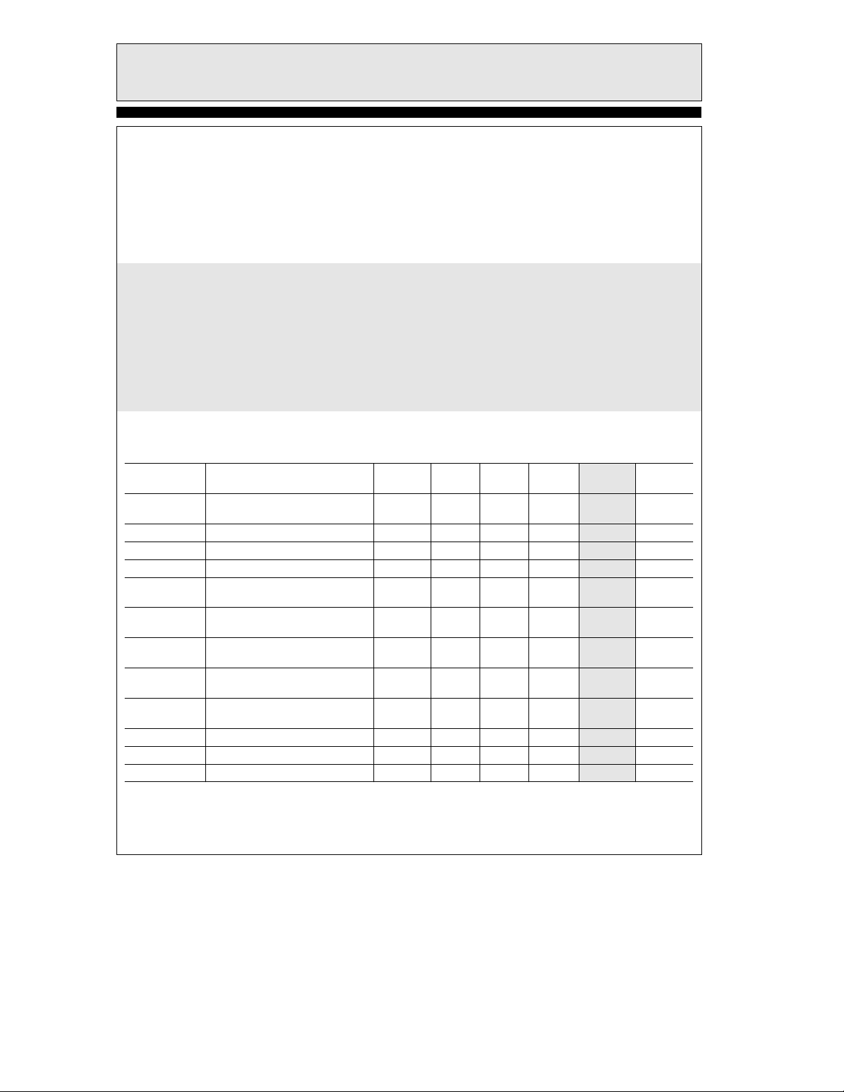
Open Loop DC Electrical Characteristics
e
g
V
S
Parameter Description Temp Min Typ Max
V
OS
DVOS/DT Input Offset Drift Full 20 V mV/§C
I
a
B
I
b
B
CMRR Common-Mode Rejection
b
ICMR
PSRR Power Supply Rejection
a
IPSR
b
IPSR
R
OL
A
VOL
a
R
5V; R
IN
L
e
150X,T
e
25§C unless otherwise specified
A
Input Offset Voltage Full 4 20 II mV
e
g
15V Full 2 25 II mV
V
S
a
VINInput Bias Current Full 5 15 II mA
b
VINInput Bias Current Full 10 50 II mA
(Note 1)
b
Input Current Common-Mode
Rejection (Note 1)
(Note 2)
a
Input Current Power Supply
Rejection (Note 2)
b
Input Current Power Supply
Rejection (Note 2)
Full 50 55 II dB
Full 8 20 II mA/V
Full 65 80 II dB
C 0.03 V mA/V
25
§
Full 0.6 5 II mA/V
Transimpedance Full 70 140 II kX
Voltage Gain Full 58 66 II dB
a
VINInput Impedance 25§C2 VMX
Test
Level
Units
C
TDis 3.2in
2

EL2120C
100 MHz Current Feedback Amplifier
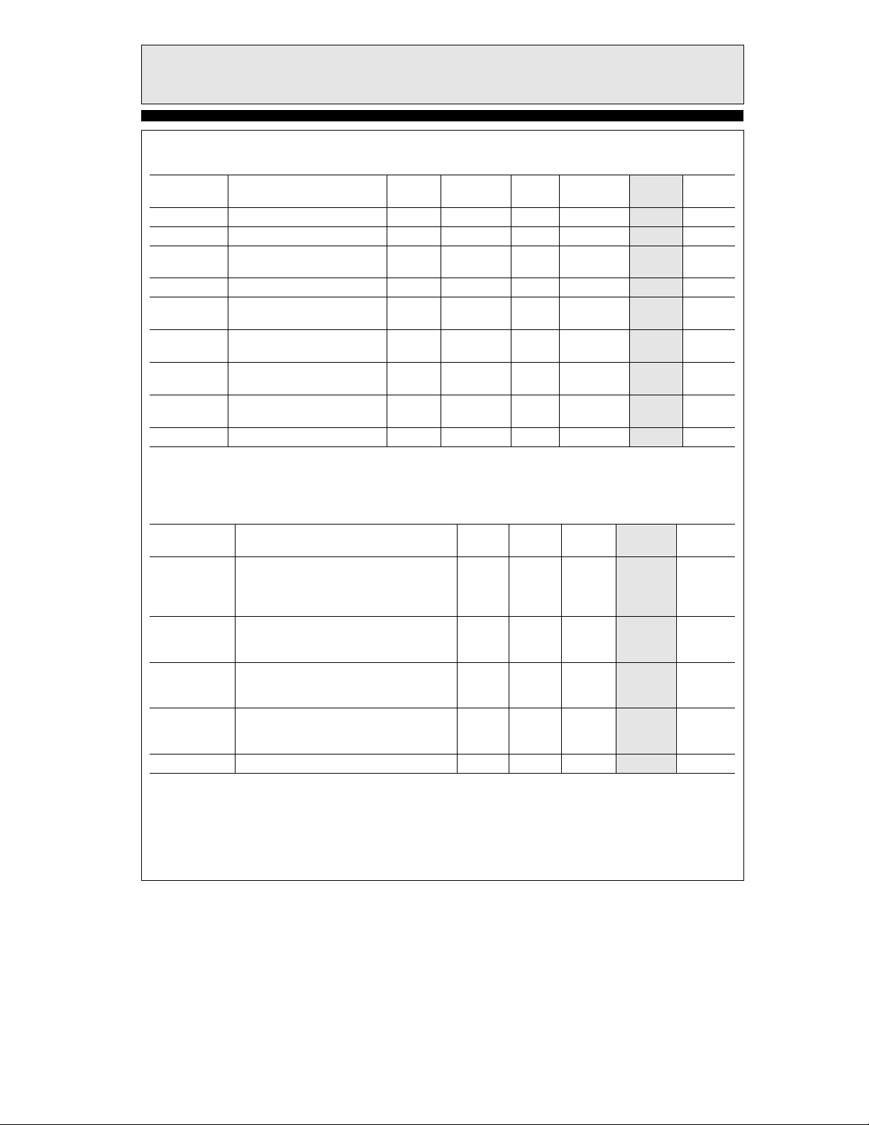
Open Loop DC Electrical Characteristics
e
V
S
Parameter Description Temp Min Typ Max
V
IN
V
O
I
SC
I
O,DIS
V
DIS,ON
V
DIS,OFF
I
DIS,ON
I
DIS,OFF
I
S
g
5V; R
L
e
150X,T
e
25§C unless otherwise specified
A
a
VINRange Full
Output Voltage Swing Full
Output Short-Circuit
Current
25
C 100 II mA
§
Output Current, Disabled Full 5 50 II mA
Disable Pin Voltage for
Output Enabled
Disable Pin Voltage for
Output Disabled
Disable Pin Current for
Output Enabled
Disable Pin Current for
Output Disabled
Supply Current (V
e
S
g
15V) Full 17 20 II mA
Full (V
Full (V
Full 5 II mA
Full 1.0 II mA
Ð Contd.
Test
Level
g
3.0
g
3.0
a)b
g
3.5 II V
g
3.5 II V
1IIV
a)b
4II V
Note 1: The input is moved fromb3V toa3V.
g
Note 2: The supplies are moved from
5V tog15V.
Closed Loop AC Electrical Characteristics
e
g
V
S
Parameter Description Min Typ Max
SR Slew Rate; V
t
S
BW Bandwidth
BW@2.5V Bandwidth at
Peaking 0.5 V dB
15V; A
V
ea
2(R
e
R
F
Measured at
Settling Time to 0.25% of a
a
0to
10V Swing; A
e
R
270X,R
F
e
g
V
2.5V
S
e
270X); R
G
fromb3V toa3V
OUT
b
2V anda2V
e %
G
ea
V
, and R
L
e
150X;C
e
7 pF; C
L
e
g
V
15V 750 V V/ms
S
e
g
V
5V 550 V V/ms
S
e
b
IN
2 pF; T
e
25§C
A
1 with
e
400X 50 V ns
L
b
3 dB 95 V MHz
g
1 dB 50 V MHz
g
0.1 dB 16 V MHz
b
3 dB 75 V MHz
g
1 dB 35 V MHz
g
0.1 dB 11 V MHz
Test
Level
Units
TDis 2.7inTDis 2.4in
Units
3

EL2120C
100 MHz Current Feedback Amplifier
Closed Loop AC Electrical Characteristics
e
g
V
S
15V; A
V
ea
2(R
e
e
R
G
270X); R
F
L
e
150X;C
e
7 pF; C
L
b
IN
Ð Contd.
e
2 pF; T
e
25§C
A
Parameter Description Min Typ Max
dG Differential Gain; DC Offset
b
from
0.7V througha0.7V, AC
Amplitude 286 mVp –p
e
g
V
15V, fe3.58 MHz
S
e
g
V
15V, fe30 MHz 0.1 V %
S
e
g
V
5V, fe3.58 MHz 0.01 V %
S
k
0.01 V %
di Differential Phase; DC Offset
b
from
0.7V througha0.7V, AC
Amplitude 286 mVp –p
e
g
V
15V, fe3.58 MHz 0.01 V
S
e
g
V
15V, fe30 MHz 0.1 V
S
e
g
V
5V, fe3.58 MHz 0.06 V
S
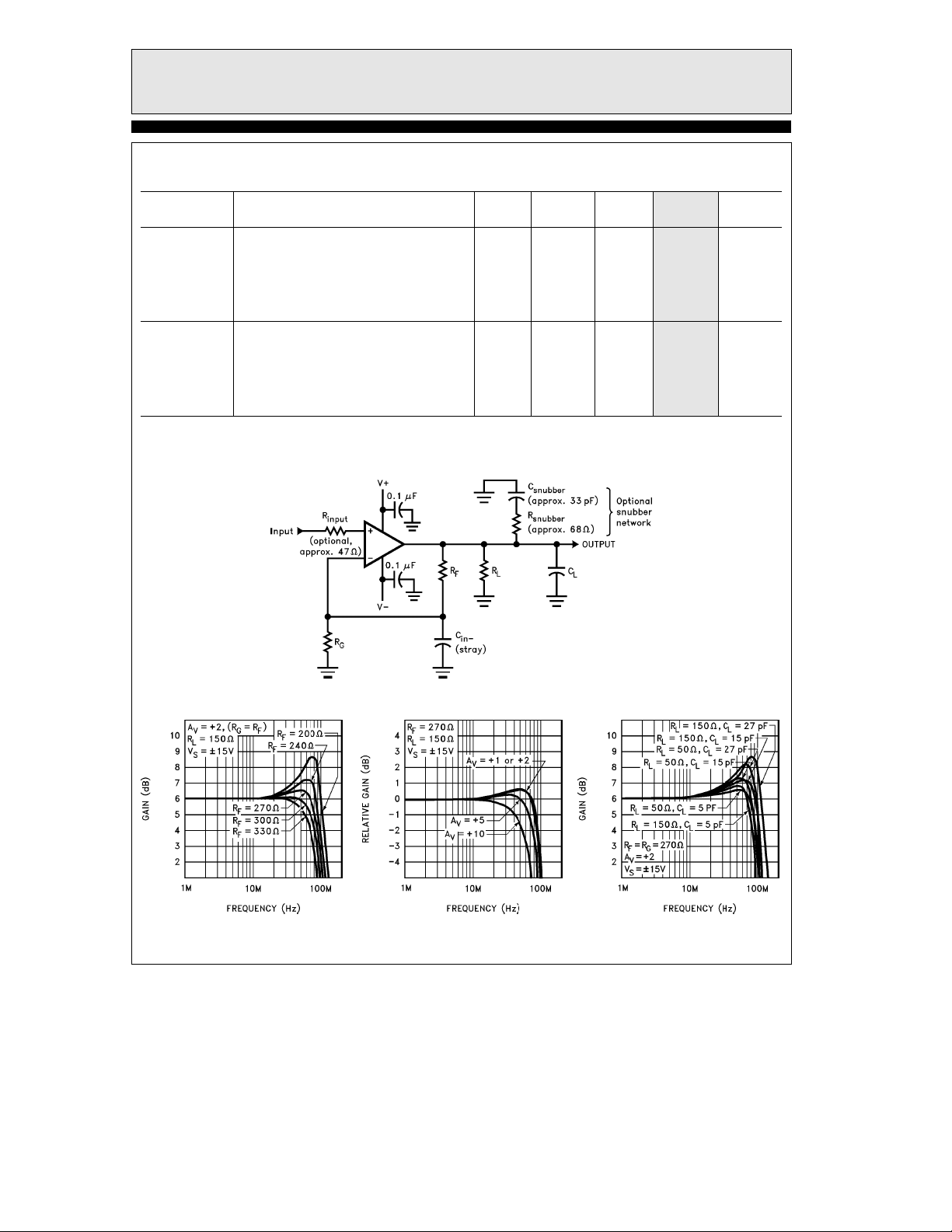
Typical Performance Curves
AC Test Circuit
Test
Level
Units
§
§
§
TDis 2.0in
Frequency Response vs R
F
2120– 4
Frequency Response vs Gain
2120– 5
4
2120– 3
Frequency Response vs Load
2120– 6
 Loading...