EL2090C
100 MHz DC-Restored Video Amplifier
EL2090C January 1996 Rev D
Features
# Complete video level restoration
system
# 0.01% differential gain and 0.02
differential phase accuracy at
NTSC
# 100 MHz bandwidth
# 0.1 dB flatness to 20 MHz
# Sample-and-hold has 15 nA
typical leakage and 1.5 pC charge
injection
# System can acquire DC
correction level in 10 ms, or 5 scan
lines of 2 ms each, to (/2 IRE
e
S
g
5V tog15V
# V
# TTL/CMOS hold signal
Applications
# Input amplifier in video
equipment
# Restoration amplifier in video
mixers
Ordering Information
Part No. Temp. Range Pkg. Outline
EL2090CN 0§Ctoa75§C 14-Pin P-DIP MDP0031
EL2090CM 0§Ctoa75§C 16-Lead SOL MDP0027
General Description
The EL2090C is the first complete DC-restored monolithic video amplifier sub-system. It contains a very high-quality video
amplifier and a nulling sample-and-hold amplifier specifically
§
designed to stabilize video performance. When the HOLD logic
input is set to a logic 0 during a horizontal sync, the sampleand-hold amplifier may be used as a general-purpose op-amp to
null the DC offset of the video amplifier. When the HOLD input goes to a logic 1 the sample-and-hold stores the correction
voltage on the hold capacitor to maintain DC correction during
the subsequent scan line.
The video amplifier is optimized for video characteristics, and
performance at NTSC is nearly perfect. It is a current-feedback
amplifier, so that
closed-loop gains. The amplifier easily drives video signal levels
into 75X loads. With 100 MHz bandwidth, the EL2090 is also
useful in HDTV applications.
The sample-and-hold is optimized for fast sync pulse response.
The application circuit shown will restore the video DC level in
five scan lines, even if the HOLD pulse is only 2 ms long. The
output impedance of the sample-and-hold is low and constant
over frequency and load current so that the performance of the
video amplifier is not compromised by connections to the DC
restore circuitry.
Ý
The EL2090C is fabricated in Elantec’s proprietary Complementary Bipolar process which produces NPN and PNP transistors with equivalent AC and DC performance. The EL2090C
is specified for operation over the 0
range.
b
3 dB bandwidth changes little at various
Cto75§C temperature
§
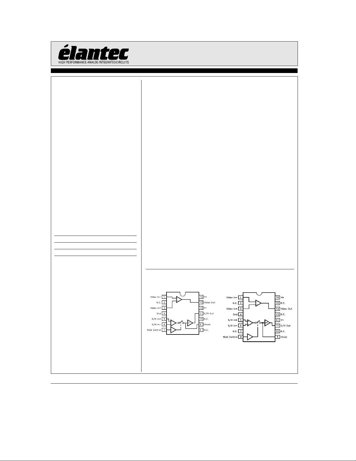
Connection Diagrams
14-Pin DIP Package 16-Pin SOL Package
2090– 1
2090– 2
Note: All information contained in this data sheet has been carefully checked and is believed to be accurate as of the date of publication; however, this data sheet cannot be a ‘‘controlled document’’. Current revisions, if any, to these
specifications are maintained at the factory and are available upon your request. We recommend checking the revision level before finalization of your design documentation. Patent pending.
©
1990 Elantec, Inc.
CMSÝ2090DS

EL2090C
100 MHz DC-Restored Video Amplifier
Absolute Maximum Ratings
a
Voltage between V
Voltage between V
V
Current into V
Important Note:
All parameters having Min/Max specifications are guaranteed. The Test Level column indicates the specific device testing actually
performed during production and Quality inspection. Elantec performs most electrical tests using modern high-speed automatic test
equipment, specifically the LTX77 Series system. Unless otherwise noted, all tests are pulsed tests, therefore T
Test Level Test Procedure
,C
S/H
b
IN
HOLD
Current 60 mA
OUT
b
IN
I 100% production tested and QA sample tested per QA test plan QCX0002.
II 100% production tested at T
III QA sample tested per QA test plan QCX0002.
IV Parameter is guaranteed (but not tested) by Design and Characterization Data.
V Parameter is typical value at T
b
and V
, S/H
a
IN
, and GND pins (Va)a0.5V
,
a
IN
and HOLD Pins 5 mA
T
MAX
and T
MIN
A
per QA test plan QCX0002.
e
(T
25§C)
A
36V
Current S/H
Internal Power Dissipation See Curves
to (V
b)b
0.5V
Operating Ambient Temperature Range 0
Operating Junction Temperature
Plastic DIP or SOL 150
Storage Temperature Range
e
25§C and QA sample tested at T
e
25§C for information purposes only.
A
OUT
b
e
T
J
C
e
25§C,
A
16 mA
Cto75§C
§
65§Ctoa150§C
e
TA.
§
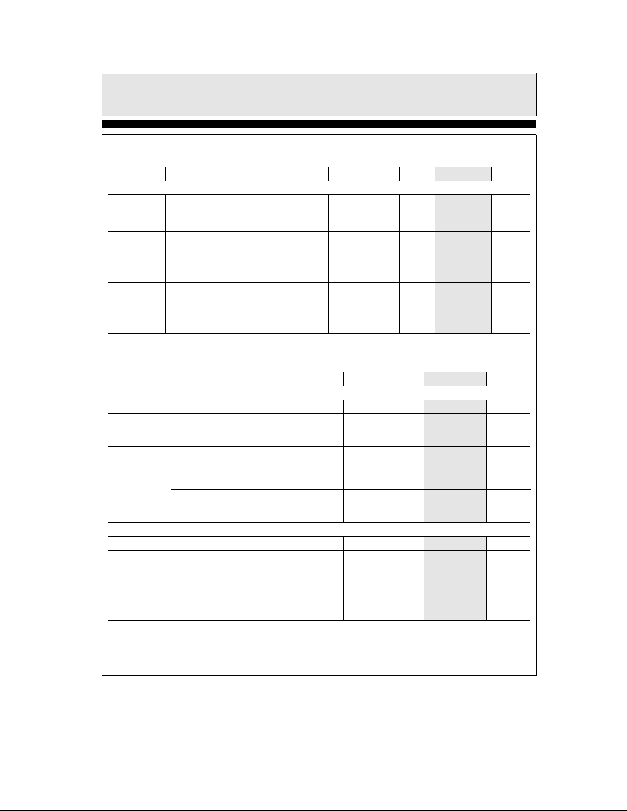
Open Loop DC Electrical Characteristics
e
g
V
S
Parameter Description Temp Min Typ Max Test Level Units
I
S
Video Amplifier Section (Not Restored)
V
OS
I
a
B
I
b
B
R
OL
A
VOL
V
O
I
SC
Sample-And-Hold Section
V
OS
I
B
I
OS
R
IN, DIFF
R
IN, COMM
V
CM
15V; R
L
e
150X,T
e
25§C unless otherwise specified
A
Total Supply Current Full 14 17 II mA
Input Offset Voltage Full 8 70 II mV
a
VINInput Bias Current Full 2 15 II mA
b
VINInput Bias Current Full 30 150 II mA
Transimpedance 25§C 300 V V/mA
Open-Loop Voltage Gain;
e
g
V
OUT
2V
Output Voltage Swing
e
g
V
S
e
g
V
S
15V; R
5V; R
e
2kX
L
e
150X
L
Full 56 65 II dB
Full
Full
g
g
3.0
g
12
13 II V
g
3.5 II V
Short-Circuit Current;
a
VINSet tog2V;bV
to Ground through 1 kX
IN
25§C
g
g
50
g
90
160 II mA
Input Offset Voltage Full 2 10 II mV
Input Bias Current Full 0.5 2.5 II mA
Input Offset Current Full 0.05 0.5 II mA
Input Differential Resistance 25§C 200 V kX
Input Common-Mode Resistance 25§C 100 V MX
Common-Mode Input Range Full
g
g
11
12.5 II V
C
TDis 3.9in
2

EL2090C
100 MHz DC-Restored Video Amplifier
Open Loop DC Electrical Characteristics
e
g
V
S
Parameter Description Temp. Min Typ Max Test Level Units
Sample-And-Hold Section Ð Contd.
A
VOL
CMRR Common-Mode Rejection Ratio
PSRR Power-Supply Rejection Ratio
V
thresh
I
droop
I
charge
V
O
I
SC
Closed Loop AC Electrical Characteristics
e
g
V
S
Parameter Description Min Typ Max Test Level Units
Video Amplifier Section
SR SlewRate; V
BW Bandwidth;b3 dB 75 100 III MHz
Peaking
dG Differential Gain;
di Differential Phase;
Sample-And-Hold Section
BW Gain-Bandwidth Product 1.3 V MHz
DQ Sample to Hold Charge
DT Sample to Hold or Hold to
T
s
Note 1: The logic input is between 0V and 5V, with a 220X resistor in series with the HOLD pin and 39 pF capacitor from HOLD pin
15V; R
L
15V; C
L
to ground.
e
150X,T
e
25§C unless otherwise specified Ð Contd.
A
Large Signal Voltage Gain Full 15k 50k II V/V
V
V
CM
S
e
e
g
11V
g
5V tog15V
Full 75 95 II dB
Full 75 95 II dB
HOLD Pin Logic Threshold Full 0.8 1.4 2.0 II V
Hold Mode Droop Current Full 10 50 II nA
Charge Current Available to
Chold
Output Swing; R
e
2k Full
L
Short-Circuit Current 25§C
e
15 pF; C
(bVIN)e2.5 pF; R
stray
fromb2toa2V 600 V V/ms
OUT
g
1 dB 35 60 III MHz
g
0.1 dB 10 20 III MHz
F
Full
e
e
R
G
300X;R
g
g
g
L
90
10
10
e
g
135 II mA
g
13 II V
g
150X;C
17
hold
g
40 II mA
e
100 pF; T
e
25§C
A
VINfromb0.7V to 0.7V; 0.01 V %
e
F
3.58 MHz
V
fromb0.7V to 0.7V; 0.02 V
IN
Fe3.58 MHz
Injection (Note 1)
Sample Delay Time
Sample to Hold Settling
Time to 2 mV
1.5 5 III pC
20 V ns
200
V
§
ns
TDis 2.3inTDis 3.4in
3

EL2090C
100 MHz DC-Restored Video Amplifier
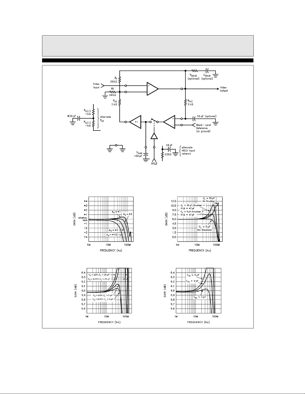
Figure 1. Typical Application (A
Typical Performance Curves
Relative Frequency Response
for Various Gains
Frequency Response Flatness
for Various Load
and Supply Conditions
ea
2)
V
Frequency Response with
Different Loads (A
Frequency Response Flatness vs
C
ea
,A
b
IN
V
ea
V
2
2090– 3
2)
2090– 4
2090– 5
4
 Loading...