EL2003C, EL2033C
100MHz Video Line Driver
EL2003C, EL2033C
Features
• Differential gain 0.1%
• Differential phase 0.1°
• 100mA continuous output current
guaranteed
• Short circuit protected
• Wide bandwidth - 100MHz
• High slew rate - 1200V/µs
• High input impedance - 2MΩ
• Low quiescent current drain
Applications
• Co-ax cable driver
• Flash converter driver
• Video DAC buffer
• Op amp booster
Ordering Information
Part No. Package Tape & Reel Outline#
EL2003CN 8-Pin PDIP MDP0031
EL2003CM 20-Lead SOL MDP0027
EL2033CN 8-Pin PDIP MDP0031
General Description
The EL2003C and EL2033C are general purpose monolithic unity
gain buffers featuring 100MHz, -3dB bandwidth and 4ns small signal
rise time. These buffers are capable of delivering a ±100mA current to
a resistive load and are oscillation free into capacitive loads. In addition, the EL2003C and EL2033C have internal output short circuit
current limiting which will protect the devices under both a DC fault
condition and AC operation with reactive loads. The extremely fast
slew rate of 1200V/µs, wide bandwidth, and high output drive make
the EL2003C and EL2033C ideal choices for closed loop buffer applications with wide band op amps. These same characteristics and
excellent DC performance make the EL2003C and EL2033C excellent
choices for open loop applications such as driving coaxial and twisted
pair cables.
The EL2003C and EL2033C are constructed using Elantec's proprietary dielectric isolation process that produces PNP and NPN
transistors with essentially identical AC and DC characteristics.
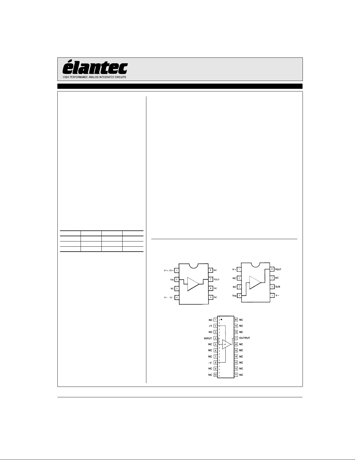
Connection Diagrams
EL2003CN EL2033CN
EL2003CM
Note: All information contained in this data sheet has been carefully checked and is believed to be accurate as of the date of publication; however, this data sheet cannot be a “controlled document”. Current revisions, if any, to these
specifications are maintained at the factory and are available upon your request. We recommend checking the revision level before finalization of your design documentation.
© 2001 Elantec Semiconductor, Inc.
September 1998, Rev F

EL2003C, EL2033C
100MHz Video Line Driver
Absolute Maximum Ratings (T
VSSupply Voltage (V+ - V-) ±18V or 36V
VINInput Voltage ±15V or V
EL2003C, EL2033C
If the input exceeds the ratings shown (or the supplies) or if the input to output voltage
exceeds ±7.5V then the input current must be limited to ±50 mA. See the application
hints for more information.
IINInput Current (See note above) ±50mA
PDPower Dissipation See Curves
The maximum power dissipation depends on package type, ambient temperature and
heat sinking. See the characteristic curves for more details.
= 25°C)
A
Output Short Circuit Duration Continuous
A heat sink is required to keep the junction temperature below the absolute maximum
S
when the output is short circuited.
TAOperating Temperature Range EL2003C/EL2033C -40°C to +85°C
TJOperating Junction Temperature
Metal Can 175°C
Plastic 150°C
TSTStorage Temperature -65°C to +150°C
Important Note:
All parameters having Min/Max specifications are guaranteed. Typ values are for information purposes only. Unless otherwise noted, all tests are at the
specified temperature and are pulsed tests, therefore: TJ = TC = TA.
Electrical Characteristics
VS = ±15V, R
Parameter Description
V
OS
I
IN
R
IN
A
V1
A
V2
A
V3
V
01
V
02
R
OUT
I
OUT
I
S
PSRR Supply Rejection
= 50Ω
S
Test Conditions Limits
IN
Load Temp Min Typ Max
Output Offset Voltage 0 × 25°C -40 5 40 mV
T
Input Current 0 × 25°C, T
MIN
T
Input Resistance ±12V 100Ω 25°C, T
T
, T
MIN
MIN
MAX
MAX
MAX
-50 50 mV
-25 -5 25 µA
-50 50 µA
0.5 2 MΩ
0.05 MΩ
Voltage Gain ±12V 1kΩ 25°C 0.98 0.99 V/V
T
MIN
, T
MAX
0.97 V/V
Voltage Gain ±6V 50Ω 25°C 0.83 0.90 V/V
T
Voltage Gain with V
, T
MIN
= ±5V ±3V 50Ω 25°C 0.82 0.89 V/V
S
MAX
T
, T
MIN
MAX
0.80 V/V
0.79 V/V
Output Voltage Swing ±14V 1kΩ 25°C ±13 ±13.5 V
T
MIN
, T
MAX
±12.5 V
Output Voltage Swing ±12V 100Ω 25°C ±10.5 ±11.3 V
T
MIN
, T
MAX
±10 V
Output Resistance ±2V 50Ω 25°C 7 10 Ω
T
Output Current ±12V
[1]
MIN
25°C ±105 ±230 mA
T
MIN
Supply Current 0 × 25°C, T
[2]
0 × 25°C 60 80 dB
T
T
MIN
, T
, T
MIN
, T
MAX
MAX
MAX
MAX
±100 mA
10 15 mA
50 dB
12 Ω
20 mA
UnitV
2

EL2003C, EL2033C
100MHz Video Line Driver
Electrical Characteristics
VS = ±15V, R
Parameter Description
SR1 Slew Rate
SR2 Slew Rate
THD Distortion @ 1kHz 4 V
1. Force the input to +12V and the output to +10V and measure the output current. Repeat with -12V in and -10V on the output.
2. VS = ±4.5V to ±18V.
3. Slew rate is measured between V
4. Slew rate is measured between V
= 50Ω
S
Test Conditions Limits
[3]
[4]
= +5V and -5V.
OUT
= +2.5V and -2.5V.
OUT
IN
±10V 1kΩ 25°C 600 1200 V/µs
±5V 50Ω 25°C 200 400 V/µs
RMS
Load Temp Min Typ Max
50Ω 25°C 0.2 1 %
EL2003C, EL2033C
UnitV
3

EL2003C, EL2033C
100MHz Video Line Driver
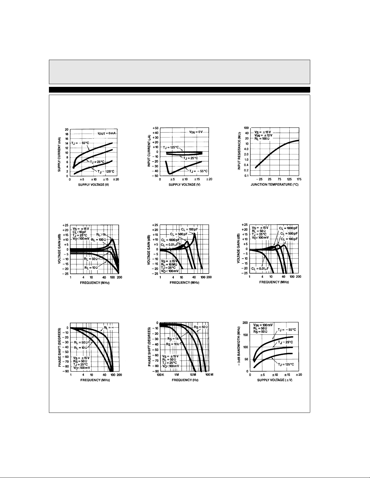
Typical Performance Curves
EL2003C, EL2033C
Quiescent Supply Current
vs Supply Voltage
Voltage Gain vs Frequency
Various Resistive Loads
Input Current
vs Supply Voltage
Voltage Gain vs Frequency
No Resistive Load
Various Capacitive Loads
3Input Resistance
vs Temperature
Voltage Gain vs Frequency
50¾ Resistive Load
Various Capacitive Loads
Phase Shift vs Frequency
Various Resistive Loads
Phase Shift vs Frequency
Various Source Resistors
4
-3 dB Bandwidth
vs Supply Voltage

EL2003C, EL2033C
100MHz Video Line Driver
EL2003C, EL2033C
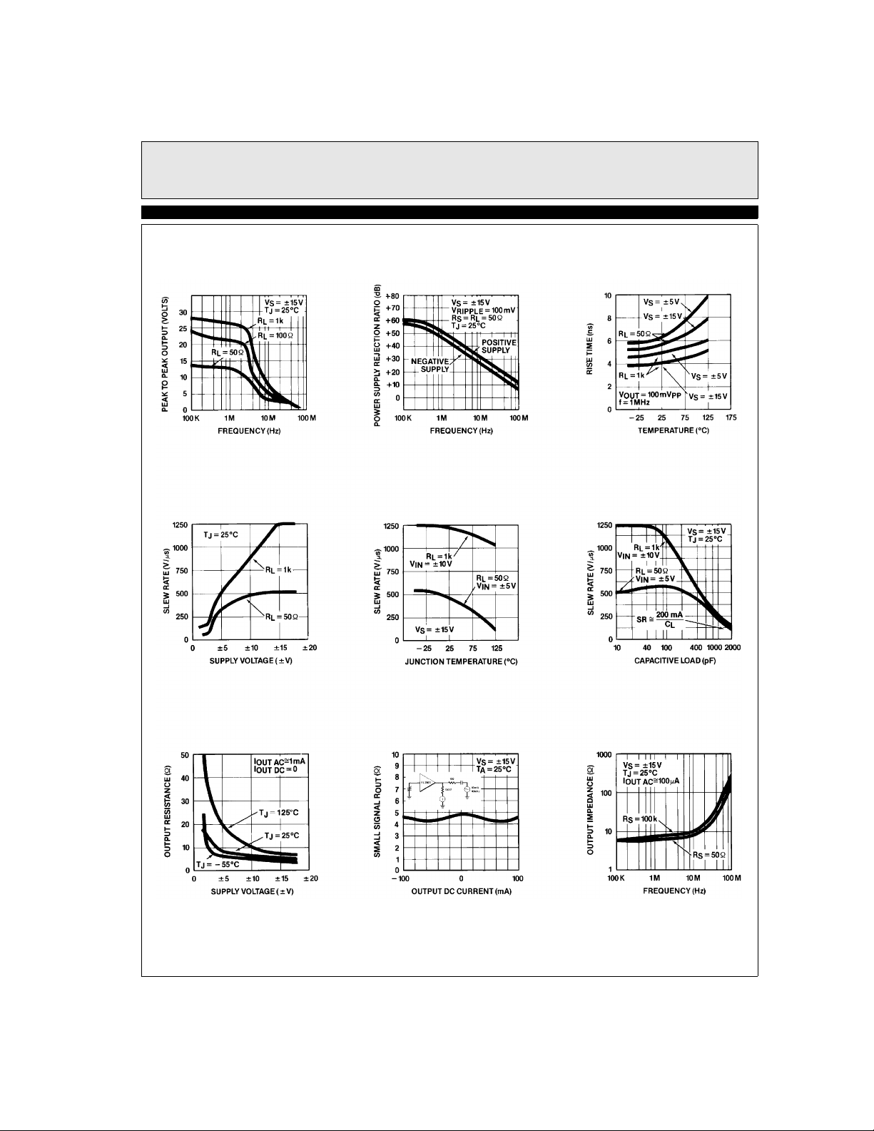
Maximum Undistorted
Output Voltage
vs Frequency
Slew Rate
vs Supply Voltage
Power Supply Rejection
Ratio vs Frequency
Slew Rate
vs Temperature
Rise Time
vs Temperature
Slew Rate
vs Capacitive Load
Output Resistance
vs Supply Voltage
Small Signal
Output Resistance
vs DC Output Current
5
Output Impedance
vs Frequency

EL2003C, EL2033C
100MHz Video Line Driver
EL2003C, EL2033C
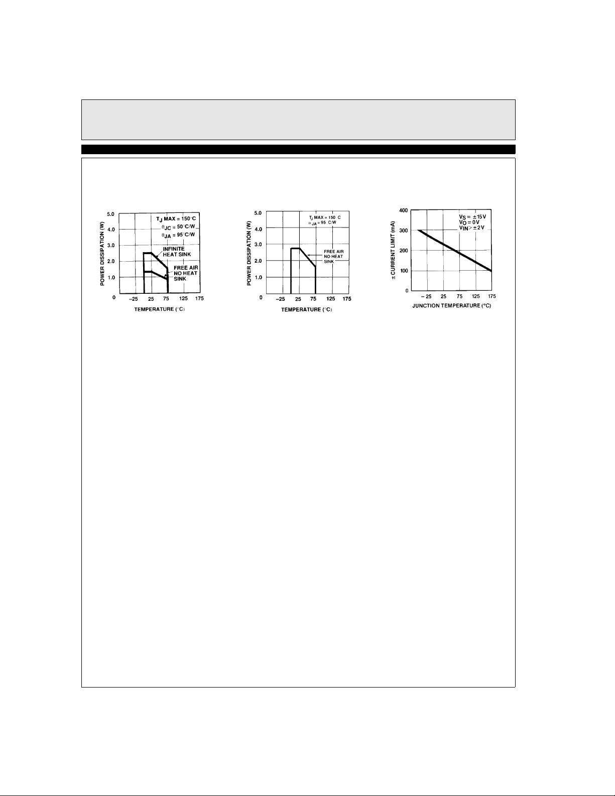
8-Lead Plastic DIP
Maximum Power Dissipation
vs Ambient Temperature
20-Lead SOL
Maximum Power Dissipation
vs Ambient Temperature
Current Limit
vs Temperature
6
 Loading...