ELANT EL1056CM, EL1056ACM Datasheet

EL1056AC/EL1056C
Monolithic High-Speed Pin Driver
EL1056AC/EL1056C March 1993 Rev A
Features
# Wideg12V output levels
# 250 ps dispersion
# 3 ns delay times
# 1V/ns slew rateÐadjustable
# Low overshoot and aberrations in
50X systems
# 3-state output
# Power-down mode reduces
output leakage to nanoamperes
# Overcurrent sense flag available
to protect internal output devices
# Buffered analog inputs
# Differential logic inputs are
compatible with ECL, TTL, and
CMOS
Applications
# Memory testers
# ASIC testers
# Functional board testers
# Analog/digital incoming
component verifiers
# Logic emulators
Ordering Information
Part No. Temp. Range Package Outline
EL1056CM 0§Ctoa75§C 24-Lead MDP0027
EL1056ACM 0§Ctoa75§C 24-Lead MDP0027
Thermal SOL
Thermal SOL
General Description
The EL1056 is designed to drive high-quality test signals into
close or terminated loads. It has a dispersion of 250 ps or less Ð
whether due to signal size or direction of edge. It can output a
very wide 24V output span, encompassing all logic families as
well as analog levels. The EL1056 is fabricated in Elantec’s oxide isolated process, which eliminates the possibility of latch-up
and provides a very durable circuit.
The output can be turned off in two ways; the OE pins allow
the output to be put in a high-impedance state which makes the
output look like a large resistance in parallel with 3 pF, even for
back-driven signals with as much as 2.5V/ms slew rate. The E
pins put the output in an even higher impedance state, guaranteed to 150 nA leakage in the EL1056A. This allows accurate
measurements on the bus without disconnecting the EL1056
with a relay.
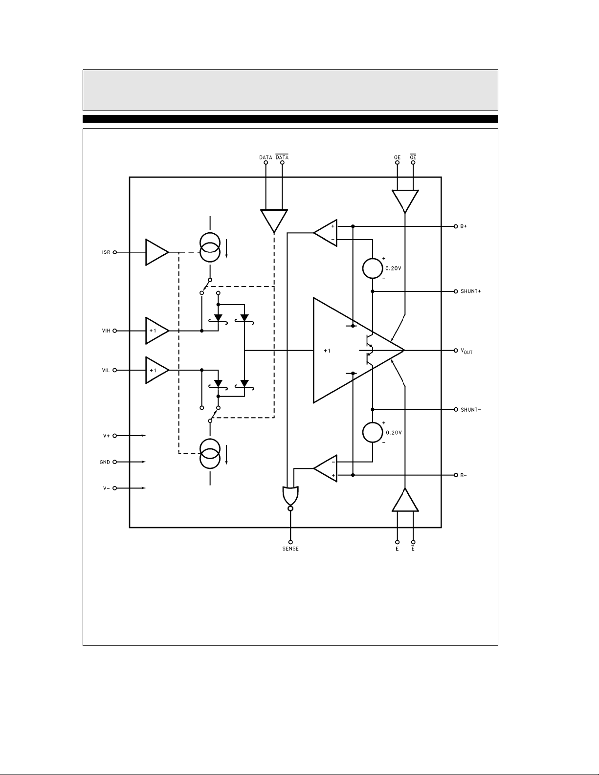
The EL1056 incorporates an output current sense which can
warn the system controller that excessive output current is
flowing. The trip point is set by two external resistors.
Connection Diagram
24-Lead Thermal SOL Package
Ý
*and Heat-spreader
Note: All information contained in this data sheet has been carefully checked and is believed to be accurate as of the date of publication; however, this data sheet cannot be a ‘‘controlled document’’. Current revisions, if any, to these
specifications are maintained at the factory and are available upon your request. We recommend checking the revision level before finalization of your design documentation.
©
1993 Elantec, Inc.
Top View
1056– 1

EL1056AC/EL1056C
Monolithic High-Speed Pin Driver
Absolute Maximum Ratings
V
S
b
V
a
B
b
B
I
SR
V
SR
Shunt
Shunt
Data, Data
OE, OE
Important Note:
All parameters having Min/Max specifications are guaranteed. The Test Level column indicates the specific device testing actually
performed during production and Quality inspection. Elantec performs most electrical tests using modern high-speed automatic test
equipment, specifically the LTX77 Series system. Unless otherwise noted, all tests are pulsed tests, therefore T
Test Level Test Procedure
Voltage between Vaand V
Supply Voltage
Supply Voltage V
Supply Voltage Vbto V
Input Current 0 mA to 3 mA
Input Voltage,
Power-Down Mode
a
Input Voltage (Ba)b5V to B
b
Input Voltage Bbto (Bb)a5V
Input Voltages Vbto Vaor
Input Voltages Vbto Vaor
I 100% production tested and QA sample tested per QA test plan QCX0002.
II 100% production tested at T
III QA sample tested per QA test plan QCX0002.
IV Parameter is guaranteed (but not tested) by Design and Characterization Data.
V Parameter is typical value at T
T
MAX
and T
ba
g
g
A
per QA test plan QCX0002.
MIN
e
(T
25§C)
A
33V
b
to V
INH
b
0.3V toa6V
6V Differential
E, E
18V
a
Sense Output Voltage V
INL
V
INH
V
INL
I
OUT
T
J
a
T
A
T
ST
P
D
6V Differential
e
25§C and QA sample tested at T
e
25§C for information purposes only.
A
Input Voltages Vbto Vaor
g
6V Differential
b
to V
Input Voltage V
Input Voltage Bbto V
Output Current
b
0.3V to B
INL
INH
b
60 mA toa60 mA
a
0.3V
Junction Temperature 150§C
Operating Ambient Temperature
Range
Storage Temperature
Power Dissipation (T
(See Curves) 3.1W
e
25§C,
A
e
25§C)
A
b
b
65§Ctoa150§C
e
e
T
J
C
0§Ctoa75§C
TA.
a
a
DC Electrical Characteristics
e
T
25§C, VaeBae15V, VbeB
A
b
0.8V. I
SR
e
800 mA. V
INH
e
Parameter Description Min Typ Max
I
S
(Va)a(Ba), (Vb)a(Bb) Supply Currents 52 60 I mA
IS, dis (Va)a(Ba), (Vb)a(Bb) Supply Currents, Disabled 17 25 I mA
I
VINH
I
VINL
I
DATA
I
OE
I
E
V
SR
I
SHUNT
V
SHUNT
I
SENSE
V
OS
a
a
,I
SHUNT
,V
SHUNT
OE Input Current
E Input Current
Voltage at ISRPin 0 20 40 I mV
b
Sense Threshold at Shunts 160 200 250 I mV
b
Sense Output Currents 1 1.5 2 I mA
Output Offset, Data High, V
5V, V
beb
INL
eb
10V, R
1.6V
Data Low, V
SHUNT
INH
INL
e
e
e
a
0V, V
0V, V
R
SHUNT
INL
INH
e
6.5X, no load. Data, E, and OE fromb1.6V to
b
b
b
20
320 I mA
b
20 2 20 I mA
b
30b15 30 I mA
b
30b14 30 I mA
b
20 7 20 I mA
47 I mA
eb
e
1.6V
5V
b
50 50 I mV
b
100 100 I mV
Test
Level
Units
TDis 2.7in
2

EL1056AC/EL1056C
Monolithic High-Speed Pin Driver
DC Electrical Characteristics
e
T
25§C, VaeBae15V, VbeB
A
b
0.8V. I
SR
e
800 mA. V
INH
e
Parameter Description Min Typ Max
Eg Gain Error Data High, V
Data Low, V
NL Gain Nonlinearity Data High, V
PSRR Power Supply Rejection Ratio of V
a,Bb
to B
, Shunta, or ShuntbPotential
Ro, en Output Resistance, Enabled, Il
Ro, dis Output Resistance, Output Disabled, V
Io, dis Output Current, Output, Disabled, V
Io, off Output Leakage, E Low, (Shut-Down), V
beb
5V, V
INL
INH
INH
Data Low, V
eb
from 0V to 5V, V
e
Ð Contd.
10V, R
SHUNT
e
R
a
SHUNT
1.6V
eb
5V, V
INH
e
INH
OUT
e
g
20 mA 4.5 6 7.5 I X
O
INL
fromb5V to 0V, No Load
INL
from 0V to 10V, V
5V, V
INL
INL
fromb10V to 0V, No Load 0.06 V %
with Respect
eb
1.6V tob5V, EL1056C 20K 100K
O
e
0V
e
0V, EL1056C
O
EL1056AC
e
6.5X, no load. Data, E, and OE fromb1.6V to
b
1.6V, No Load
eb
1.6V, No Load 0.04 V %
b
1.5b0.6 0 I %
b
1.5b0.6 0 I %
2.2 V mV/V
EL1056AC 100K 200K
b
20 5 20 I mA
b
20 20 I mA
b
150 150 I nA
Test
Level
AC Electrical Characteristics
e
T
25§C, VaeB
A
included at output. Data E, and OE from
b
1.6V, CMOS swing defined by V
Parameter Description Min Typ Max
T
PD
Dis Propagation Delay Dispersion
SR Output Slew Rate, CMOS Swing, 20% –80% 0.8 1 1.2 I V/ns
SR
sym
TR Output Rise Time, ECL Swing, 20% –80% 2.2 V ns
OS Output Overshoot
T
dis
T
en
Co, dis Output Capacitance in Disable 3 V pF
T
off
T
on
Co, off Output Capacitance in Power-Down 50 V pF
T
sense
aea
15V, VbeB
INH
beb
b
1.6V tob0.8V. I
e
5V and V
10V, R
SHUNT
e
0V. Propagation delay is measured at 0.4V movement of output.
INL
e
R
a
SHUNT
e
800 mA. ECL swing is defined by V
SR
b
e
6.5X.R
e
500X.50Xa22 pF snubber
L
INH
eb
0.8V and V
Test
Level
Propagation Delay, CMOS Swing 1.0 3.0 4.5 I ns
Due to Output Edge Direction 250 450 I ps
From ECL to CMOS Swings 250 450 I ps
Due to Repetition Rate 80 V ps
Slew Rate Symmetry 3 10 I %
CMOS Swing 190 500 I mV
ECL Swing (I
e
350 mA) 65 V mV
SR
Output Disable Delay Time 4.7 6.5 I ns
Output Enable Delay Time 6.0 8.5 I ns
Power-Down Delay Time 0.5 V ms
Power-On Delay Time 90 V ns
Comparator Delay Time Ð Switching ON 1.5 V ms
Switching Off 0.4 V ms
Units
I X
e
INL
Units
TDis 2.3inTDis 3.6in
3

EL1056AC/EL1056C
Monolithic High-Speed Pin Driver
Block Diagram
1056– 5
4

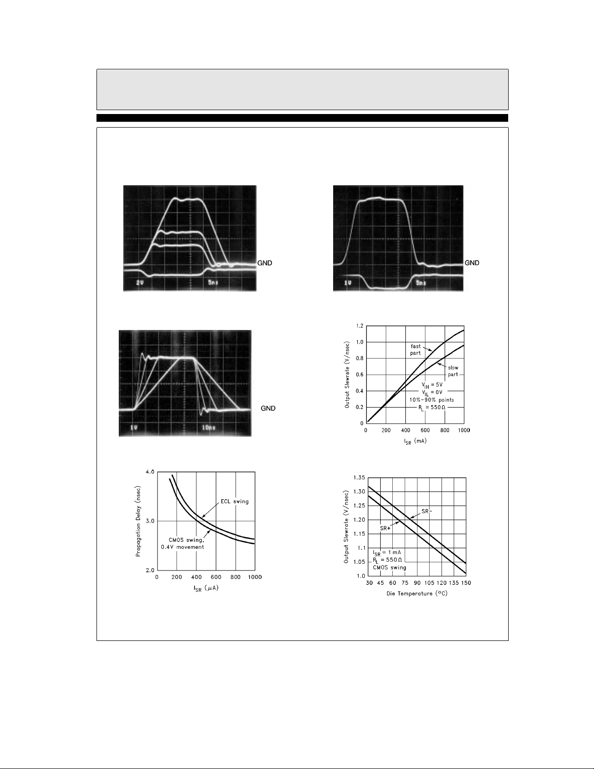
Typical Performance Curves
10V, CMOS, TTL, and ECL
Outputs into 550X Load
EL1056AC/EL1056C
Monolithic High-Speed Pin Driver
CMOS and ECL Outputs As Seen
at the End of an Unterminated
Cable, Backmatched at Driver
CMOS Output at I
SR
e
100 mA,
200 mA, 400 mA, and 1000 mA
Propagation Delay vs I
1056– 6
Output Slewrate vs I
(Two Samples)
1056– 8
SR
Output Slewrate vs
Die Temperature
SR
1056– 7
1056– 9
1056– 10
1056– 11
5
 Loading...