


EL1056AC/EL1056C
Monolithic High-Speed Pin Driver
EL1056AC/EL1056C March 1993 Rev A
Features
# Wideg12V output levels
# 250 ps dispersion
# 3 ns delay times
# 1V/ns slew rateÐadjustable
# Low overshoot and aberrations in
50X systems
# 3-state output
# Power-down mode reduces
output leakage to nanoamperes
# Overcurrent sense flag available
to protect internal output devices
# Buffered analog inputs
# Differential logic inputs are
compatible with ECL, TTL, and
CMOS
Applications
# Memory testers
# ASIC testers
# Functional board testers
# Analog/digital incoming
component verifiers
# Logic emulators
Ordering Information
Part No. Temp. Range Package Outline
EL1056CM 0§Ctoa75§C 24-Lead MDP0027
EL1056ACM 0§Ctoa75§C 24-Lead MDP0027
Thermal SOL
Thermal SOL
General Description
The EL1056 is designed to drive high-quality test signals into
close or terminated loads. It has a dispersion of 250 ps or less Ð
whether due to signal size or direction of edge. It can output a
very wide 24V output span, encompassing all logic families as
well as analog levels. The EL1056 is fabricated in Elantec’s oxide isolated process, which eliminates the possibility of latch-up
and provides a very durable circuit.
The output can be turned off in two ways; the OE pins allow
the output to be put in a high-impedance state which makes the
output look like a large resistance in parallel with 3 pF, even for
back-driven signals with as much as 2.5V/ms slew rate. The E
pins put the output in an even higher impedance state, guaranteed to 150 nA leakage in the EL1056A. This allows accurate
measurements on the bus without disconnecting the EL1056
with a relay.
The EL1056 incorporates an output current sense which can
warn the system controller that excessive output current is
flowing. The trip point is set by two external resistors.
Connection Diagram
24-Lead Thermal SOL Package
Ý
*and Heat-spreader
Note: All information contained in this data sheet has been carefully checked and is believed to be accurate as of the date of publication; however, this data sheet cannot be a ‘‘controlled document’’. Current revisions, if any, to these
specifications are maintained at the factory and are available upon your request. We recommend checking the revision level before finalization of your design documentation.
©
1993 Elantec, Inc.
Top View
1056– 1
EL1056AC/EL1056C
Monolithic High-Speed Pin Driver
Absolute Maximum Ratings
V
S
b
V
a
B
b
B
I
SR
V
SR
Shunt
Shunt
Data, Data
OE, OE
Important Note:
All parameters having Min/Max specifications are guaranteed. The Test Level column indicates the specific device testing actually
performed during production and Quality inspection. Elantec performs most electrical tests using modern high-speed automatic test
equipment, specifically the LTX77 Series system. Unless otherwise noted, all tests are pulsed tests, therefore T
Test Level Test Procedure
Voltage between Vaand V
Supply Voltage
Supply Voltage V
Supply Voltage Vbto V
Input Current 0 mA to 3 mA
Input Voltage,
Power-Down Mode
a
Input Voltage (Ba)b5V to B
b
Input Voltage Bbto (Bb)a5V
Input Voltages Vbto Vaor
Input Voltages Vbto Vaor
I 100% production tested and QA sample tested per QA test plan QCX0002.
II 100% production tested at T
III QA sample tested per QA test plan QCX0002.
IV Parameter is guaranteed (but not tested) by Design and Characterization Data.
V Parameter is typical value at T
T
MAX
and T
ba
g
g
A
per QA test plan QCX0002.
MIN
e
(T
25§C)
A
33V
b
to V
INH
b
0.3V toa6V
6V Differential
E, E
18V
a
Sense Output Voltage V
INL
V
INH
V
INL
I
OUT
T
J
a
T
A
T
ST
P
D
6V Differential
e
25§C and QA sample tested at T
e
25§C for information purposes only.
A
Input Voltages Vbto Vaor
g
6V Differential
b
to V
Input Voltage V
Input Voltage Bbto V
Output Current
b
0.3V to B
INL
INH
b
60 mA toa60 mA
a
0.3V
Junction Temperature 150§C
Operating Ambient Temperature
Range
Storage Temperature
Power Dissipation (T
(See Curves) 3.1W
e
25§C,
A
e
25§C)
A
b
b
65§Ctoa150§C
e
e
T
J
C
0§Ctoa75§C
TA.
a
a
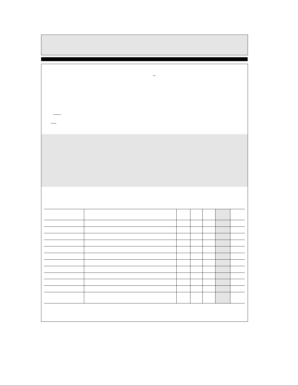
DC Electrical Characteristics
e
T
25§C, VaeBae15V, VbeB
A
b
0.8V. I
SR
e
800 mA. V
INH
e
Parameter Description Min Typ Max
I
S
(Va)a(Ba), (Vb)a(Bb) Supply Currents 52 60 I mA
IS, dis (Va)a(Ba), (Vb)a(Bb) Supply Currents, Disabled 17 25 I mA
I
VINH
I
VINL
I
DATA
I
OE
I
E
V
SR
I
SHUNT
V
SHUNT
I
SENSE
V
OS
a
a
,I
SHUNT
,V
SHUNT
OE Input Current
E Input Current
Voltage at ISRPin 0 20 40 I mV
b
Sense Threshold at Shunts 160 200 250 I mV
b
Sense Output Currents 1 1.5 2 I mA
Output Offset, Data High, V
5V, V
beb
INL
eb
10V, R
1.6V
Data Low, V
SHUNT
INH
INL
e
e
e
a
0V, V
0V, V
R
SHUNT
INL
INH
e
6.5X, no load. Data, E, and OE fromb1.6V to
b
b
b
20
320 I mA
b
20 2 20 I mA
b
30b15 30 I mA
b
30b14 30 I mA
b
20 7 20 I mA
47 I mA
eb
e
1.6V
5V
b
50 50 I mV
b
100 100 I mV
Test
Level
Units
TDis 2.7in
2

EL1056AC/EL1056C
Monolithic High-Speed Pin Driver
DC Electrical Characteristics
e
T
25§C, VaeBae15V, VbeB
A
b
0.8V. I
SR
e
800 mA. V
INH
e
Parameter Description Min Typ Max
Eg Gain Error Data High, V
Data Low, V
NL Gain Nonlinearity Data High, V
PSRR Power Supply Rejection Ratio of V
a,Bb
to B
, Shunta, or ShuntbPotential
Ro, en Output Resistance, Enabled, Il
Ro, dis Output Resistance, Output Disabled, V
Io, dis Output Current, Output, Disabled, V
Io, off Output Leakage, E Low, (Shut-Down), V
beb
5V, V
INL
INH
INH
Data Low, V
eb
from 0V to 5V, V
e
Ð Contd.
10V, R
SHUNT
e
R
a
SHUNT
1.6V
eb
5V, V
INH
e
INH
OUT
e
g
20 mA 4.5 6 7.5 I X
O
INL
fromb5V to 0V, No Load
INL
from 0V to 10V, V
5V, V
INL
INL
fromb10V to 0V, No Load 0.06 V %
with Respect
eb
1.6V tob5V, EL1056C 20K 100K
O
e
0V
e
0V, EL1056C
O
EL1056AC
e
6.5X, no load. Data, E, and OE fromb1.6V to
b
1.6V, No Load
eb
1.6V, No Load 0.04 V %
b
1.5b0.6 0 I %
b
1.5b0.6 0 I %
2.2 V mV/V
EL1056AC 100K 200K
b
20 5 20 I mA
b
20 20 I mA
b
150 150 I nA
Test
Level
AC Electrical Characteristics
e
T
25§C, VaeB
A
included at output. Data E, and OE from
b
1.6V, CMOS swing defined by V
Parameter Description Min Typ Max
T
PD
Dis Propagation Delay Dispersion
SR Output Slew Rate, CMOS Swing, 20% –80% 0.8 1 1.2 I V/ns
SR
sym
TR Output Rise Time, ECL Swing, 20% –80% 2.2 V ns
OS Output Overshoot
T
dis
T
en
Co, dis Output Capacitance in Disable 3 V pF
T
off
T
on
Co, off Output Capacitance in Power-Down 50 V pF
T
sense
aea
15V, VbeB
INH
beb
b
1.6V tob0.8V. I
e
5V and V
10V, R
SHUNT
e
0V. Propagation delay is measured at 0.4V movement of output.
INL
e
R
a
SHUNT
e
800 mA. ECL swing is defined by V
SR
b
e
6.5X.R
e
500X.50Xa22 pF snubber
L
INH
eb
0.8V and V
Test
Level
Propagation Delay, CMOS Swing 1.0 3.0 4.5 I ns
Due to Output Edge Direction 250 450 I ps
From ECL to CMOS Swings 250 450 I ps
Due to Repetition Rate 80 V ps
Slew Rate Symmetry 3 10 I %
CMOS Swing 190 500 I mV
ECL Swing (I
e
350 mA) 65 V mV
SR
Output Disable Delay Time 4.7 6.5 I ns
Output Enable Delay Time 6.0 8.5 I ns
Power-Down Delay Time 0.5 V ms
Power-On Delay Time 90 V ns
Comparator Delay Time Ð Switching ON 1.5 V ms
Switching Off 0.4 V ms
Units
I X
e
INL
Units
TDis 2.3inTDis 3.6in
3
EL1056AC/EL1056C
Monolithic High-Speed Pin Driver
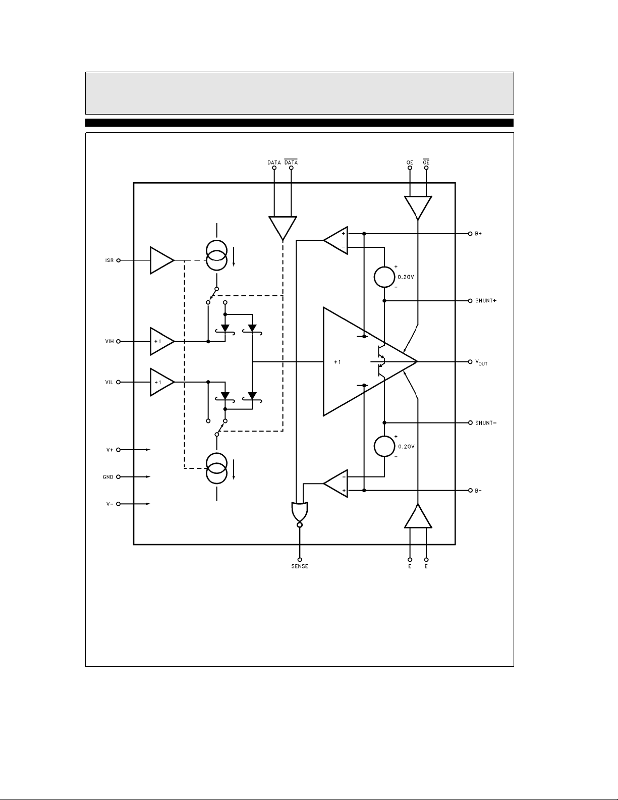
Block Diagram
1056– 5
4
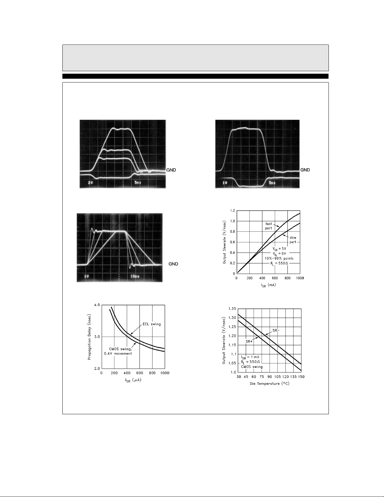
Typical Performance Curves
10V, CMOS, TTL, and ECL
Outputs into 550X Load
EL1056AC/EL1056C
Monolithic High-Speed Pin Driver
CMOS and ECL Outputs As Seen
at the End of an Unterminated
Cable, Backmatched at Driver
CMOS Output at I
SR
e
100 mA,
200 mA, 400 mA, and 1000 mA
Propagation Delay vs I
1056– 6
Output Slewrate vs I
(Two Samples)
1056– 8
SR
Output Slewrate vs
Die Temperature
SR
1056– 7
1056– 9
1056– 10
1056– 11
5

EL1056AC/EL1056C
Monolithic High-Speed Pin Driver
Typical Performance Curves
Propagation Delay Change
with Die Temperature
Output Edge Dispersion vs
Temperature
Ð Contd.
1056– 12
Change in Propagation Delay
with Power Supply Headroom
Edge Dispersion vs I
SR
1056– 13
Minimum Output Pulse Width
1056– 14
1056– 16
1056– 15
Output Offset vs I
SR
1056– 17
6

EL1056AC/EL1056C
Monolithic High-Speed Pin Driver
Typical Performance Curves
Tristate Turn-off Waveforms
Power-Down Disable Waveforms
Supply Current vs I
SR
Ð Contd.
1056– 18
1056– 20
Tristate Turn-on Waveforms
Power-Down Enable Waveforms
Total Supply Current vs
Supply Voltage
1056– 19
1056– 21
1056– 22
1056– 23
7

EL1056AC/EL1056C
Monolithic High-Speed Pin Driver
Typical Performance Curves
Mounted Thermal Resistance of
Package vs Airflow Speed
1056– 24
EL1056 Used in CMOS and TTL Systems
Ð Contd.
Package Power Dissipation
vs Ambient Temperature
1056– 25
Sense Comparator Delay
vs Overdrive
1056– 26
1056– 4
8

Monolithic High-Speed Pin Driver
Applications Information
Functional Description
The EL1056 is a fully integrated pin driver for
automatic test systems. Pin drivers are essentially pulse generators whose high and low levels can
be externally programmed and accurately switched in time, as well as incorporating an output
switch to disconnect the driver from a measurement bus. Additionally, the EL1056 has programmable slewrate.
Control Voltage Inputs
The analog level inputs are named V
V
, and the output replicates them as con-
INL
trolled by logic inputs. The analog inputs are
buffered and have bandwidths of 35 MHz and
slewrates of 25V/ms. For full slewrate, 4V of
headroom should be given to the inputs, that is
V
should be 4V less than Vaor Ba, and
INH
V
should be 4V more positive than Vbor
INL
b
B
. At lower slewrates (I
e
500 mA or less),
SR
3V of headroom will suffice. Insufficient headroom causes distorted output waveforms or delay
errors in output transitions. V
in voltage than V
, but the output will not fol-
INL
may be lower
INH
low the control logic correctly. Furthermore,
V
should be 200 mV more positive than V
INH
(the minimum output amplitude) for accurate
switching.
Logic Inputs
The logic inputs are all differential types, with
both NPN and PNP transistors connected to
each terminal. They are optimized for differential
ECL drive, which optimizes
atob
time matching. Larger logic levels can introduce
feedthrough glitches into the output waveform.
For CMOS input logic levels, an ECL output
waveform will show feedthrough when the
input risetime is shorter than 8 ns, differential or
single-ended. CMOS output swings show less aberration, and the EL1056 can toleratea4ns
single-ended risetime or 2 ns risetime for differential inputs. Attenuating CMOS or TTL inputs
to 1 Vp-p will eliminate all logic feedthrough as
shown in Figure 1.
and
INH
INL
edge delay
EL1056AC/EL1056C
1056– 2
Alternate Logic Interface
Figure 1
Slewrate Control
The slewrate is controlled by the ISRinput. This
is a current input and scales the output slewrate
by a nominal 1.25V/ns/mA. The slewrate maintains calibration and symmetry to at least as slow
as 0.2V/ns. The practical upper end of I
1 mA, and supply current increases with increasing I
.
SR
The I
control can be used to adjust individual
SR
pin drivers to a system standard, by adjusting
the value of its series resistor. Slewrate can also
be slowed to reduce output ringing and crosstalk.
With ECL output swings, there is not enough
voltage excursion to incur slewrate delays to 50%
logic threshold. The risetime, delays, and dispersions do not degrade with reasonably reduced
I
, and overshoot will reduce markedly. An I
SR
of 350 mA produces a very good ECL output, and
driver dissipation is also reduced.
1056– 3
SR
is
SR
9

EL1056AC/EL1056C
Monolithic High-Speed Pin Driver
Applications Information
The I
transistor whose base is biased a diode below
ground (see Figure 2). Thus, the I
like a low impedance for positive input currents,
and is biased close to ground. A protection diode
absorbs negative currents, and the input PNP
will not conduct. In power-down mode, the PNP
releases its current sink and the external circuit
must not present more than 6V to the disabled
I
SR
will occur within the driver. A signal diode or
zener can be used to clamp the I
tive input voltages if the voltage on the I
tor is potentially greater than 6V when the driver
is in power-down mode.
pin is connected to the emitter of a PNP
SR
input, or emitter-base damage to the NPN
Ð Contd.
input looks
SR
input for posi-
SR
SR
resis-
Output Stage–Tristate Mode
In tristate mode (OE low) the output transistors
have their emitter-base junctions reverse-biased
by a diode voltage. This turn-off voltage is in fact
provided by an internal buffer whose input is
connected to the output pin (see Figure 3). Transistors Q1 – Q4 form the output buffer in normal
mode. The tristate mode buffer Q5 –Q8 replicates
externally impressed voltages from the output
pin onto the internal schottky switch node. They
also turn off Q1 –Q4 by a reverse diode voltage
between bases and emitters, effectively bootstrapping the internal voltages, so that no transistor’s base-emitter junction is reverse-biased by
a damaging potential. Another benefit is that the
capacitance seen at the output in tristate mode is
reduced.
Because the tristate buffer’s input is connected to
the output terminal, the output is quite ‘‘alive’’
during tristate. For instance, the input bias current of the buffer is seen as the tristate ‘‘leakage’’,
and its variation with applied voltage becomes
tristate input impedance.
The tristate input current is like a current source,
and it can drag an output to unpredictable voltages. It is not a danger to connect a tristated output that has drifted to, say,
a device to be tested. The tristate output current
will simply comply with whatever voltage the
connected part normally establishes.
The tristate input impedance is also quite active
over frequency. The output can oscillate when
presented with resonant or inductive impedances.
To prevent this, a snubber should be connected
from output to ground, consisting of a resistor in
series with a small capacitor. The snubber can
also reduce the reflections of the coaxial line
when driven from the far end, since the line appears to have an open termination during tristate. Typical values for the resistor are 50X to
75X, and 12 pF to 22 pF for the series capacitor.
The effect of the snubber is to ‘‘de-Q’’ resonances
at the output.
b
6V to a logic pin of
Figure 2. ISRPin Circuitry
10
1056– 27

EL1056AC/EL1056C
Monolithic High-Speed Pin Driver
Applications Information
Ð Contd.
Figure 3. Output Stage Circuit in Tristate Mode
Output Stage–Normal Mode
Capacitive loads can cause the output stage to
ring. Little ringing occurs for loads less than
25 pF, but substantial ringing for more than
40 pF. Terminated transmission lines cause no
ringing, and actually suppress it as a snubber
does. A terminated line draws heavy DC current,
however, and greatly raises dissipation.
Driving a back-terminated line also causes little
ringing and does not cause DC dissipation. The
series matching resistor between the EL1056 output and a back-terminated line also serves to isolate the driver from capacitive loads and shortcircuits. The slewrate of the driver slows by
about 10% when driving a 50X back-matched
1056– 28
line, as seen at the end of the line. The snubber
can be on either side of the back-match resistor.
When placed on the line side it creates a highfrequency termination for the line when the
driver is tristated, but it slows the output smallsignal risetime by about 10% (although not slewrate). When placed on the driver side of the backmatch resistor, no speed reduction occurs in
normal mode but the cable is more poorly terminated in tristate.
The transient currents that occur when driving
capacitive or back-matched loads can be very
high, approaching 100 mA. The driver is capable
of outputting a peak of 140 mA, but long-term
11

EL1056AC/EL1056C
Monolithic High-Speed Pin Driver
Applications Information
load currents must be limited to 60 mA. Shortcircuits can rapidly destroy the EL1056, although
the part will survive for 20 ms periods. If there is
the possibility of output load fault the overcurrent sense circuitry should be used to signal
alarm to the controlling system, which should ultimately activate the tristate mode to relieve the
output stage. Driving large static currents also
raises internal dissipation and should be part of
the thermal budget.
Ð Contd.
The collectors of the output transistors are connected to the Shunt terminals, and the output
stage drivers’ collectors are connected to the B
and Bbterminals (see Figure 4). The Shunt
lines can have transient currents as high as
120 mA and are separated from the V
terminals to keep switching noise out of the control and logic circuitry. A bypass capacitor
should be connected to the B
nals.
a
a
and Bbtermi-
and V
a
b
Figure 4. Output Stage in Normal Mode
12
1056– 29

Applications Information
Ð Contd.
Overcurrent Protection
The sense comparators are available to alert the
test system’s controller that the driver is outputting excessive current. Shunt resistors are connected from B
When the internal comparators sense more than
a nominal 200 mV drop on the shunts, they cause
a 1.5 mA current to be sunk from the Sense terminal. The comparators are of ‘‘slow attack, fast
decay’’ design, so that transient load currents will
not trigger a sense output; only a sustained overcurrent will.
The sense resistors must not be inductive, and
the skin resistance of long, narrow connections
between Shunt and B
sient voltages that produce output overshoot
(but not ringing).
The Sense output is simply a switched current
source connected to V
face to CMOS, TTL, or ECL inputs. For CMOS
and TTL, it can be connected to a pull-up resistor
a
to
5V of 10K value. This establishes a logic
high value, and a clamp diode (internal to TTL)
establishes a low level of
should be available to provide a static logic high
level. An 820X pull-up resistor is wired to that
output. The logic low will be more negative than
is usual for ECL, but this will cause no problem.
In all cases, multiple Sense outputs may be connected together from many drivers to effect a
wired-or function.
A further protection scheme is to provide a series
resistor from B
resistor serves to limit the output fault current
by allowing B
heavy load. This also reduces the dissipation on
the output transistors for valid loads. Because
a
to Shuntaand Bbto Shuntb.
a
or Bbcan cause tran-
b
. It can be used to inter-
b
0.6V. For ECL, a gate
a
to Vaand Bbto Vb. The
a
and Bbvoltages to sag under
EL1056AC/EL1056C
Monolithic High-Speed Pin Driver
a
and Bbare separately bypassed, these volt-
B
ages will sustain under transient loads and dynamics will not be affected.
Output Accuracy
The accuracy of the output voltage depends on
several factors. The first is the gain error from
V
or V
INH
error is nominally
of a percent variation between parts. The second
is supply rejection. If the B
b
Shunt
by Elantec to test the part, there will be about
2.2 mV systematic shift in output offset per volt
of supply variation. The V
have much less influence on output error. Finally, there is a random V
data table.
Of course, the finite output impedance of the
EL1056 will cause additional output error when
the driver is loaded.
Power-Down
The EL1056 incorporates a power-down feature
that drastically reduces power consumption of an
unused driver and also drops the output leakage
current to nanoamperes (‘‘A’’ grade only). The
output is not a low capacitance in this mode,
however, and transients driven from the cable
can momentarily turn on the output transistors.
Power-down is intended to allow the switching of
accurate DC meters onto the bus without having
to relay out the driver’s leakage current. It takes
about 40 ms for the output leakage to sag to nanoamperes, but this is still much faster than relays or voltmeters.
Power-down is controlled by the E and E
ential inputs. There is no problem with logic amplitude or slewrate, and input resistor networks
are not needed.
to the output, unloaded. The gain
INL
voltages are different from those used
b
0.6%, and has a few tenths
a,Bb
, Shunta,or
a
and Vbsupplies
error as specified in the
OS
differ-
13

EL1056AC/EL1056C
Monolithic High-Speed Pin Driver
Power Down
Supply and Input Bypassing
The Va,Ba,Vb, and Bbleads should be bypassed very closely with 0.1 mF capacitors, preferably chip type. There should be a wide ground
plane between bypasses, and this can be the heatsink copper. It is wise to also have a 4.7 mF tantalum bypass capacitor within a couple of inches to
the driver.
The logic inputs are active device bases, and can
oscillate if presented with inductive lines. A local
resistor of 1000X or less to ground will suffice in
de-Q’ing any resonance. A 100 pF or larger capacitor can also serve as a bypass.
Ð Contd.
Thermal Considerations
The package of the EL1056 includes two fused
leads on each side which are connected to the internal die mounting metal. Heat generated in the
die flows through the mounting pad to the fused
leads, and then to the circuit-board copper,
achieving a thermal resistance to air around
40
/W. Characterization curves show the thermal
§
resistance versus airflow rate. Consult the
EL1056 Demonstration Board literature for a
suggested board pattern. Note that thicker layers
of copper than we used improves the thermal resistance further, to a limit of 22
nite heatsink’’ directly soldered to the fused
leads.
As a practical limit, the die temperature should
be kept to 125
to retain optimum timing accuracies.
C rather than the allowable 150§C
§
C/W for an ‘‘infi-
§
14

BLANK
15

EL1056AC/EL1056C
Monolithic High-Speed Pin Driver
EL1056AC/EL1056CMarch 1993 Rev A
General Disclaimer
Specifications contained in this data sheet are in effect as of the publication date shown. Elantec, Inc. reserves the right to make changes
in the circuitry or specifications contained herein at any time without notice. Elantec, Inc. assumes no responsibility for the use of any
circuits described herein and makes no representations that they are free from patent infringement.
WARNING Ð Life Support Policy
Elantec, Inc. products are not authorized for and should not be
used within Life Support Systems without the specific written
consent of Elantec, Inc. Life Support systems are equipment in-
Elantec, Inc.
1996 Tarob Court
Milpitas, CA 95035
Telephone: (408) 945-1323
(800) 333-6314
Fax: (408) 945-9305
European Office: 44-71-482-4596
tended to support or sustain life and whose failure to perform
when properly used in accordance with instructions provided can
be reasonably expected to result in significant personal injury or
death. Users contemplating application of Elantec, Inc. products
in Life Support Systems are requested to contact Elantec, Inc.
factory headquarters to establish suitable terms & conditions for
these applications. Elantec, Inc.’s warranty is limited to replacement of defective components and does not cover injury to persons or property or other consequential damages.
Printed in U.S.A.16
 Loading...