

ELAN Microelectronics Corporation EM78612 Specification

EM78612
Product
Specification
DOC. V
ERSION
1.0
ELAN MICROELECTRONICS CORP.
March 2006

Trademark Acknowledgments:
IBM is a registered trademark and PS/2 is a trademark of IBM.
Windows is a trademark of Microsoft Corporation.
ELAN and ELAN logo are trademarks of ELAN Microelectronics Corporation.
Copyright
© 2006 by ELAN Microelectronics Corporation
All Rights Reserved
Printed in Taiwan
The contents of in this specification are subject to change without notice. ELAN Microelectronics assumes no
responsibility concerning the accuracy, adequacy, or completeness of this specification. ELAN Microelectronics
makes no commitment to update, or to keep current the information and material contained in this specification.
Such information and material may change to conform to each confirmed order.
In no event shall ELAN Microelectronics be made responsible to any claims attributed to errors, omissions, or
other inaccuracies in the information or material contained in this specification. ELAN Microelectronics shall not
be liable for direct, indirect, special incidental, or consequential damages arising out of the use of such information
or material.
The software (if any) described in this specification is furnished under a license or nondisclosure agreement, and
may be used or copied only in accordance with the terms of such agreement.
ELAN Microelectronics products are not intended for use in life support appliances, devices, or systems. Use of
ELAN Microelectronics product in such applications is not supported and is prohibited.
NO PART OF THIS SPECIFICATION MAY BE REPRODUCED OR TRANSMITTED IN ANY FORM OR BY
ANY MEANS WITHOUT THE EXPRESS WRITTEN PERMISSION OF ELAN MICROELECTRONICS.
Headquarters:
No. 12, Innovation Road 1
Science-based Industrial Park
Hsinchu, Taiwan 308
Tel: +886 3 563-9977
Fax: +886 3 563-9966
http://www.emc.com.tw
Hong Kong:
Elan (HK) Microelectronics
Corporation, Ltd.
Rm. 1005B, 10/F Empire Centre
68 Mody Road, Tsimshatsui
Kowloon , HONG KONG
Tel: +852 2723-3376
Fax: +852 2723-7780
elanhk@emc.com.hk
USA:
Elan Information Technology
Group
1821 Saratoga Ave., Suite 250
Saratoga, CA 95070
USA
Tel: +1 408 366-8223
Fax: +1 408 366-8220
Europe:
Elan Microelectronics Corp.
(Europe)
Siewerdtstrasse 105
8050 Zurich, SWITZERLAND
Tel:+41 43 299-4060
Fax:+41 43 299-4079
http://www.elan-europe.com
Shenzhen:
Elan Microelectronics
Shenzhen, Ltd.
SSMEC Bldg., 3F, Gaoxin S. Ave.
Shenzhen Hi-Tech Industrial Park
Shenzhen, Guandong, CHINA
Tel: +86 755 2601-0565
Fax: +86 755 2601-0500
Shanghai:
Elan Microelectronics
Shanghai Corporation, Ltd.
23/Bl
dg. #115 Lane 572, Bibo Road
Zhangjiang Hi-Tech Park
Shanghai, CHINA
Tel: +86 021 5080-3866
Fax: +86 021 5080-4600

EM78612
Universal Serial Bus Microcontroller
Product Specification (V1.0) 03.22.2006 •••• 1
(This specification is subject to change without further notice)
1 General Description·················································································· 4
2 Features··································································································· 4
3 Applications
··············································································································· 5
4 Pin Configuration
····································································································· 6
5 Pin Description
········································································································· 7
6 Function Block Diagram
························································································· 8
7 Function Description
······························································································· 8
7.1 Program Memory ····························································································································8
7.2 Data Memory····································································································································9
7.2.1 Special Purpose Registers··································································································· 9
7.2.2 USB Application FIFOs···································································································· 21
7.3 I/O Ports··········································································································································22
7.3.1 Programmable Large Current···························································································· 22
7.3.2 Wakeup by Port Change Function ···················································································· 22
7.4 USB Application·····························································································································23
7.4.1 Detect PS/2 or USB Mode ································································································ 23
7.4.2 USB Device Controller····································································································· 24
7.4.3 Device Address and Endpoints ························································································· 24
7.5 Reset 24
7.5.1 Power-On Reset ················································································································ 24
7.5.2 WatchDog Reset················································································································ 25
7.5.3 USB Reset························································································································· 25
7.6 Power Saving Mode·······················································································································25
7.6.1 Power Down Mode ··········································································································· 25
7.6.2 Dual Clock Mode·············································································································· 26
7.7 Interrupt··········································································································································26

EM78612
Universal Serial Bus Microcontroller
2 •••• Product Specification(V1.0) 03.22.2006
(This specification is subject to change without further notice)
8 Absolute Maximum Ratings···································································· 27
9 DC Electrical Characteristic
················································································· 28
10
Application Cricuit···································································································· 30
APPENDIX
A. Special Register Map
···························································································· 31
B. Instruction Set
········································································································· 32
C. Code option Register
···························································································· 34

EM78612
Universal Serial Bus Microcontroller
Product Specification (V1.0) 03.22.2006 •••• 3
(This specification is subject to change without further notice)
Specification Revision History
Doc. Version Revision Description Date
1.0 Initial Version 2006/03/22

EM78612
Universal Serial Bus Microcontroller
4 •••• Product Specification(V1.0) 03.22.2006
(This specification is subject to change without further notice)
1 General Description
The EM78612 is a series of Universal Serial Bus 8-bit RISC microcontrollers. It is
specifically designed for USB low speed device application and to support legacy
device such as PS/2 mouse. The EM78612 also support one device address and two
endpoints..
The EM78612 is implemented on a RISC architecture. It has five-level stack and six
interrupt sources. The amount of General Input/Output pins is up to12. Each device
has 80 bytes SRAM. The ROM size of the EM78612 is 2K.
These series of chips have Dual Clock mode which allows the device to run on low
power saving frequency.
2 Features
Low-cost solution for low-speed USB devices, such as mouse, joystick, and
gamepad.
USB Specification Compliance
••••
Universal Serial Bus Specification Version 1.1
••••
USB Device Class Definition for Human Interface Device (HID), Firmware
Specification Version 1.1
••••
Support 1 device address and 2 endpoints (EP0 and EP1)
USB Application
••••
USB protocol handling
••••
USB device state handling
••••
Identifies and decodes Standard USB commands to EndPoint Zero
PS/2 Application Support
••••
Built-in PS/2 port interface
Built-in 8-bit RISC MCU
••••
5 level stacks for subroutine and interrupt
••••
6 available interrupts
••••
8-bit real time clock/counter (TCC) with overflow interrupt
••••
Built-in RC oscillator free running for WatchDog Timer and Dual clock mode
••••
Two independent programmable prescalers for WDT and TCC
••••
Two methods of power saving:
1. Power-down mode (SLEEP mode)
2. Low frequency mode.
••••
Two clocks per instruction cycle
I/O Ports

EM78612
Universal Serial Bus Microcontroller
Product Specification (V1.0) 03.22.2006 •••• 5
(This specification is subject to change without further notice)
••••
Up to 12 general purposes I/O pins grouped into two ports (Port 6 and 7).
••••
Up to 2 LED sink pins
••••
Each GPIO pin of Ports 6 & Port 7 has an internal programmable pull-high
resistor
••••
Each GPIO pin of Ports 6 has an internal programmable pull- low resistor
••••
Each GPIO pin wakes up the MCU from sleep mode by input state change
Internal Memory
••••
Built-in 2048*13 bits MASK ROM
••••
Built-in 80 bytes general purpose registers (SRAM)
••••
Built-in USB Application FIFOs.
Operation Frequency
••••
Normal Mode: MCU runs on the external oscillator frequency
••••
Dual Clock Mode: MCU runs at the frequency of 256 KHz (or 32KHz, 4KHz,
500Hz), emitted by the internal oscillator with the external ceramic resonator
turned off to save power.
Built-in 3.3V Voltage Regulator
••••
For MCU power supply
••••
Pull-up source for the external USB resistor on D-pin.
Package Type
••••
16 pin PDIP(300MIL) / SOP(150MIL) (EM78612 AP / AM)
••••
18 pin PDIP(300MIL) / SOP(300MIL) (EM78612 BP / BM)
••••
20 pin PDIP(300MIL) / SOP(300MIL) (EM78612 CP / CM)
••••
20 pin SSOP(209MIL) (EM78612 FM)
3 Applications
This microcontroller is designed for USB low speed device application or non-USB
embedded device. It is also suitable for PS/2 mouse application.
EM78612
Universal Serial Bus Microcontroller
6 •••• Product Specification(V1.0) 03.22.2006
(This specification is subject to change without further notice)
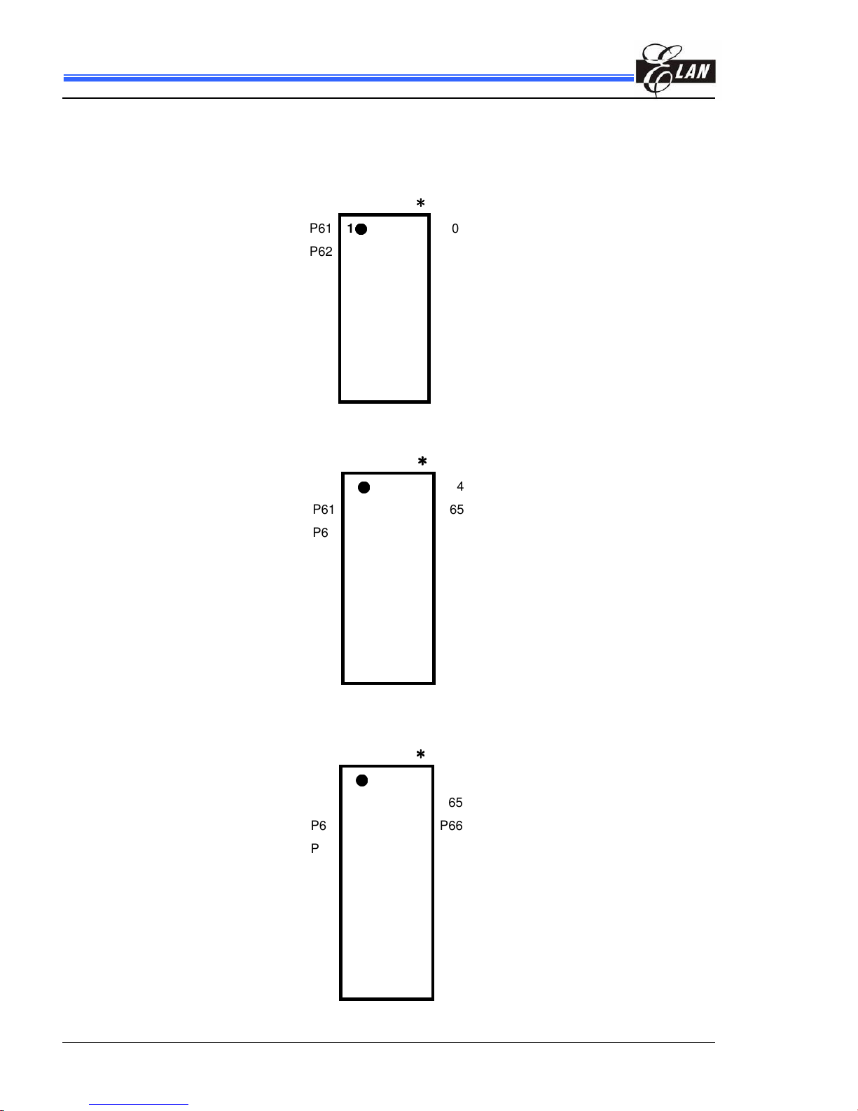
4 Pin Configuration
EM78612A
P61 1
16 P60
P62 2 15 P64
P63 3 14 P65
P70 4 13 P71
P72 5 12 D+/P50
VSS 6 11 D-/P51
V3.3V 7 10
V
DD
OSCI 8 9 OSCO
EM78612B
P60 1
18 P64
P61 2 17 P65
P62 3 16 P66
P63 4 15 P67
P70 5 14 P71
P72 6 13 D+/P50
VSS7 12 D-/P51
V
3.3V
8 11 V
DD
OSCI 9 10 OSCO
EM78612C
P60 1
20 P64
P61 2 19 P65
P62 3 18 P66
P63 4 17 P67
P70 5 16 P71
P72 6 15 P73
NC 7 14 D+/P50
VSS8 13 D-/P51
V
3.3V
9 12 V
DD
OSCI 10 11 OSCO
EM78612
Universal Serial Bus Microcontroller
Product Specification (V1.0) 03.22.2006 •••• 7
(This specification is subject to change without further notice)
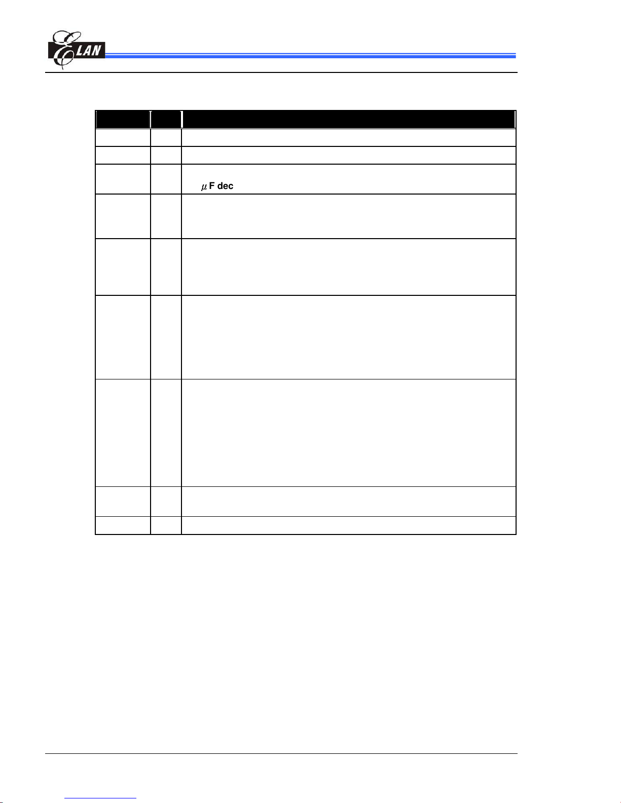
5 Pin Description
Symbol I/O Function
OSCI I 6MHz / 12MHz ceramic resonator input.
OSCO I/O
Return path for 6MHz / 12MHz ceramic resonator.
V
3.3V
O
3.3V DC voltage output from internal regulator. This pin should be tied to a
4.7
F decoupling capacitor to GND.
P60 ~ P67 I/O
Port6 offers up to 8 GIOP pins.
The pull high resistors (132K Ohms) and pull low resistors (10K Ohm) are
selected through pin programming.
P70 ~ P73 I/O
Port7 offers up to 4 GIOP pins. The sink current of P70 & P71 are programmable
for driving LED.
Each pin has pull high resistors (132K Ohm) that can be selected through pin
programming.
D+ / P50 I/O
USB Plus data line interface or PS/2 line interface are user-defined through
firmware setting.
When the EM78612 is running under PS/2 mode, this pin will have an internal
pulled-high resistor (2.2K Ohm), with VDD=5.0V.
When this pin is used as a PS/2 line interface, it will generate an interrupt when
its state changes (Port5 state change interrupt enable).
D- / P51 I/O
USB Minus data line interface or PS/2 line interface are user-defined through
firmware setting.
When the EM78612 is running under PS/2 mode, this pin will have an internal
pulled-high resistor (2.2K Ohm), with VDD=5.0V.
When this pin is used as a PS/2 line interface, it will generate an interrupt when
its state changes (Port5 state change interrupt enable).
When the EM78612 is running under USB mode, this pin will have an internal
pulled-high resistor, 1.5k Ohm, with V
3.3
=3.3V.
V
DD
-
Connects to the USB power source or to a nominal 5V-power supply. Actual V
DD
range can vary between 4.4V and 5.2V.
V
SS
-
Connects to ground.
Table 5-1 Pin Descriptions
EM78612
Universal Serial Bus Microcontroller
8 •••• Product Specification(V1.0) 03.22.2006
(This specification is subject to change without further notice)
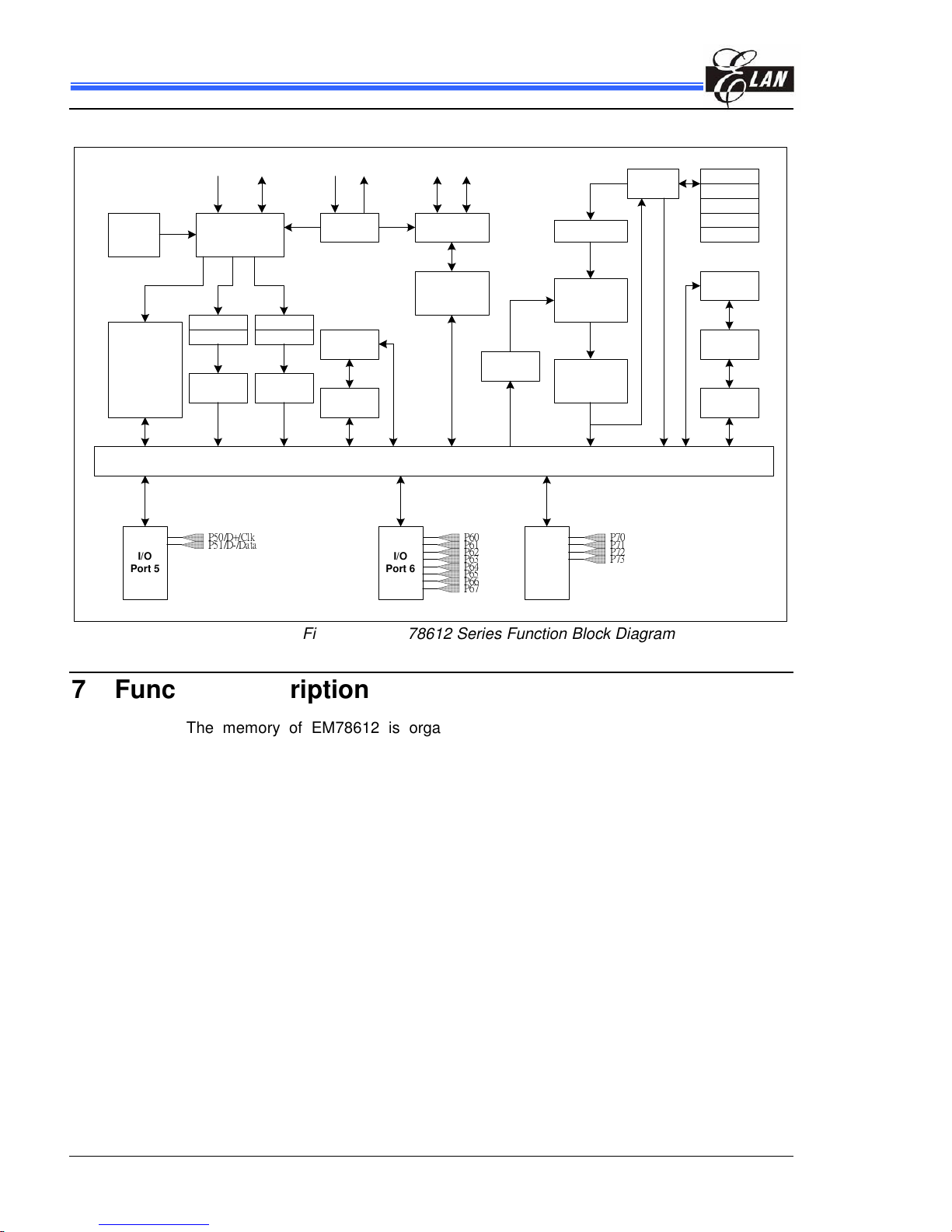
6 Function Block Diagram
Oscillator
Timing
Control
Built-in
RC
Prescaler
R1
(TCC)
WDT
Timer
DATA & CONTROL BUS
OSCI OSCO
R2
(PC)
Stack1
ALU
ACC
R3
(Status)
ROM
Instruction
register
Instruction
Decoder
Interrupt
Control
Reset &
Sleep &
Wake up
Control
3.3V
Regulator
USB
Device
Controller
VDD V3.3
Transceiver
D+ D-
TCCWDT
RAM
R4
(RSR)
Stack2
Stack3
Stack4
Stack5
Prescaler
I/O
Port 7
I/O
Port 6
I/O
Port 5
Figure 6-1 EM78612 Series Function Block Diagram
7 Function Description
The memory of EM78612 is organized into four spaces, namely; User Program
Memory in 2048*13 bits MASK ROM space, Data Memory in 80 bytes SRAM space,
and USB Application FIFOs (for EndPoint0 and EndPoint1). Furthermore, several
registers are used for special purposes.
7.1 Program Memory
The program space of the EM78612 is 2K words, and is divided into two pages. Each
page has 1K words long. After Reset, the 12-bit Program Counter (PC) points to
location zero of the program space.
It has two interrupt vectors, i.e., Interrupt Vectors at 0x0001 and USB Application
Interrupt Vectors at 0x000A. The Interrupt Vector applies to TCC Interrupt, and Port 5
State Changed Interrupt. The USB Application Interrupt Vector is for USB EndPoint
Zero Interrupt, USB Suspend Interrupt, USB Reset interrupt, and USB Host Resume
Interrupt.
After an interrupt, the MCU will fetch the next instruction from the corresponding
address as illustrated in the following diagram.

EM78612
Universal Serial Bus Microcontroller
Product Specification (V1.0) 03.22.2006 •••• 9
(This specification is subject to change without further notice)
After reset Address
0x0000
Reset Vector
0x0001
Interrupt Vector
0x000A
USB Application Interrupt Vector
0x03FF
Page 0
0x0400
0x07FF
Page 1
7.2 Data Memory
The Data Memory has 80 bytes SRAM space. It is also equipped with USB Application
FIFO space for USB Application. The Figure 7-1 (next page) shows the organization of
the Data Memory Space.
7.2.1 Special Purpose Registers
When the micro-controller executes the instruction, specific registers are invoked for
assistance, such as; Status Register which records the calculation status, Port I/O
Control Registers which control the I/O pins’ direction, etc. The EM78612 series
provides a lot more of other special purpose registers with different functions.
There are 15 Special Operation Registers which are located from Address 0x00 to 0x0F.
On other hand, 10 more Special Control Registers are available to control functions or
I/O direction. These are arranged from Address 0x05 to 0x0F.
Note
that Special Control Registers can only be read or written by two instructions; IOR and
IOW.
Program Counter
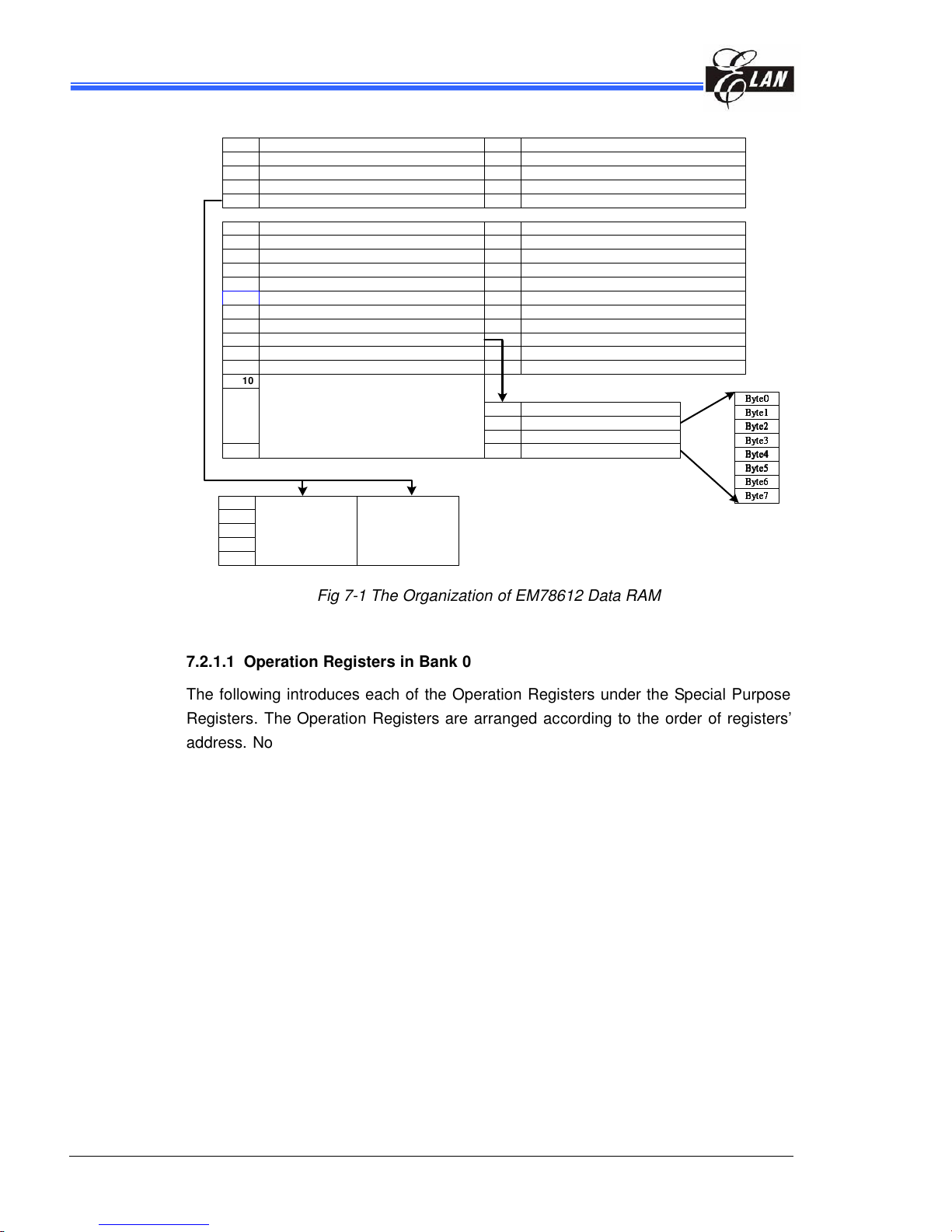
EM78612
Universal Serial Bus Microcontroller
10 •••• Product Specification(V1.0) 03.22.2006
(This specification is subject to change without further notice)
R0 (Indirec tion Add ress ing Registe r)
R1 (Tim e Clock / Counter Register)
R2 (Progra m Counter) & Sta ck
R3 (Status Regist er)
R4 (RAM Sele ct Registe r)
R5 (Da ta lin e I/O Regis ter)
R6 (Port 6 I/O Registe r)
R7 (Port 7 I/O Registe r)
R8 (Port6 w akeup pin selec tion Regis ter)
R9 (Port7 w akeup pin selec tion Regis ter)
RC (US B Applic ation Sta tus Regist er)
RD (US B Applic ation FIFO add ress regis ter)
RE (US B Application FIFO data register)
RF (Int errupt Stat us Register)
00
01
02
03
04
05
06
07
08
Gene ral Purpose Register
09
0C
0D
0F
0E
IOC5 (Port 5 I/O Control Re gister)
IOC6 (Port 6 I/O Control Re gister)
IOC7 (Port 7 I/O Control Re gister)
IOC8 (Sink Cure nt Control Regis ter)
IOCA (O pera tion mode Control Registe r)
IOCB (Port 6 pu ll low Con trol Register)
IOCC (Port 6 pu ll hig h Control Register)
IOCD (Port 7 pu ll hig h Control Register)
IOCE (Special F unction Co ntrol Register)
IOCF (Inter rupt Mask Register)
EP0's FIFO
EP1's FIFO
Data Byte Po inter of EP0
00
01
10
1F
20
General Pu rpos e
Regist ers
(Bank0)
General Pu rpos e
Regist ers
(Bank1)
3F
Data Byte Po inter of EP111
! "$#
! "$#! "$#
! "$#
! "%
! "%! "%
! "%
! "!&
! "!&! "!&
! "!&
! "!'
! "!'! "!'
! "!'
! "(
! "(! "(
! "(
! "!)
! "!)! "!)
! "!)
! "!*
! "!*! "!*
! "!*
! "$+
! "$+! "$+
! "$+
10
Fig 7-1 The Organization of EM78612 Data RAM
7.2.1.1 Operation Registers in Bank 0
The following introduces each of the Operation Registers under the Special Purpose
Registers. The Operation Registers are arranged according to the order of registers’
address. Note that some registers are read only, while others are both readable and
writable.
R0 (Indirect Address Register) Default Value: (0B_0000_0000)
R0 is not a physically implemented register. Its major function is to be an indirect
address pointer. Any instruction using R0 as a pointer actually accesses the data
pointed by the RAM Select Register (R4).
R1 (Time / Clock Counter) Default Value: (0B_0000_0000)
This register TCC, is an 8-bit timer or counter. It is readable and writable as any other
register. The Timer module will increment every instruction cycle . The user can work
around this by writing an adjusted value. The Timer interrupt is generated when the R1
register overflows from FFh to 00h. This overflow sets bit TCIF(RF[0]). The interrupt
can be masked by clearing bit TCIE (IOCF[0]).After Power-on reset and WatchDog
reset, the initial value of this register is 0x00.
 Loading...