ELAN HM9270C, HM9270D, HM9270DM Datasheet

DTMF RECEIVER
HM 9270C/D
- 1 -
General Description
The HM 9270C/D is a complete DTMF receiver integrating both the bandsplit filter and digital decoder
functions. The filter section uses switched capacitor techniques for high- and low-group filters and dial-tone
rejection. Digital counting techniques are employed in the decoder to detect and decode all 16 DTMF tonepairs into a 4-bit code. External component count is minimized by on-chip provision of a differential input
amplifier, clock-oscillator and latched 3-state bus interface.
Features
• Complete receiver in an 18-pin package.
• Excellent performance.
• CMOS, single 5 volt operation.
• Minimum board area.
• Central office quality.
• Low power consumption.
• Power-Down mode (HM9270D only).
• Inhibit-mode (HM9270D only).
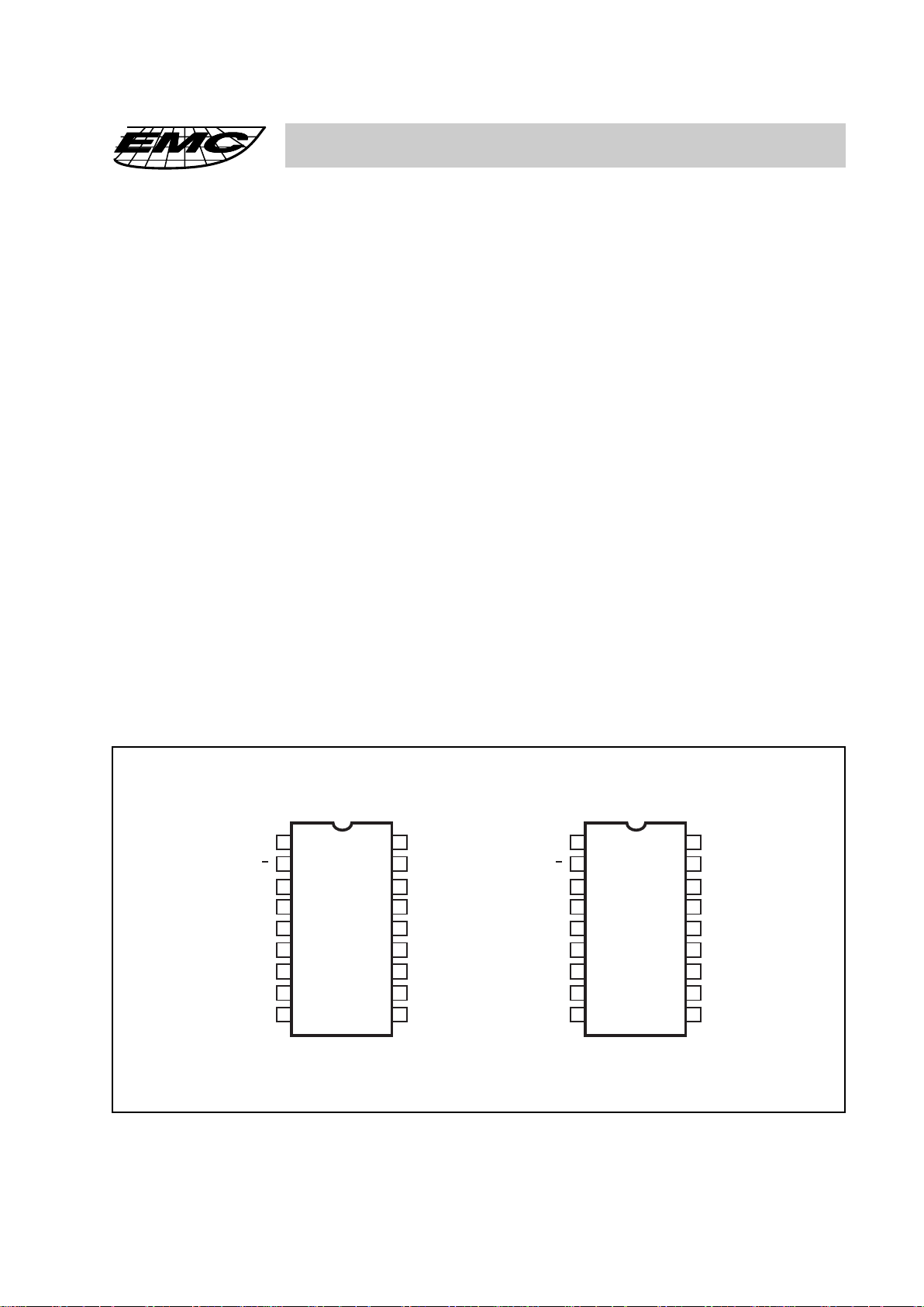
Pin Configurations
* Connect to V
SS
HM9270C
IN+
IN
GS
IC*
IC*
OSC1
OSC2
V
DD
V
REF
ESt
StD
Q4
Q3
Q2
Q1
TOE
St/GT
V
SS
1
2
3
4
5
6
7
8
9
18
17
16
15
14
13
12
11
10
HM9270D
IN+
IN
GS
INH
PWDN
OSC1
OSC2
V
DD
V
REF
ESt
StD
Q4
Q3
Q2
Q1
TOE
St/GT
V
SS
1
2
3
4
5
6
7
8
9
18
17
16
15
14
13
12
11
10

DTMF RECEIVER
HM 9270C/D
- 2 -
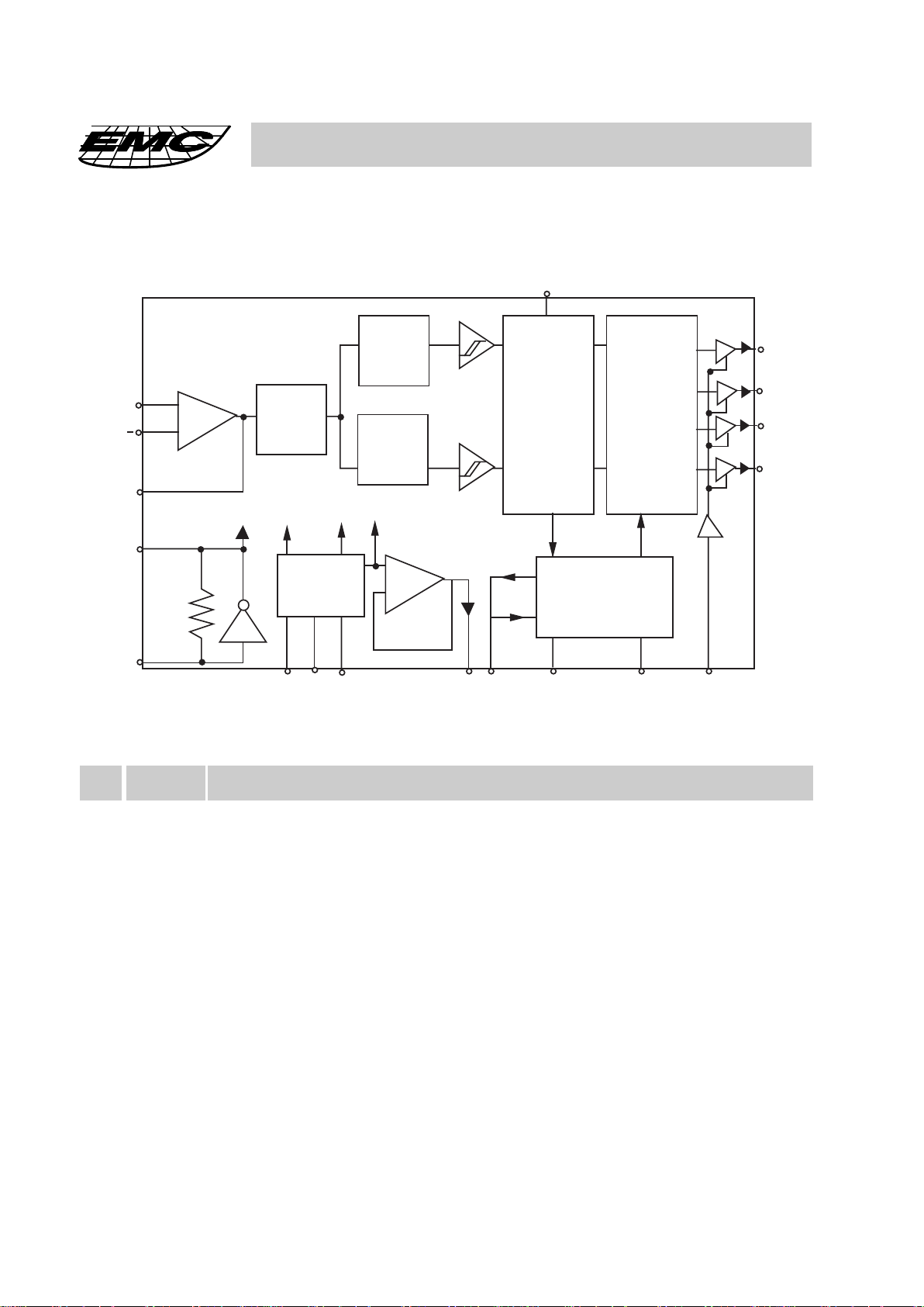
Block Diagram (Figure 1)
Pin Sym.
1 IN+
2 IN-
3GS
4V
REF
5 INH
6 PWDN
7 OSC1
8 OSC2
9V
SS
10 TOE
Non-Inverting input
Invering Input
Gain select. Gives access to output of front-end differential amplifier for connection of
feedback resistor.
Reference voltage output,nominally VDD/2. May be used to bias the inputs at midrail (see
application diagram).
Inhibit (input) logic high inhibit the detection of 1633Hz internal built-in pull down resistor.
(HM9270D only).
Power down (input). Active high power down the device and inhibit the oscillator internal
built-in pull down resistor. (HM9270D only).
Clock Input Clock
Output
Negative power supply, normally connected to 0V.
3-state data output enable (input). Logic high enables the outputs Q1-Q4. Internal pull-up.
Connections to the front-end differential amplifier.
Function
Pin Description
3.579545 MHz crystal connected between these pins completes
internal oscillator.
Q1
Q2
Q3
Q4
OSC1
OSC2
GS
IN
IN+
+
-
CHIP
CLOCKS
CHIP
POWER
CHIP
BIAS
CHIP
REF
DIAL
TONE
FILTER
HIGH
GROUP
FILTER
LOW
GROUP
FILTER
BIAS
CIRCUIT
+
-
ZERO
CROSSING
DETECTORS
DIGITAL
DETECTION
ALGORITHM
CODE
CONVERTER
AND
LATCH
STEERING
LOGIC
TOE
StDVDDV
SS
V
REF
St/
GT
ESt
INH
PWDN

DTMF RECEIVER
HM 9270C/D
- 3 -
Pin Sym.
Function
11 Q1
12 Q2
13 Q3
14 Q4
15 StD
16 ESt
17 St/GT
18 V
DD
3-state data outputs. When enabled by TOE, provide the code corresponding to the last valid
tone-pair received (see code table).
Delayed steering output. Presents a logic high when a received tone-pair has been registered
and the output latch updated; returns to logic low when the voltage on St/GT falls below
V
TSt
.
Early steering output. Presents a logic high immediately when the digital algorithm detects a
recognizable tone-pair (signal condition). Any momentary loss of signal condition will cause
ESt to return to a logic low.
Steering input/guard time output (bi-directional). A voltage greater than V
TSt
detected at St
causes the device to register the detected tone-pair and update the output latch. A voltage
less than V
TSt
frees the device to accept a new tone-pair. The GT output acts to reset the
external steering time-constant; its state is a function of ESt and the voltage on St (see truth
table).
Positive power supply, +5Volts.
DC Electrical Characteristics
Parameter Description
SUPPLY:
V
DD
Operating Supply Voltage
I
cc
Operating Supply Current
P
o
Power Consumption
I
S
Standby Current
INPUTS:
V
IL
Low Level Input Voltage
V
IH
High Level Input Voltage
IIH/I
IL
Input Leakage Current
I
so
Pull Up (Source) Current
R
IN
Input Signal
Impedance Inputs 1,2
V
TSt
Steering Threshold Voltage
Test Conditions Min. Typ. Max. Units
4.75 5.25 V
3.0 7 mA
f=3.579MHz; VDD=5V 15 35 mW
PWDN pin = V
DD
- - 100 µA
1.5 V
3.5 V
VIN=Vss or V
DD
0.1 uA
TOE (Pin 10)=OV 7.5 15 uA
@ 1kHz 10 MΩ
2.35 V
Parameters Min. Max. Units
Power Supply Voltage, VDD - V
SS
6V
Voltage on any pin VSS - 0.3 VDD+ 0.3 V
Current at any pin 10 mA
Operating temperature -40 +85
o
C
Storage temperature -65 +150
o
C
Package power dissipation 500 mW
Note 1. Absolute maximum ratings are those values beyond which damage to the device may
occur.
2. Unless otherwise specified, all voltages are referenced to ground.
3. Power dissipation temperature derating: -12 mV/oC from 65oC to 85oC
Absolute Maximum Ratings (Notes 1, 2 and 3)
 Loading...