

Elan eSL Series, eSLS Series, SLZ000 eSL032 eSL128 eSL256 eSL512 eSL032 A/B, eSL128 A/B, eSL256 A/B User Manual
...
eSL/eSLS Series
(+ eSLZ000)
16 Bits DSP
16 Bits DSP16 Bits DSP
16 Bits DSP
Sound Processor
Sound ProcessorSound Processor
Sound Processor
USER’S MANUAL
ELAN
MICROELECTRONICS CORP.
December 2009
Doc. Version
1.7

Trademark Acknowledgments:
IBM is a registered trademark and PS/2 is a trademark of IBM
Windows is a trademark of Microsoft Corporation
ELAN and ELAN logo
are trademarks of ELAN Microelectronics Corporation
Copyright
© 2006 ~ 2009 by ELAN Microelectronics Corporation
All Rights Reserved
Printed in Taiwan
The contents of this User’s Manual (publication) are subject to change without further notice. ELAN
Microelectronics assumes no responsibility concerning the accuracy, adequacy, or completeness of this
publication. ELAN Microelectronics makes no commitment to update, or to keep current the information and
material contained in this publication. Such information and material may change to conform to each confirmed
order.
In no event shall ELAN Microelectronics be made responsible for any claims attributed to errors, omissions, or
other inaccuracies in the information or material contained in this publication. ELAN Microelectronics shall not
be liable for direct, indirect, special incidental, or consequential damages arising from the use of such information
or material.
The software (if any) described in this publication is furnished under a license or nondisclosure agreement, and
may be used or copied only in accordance with the terms of such agreement.
ELAN Microelectronics products are not intended for use in life support appliances, devices, or systems. Use of
ELAN Microelectronics product in such applications is not supported and is prohibited.
NO PART OF THIS PUBLICATION MAY BE REPRODUCED OR TRANSMITTED IN ANY FORM OR BY
ANY MEANS WITHOUT THE EXPRESSED WRITTEN PERMISSION OF ELAN MICROELECTRONICS.
ELAN MICROELECTRONICS CORPORATION
Headquarters:
No. 12, Innovation Road 1
Hsinchu Science Park
Hsinchu, Taiwan 30077
Tel: +886 3 563-9977
Fax: +886 3 563-9966
http://www.emc.com.tw
Hong Kong:
Elan (HK) Microelectronics
Corporation, Ltd.
Flat A, 19/F, World Tech Centre
95 How Ming Street, Kwun Tong
Kowloon , HONG KONG
Tel: +852 2723-3376
Fax: +852 2723-7780
elanhk@emc.com.hk
USA:
Elan Information
Technology Group (USA)
1821 Saratoga Ave., Suite 250
Saratoga, CA 95070
USA
Tel: +1 408 366-8225
Fax: +1 408 366-8220
Shenzhen:
Elan Microelectronics
Shenzhen, Ltd.
3F, SSMEC Bldg., Gaoxin S. Ave.
I
Shenzhen Hi-tech Industrial Park
(South Area), Shenzhen, CHINA
Tel: +86 755 2601-0565
Fax: +86 755 2601-0500
Shanghai:
Elan Microelectronics
Shanghai, Ltd.
23/Bldg. #115 Lane 572, Bibo Road
Zhangjiang Hi-Tech Park
Shanghai, CHINA
Tel: +86 21 5080-3866
Fax: +86 21 5080-4600

Contents
eSL/eSLS Series (+ eSLZ000) User’s Manual Contents •••• iii
Contents
Contents
ContentsContents
Contents iii
iiiiii
iii
Chapter 1
Chapter 1Chapter 1
Chapter 1 1111
Introduction
IntroductionIntroduction
Introduction 1111
1.1 Introduction to eSL/eSLS Series and eSLZ000 ICs...................................................1
1.2 Features ..................................................................................................................... 2
1.3 Parts List and Properties ............................................................................................3
1.3.1 eSLZ000 and eSL ICs Parts List and Properties............................................. 3
1.3.2 eSLS ICs Parts List and Properties ..................................................................4
1.3.3 Properties Comparison between eSLZ000, eSL, and eSLS ICs .....................5
1.4 Algorithm Selection Table .........................................................................................6
1.4.1 eSLZ000 and eSL ICs Parts List and Properties............................................. 6
1.4.2 eSLS ICs Parts List and Properties ..................................................................8
1.5 Typical Applications..................................................................................................9
1.6 Pin Descriptions ...................................................................................................... 10
1.6.1 Power Supply ................................................................................................ 10
1.6.2 System Control.............................................................................................. 11
1.6.3 DAC Output .................................................................................................. 11
1.6.4 Two Stage Amplifier & Touch Pad Positioning (Supports eSL and eSLZ000
ICs only)................................................................................................................... 11
1.6.5 I/O Port..........................................................................................................12
1.6.6 Data ROM Interface (eSLZ000 only) ...........................................................14
1.6.7 ICE Interface (eSLZ000 only) ...................................................................... 14
Chapter 2
Chapter 2Chapter 2
Chapter 2 17
1717
17
Architecture
ArchitectureArchitecture
Architecture 17
1717
17
2.1 eSL System Block Diagram.................................................................................... 17
2.2 Program ROM and Data RAM Description............................................................18
2.2.1 Program ROM/RAM.......................................................................................18
2.2.2 Data RAM and Bank Select Register.............................................................. 19
2.3 Addressing Modes....................................................................................................20
2.3.1 Register Direct Addressing ...........................................................................20
2.3.2 Register Indirect Addressing......................................................................... 20

Contents
iv •••• Contents eSL/eSLS Series (+ eSLZ000) User’s Manual
2.3.3 Indirect Addressing with Post-Decrement ....................................................21
2.3.4 Indirect Addressing with Post-Increment......................................................21
2.3.5 I/O Direct Addressing ...................................................................................21
2.3.6 RAM (Data) Direct Addressing ....................................................................22
2.3.7 Immediate Addressing ..................................................................................23
2.3.8 Relative Program Addressing .......................................................................23
2.3.9 Data Indirect Addressing with Displacement ...............................................24
2.4 Register Architecture................................................................................................25
2.4.1 General Purpose Registers ............................................................................26
2.4.2 Program Counter (PC) ..................................................................................26
2.4.3 Stack Pointer (SP) ......................................................................................... 26
2.4.4 Repeat and Loop Registers ...........................................................................26
2.4.5 Status Register (SR)......................................................................................27
2.5 Instruction Set ..........................................................................................................29
2.5.1 Logic and Mathematic Instructions ..............................................................30
2.5.2 Conditional Branch Instruction.....................................................................31
2.5.3 Shift and Rotation Instructions .....................................................................32
2.5.4 Data Transfer Instruction ..............................................................................33
2.5.5 Bit Operation Instruction ..............................................................................34
2.5.6 Control Instructions ......................................................................................35
2.5.7 DSP Instruction.............................................................................................36
2.6 Power Supply Circuit ...............................................................................................39
2.6.1 Power Supply Attributes and Features ..........................................................39
2.7 Oscillator System ..................................................................................................... 40
2.7.1 Block Diagram ..............................................................................................40
2.7.2 Operation.......................................................................................................41
2.7.3 CPU Control Registers.................................................................................. 44
2.8 Reset System ...........................................................................................................44
2.8.1 Block Diagram ..............................................................................................45
2.8.2 Operation.......................................................................................................46
2.8.3 Power-On Reset (POR).................................................................................47
2.8.4 Brown-Out Reset (BOR)...............................................................................48
2.9 System Mode Operation...........................................................................................49
2.9.1 Block Diagram ..............................................................................................49
2.9.2 Operation.......................................................................................................49
2.9.4 Registers........................................................................................................ 50
2.9.5 System Mode Operation Examples............................................................... 51
2.10 Exception-Handling .................................................................................................51
2.10.1 Reset..............................................................................................................51
2.10.2 Trap Instruction (TRAP)............................................................................... 51
2.10.3 Interrupts .......................................................................................................51
2.11 External Interrupt....................................................................................................57
2.11.1 External Interrupt Control Register..............................................................57

Contents
eSL/eSLS Series (+ eSLZ000) User’s Manual Contents •••• v
2.11.2 Application Examples................................................................................... 58
2.12 Stack Pointer Limit (SPLIM).................................................................................. 59
2.12.1 General Description...................................................................................... 59
2.12.2 Block Diagram .............................................................................................60
2.12.3 Register Description..................................................................................... 61
2.12.4 Operation Description ..................................................................................61
Chapter 3
Chapter 3Chapter 3
Chapter 3 63
6363
63
Peripheral Control
Peripheral ControlPeripheral Control
Peripheral Control 63
6363
63
3.1 Watchdog Timer (WDT) .........................................................................................63
3.1.1 Block Diagram ..............................................................................................64
3.1.2 Watchdog Control Register........................................................................... 64
3.1.3 Examples ........................................................................................................ 65
3.2 Real Time Clock (RTC) ..........................................................................................66
3.2.1 Real Time Clock and Interrupt Block Diagram ............................................ 66
3.2.2 Real Time Clock Control Register ................................................................67
3.2.3 RTC Timing....................................................................................................68
3.2.4 Examples.......................................................................................................70
3.3 Timer .......................................................................................................................71
3.3.1 Timer 0/1....................................................................................................... 71
3.3.2 Timer 2/3....................................................................................................... 74
3.4 Pulse Width Modulation (PWM) ............................................................................. 84
3.4.1 Features .........................................................................................................84
3.4.2 Block Diagram ..............................................................................................85
3.4.3 Operation.......................................................................................................85
3.4.4 Registers........................................................................................................ 87
3.4.5 Examples.......................................................................................................89
3.5 Digital to Analog Converter (DAC) ........................................................................ 90
3.5.1 Features .........................................................................................................90
3.5.2 Operation.......................................................................................................90
3.5.3 Registers........................................................................................................ 90
3.5.4 Application Example ....................................................................................91
3.5.5 Examples.......................................................................................................91
3.6 Analog to Digital Converter (eSL and eSLZ000 only)............................................92
3.6.1 Features .........................................................................................................93
3.6.2 Registers........................................................................................................ 93
3.6.3 Operation.......................................................................................................95
3.6.4 Examples.......................................................................................................97
3.7 Data ROM ..............................................................................................................100
3.7.1 Features .......................................................................................................100

Contents
vi •••• Contents eSL/eSLS Series (+ eSLZ000) User’s Manual
3.7.2 Block Diagram ............................................................................................100
3.7.3 Register Description....................................................................................101
3.7.4 Examples.....................................................................................................102
3.8 Serial Peripheral Interface (eSL and eSLZ000 only).............................................104
3.8.1 Features .......................................................................................................104
3.8.2 Block Diagram ............................................................................................106
3.8.3 Pin Description............................................................................................106
3.8.4 SPI Register ................................................................................................109
3.8.5 SPI Transfer Format .................................................................................... 111
3.8.6 SPI Timing Diagrams.................................................................................. 112
3.8.7 Master Mode Operation .............................................................................. 115
3.8.8 Slave Mode Operation ................................................................................116
3.8.9 SPI Master Initial Flow Chart ..................................................................... 117
3.8.10 SPI Boot Flash (Interface) and SPI Data Flash (Interface) ...................... 117
3.8.11 Examples..................................................................................................... 118
3.9 Microphone Front End (eSL and eSLZ000 only)................................................... 119
3.9.1 Registers...................................................................................................... 119
3.9.2 Examples ..................................................................................................... 122
3.10 I/O Pad Architecture .............................................................................................123
3.10.1 CMOS Pad Cofiguration Diagrams............................................................ 124
3.11 General Purpose Input Output ..............................................................................128
3.11.1 Features.......................................................................................................128
3.11.2 I/O Port Register Descriptions ...................................................................129
3.11.3 Input Mode with Pull Up Resistor Delay Time ..........................................132
3.11.4 I/O Port Application Examples................................................................... 132
3.12 Voltage Regulator 5V / 3V....................................................................................134
Chapter 4
Chapter 4Chapter 4
Chapter 4 137
137137
137
El
ElEl
Electrical Characteristics
ectrical Characteristicsectrical Characteristics
ectrical Characteristics 137
137137
137
4.1 CPU Voltage – Frequency Graph ..........................................................................137
4.2 Absolute Maximum Ratings..................................................................................138
4.2.1 eSL and eSLS.............................................................................................. 138
4.2.2 eSLZ000...................................................................................................... 138
4.3 DC Characteristics ................................................................................................139
4.3.1 For eSL, eSLS and eSLZ000 ...................................................................... 139
4.3.2 For eSL and eSLS Only ..............................................................................140
4.3.3 For eSLZ000 Only ......................................................................................141
Chapter 5
Chapter 5Chapter 5
Chapter 5 143
143143
143

Contents
eSL/eSLS Series (+ eSLZ000) User’s Manual Contents •••• vii
Application Circuits
Application CircuitsApplication Circuits
Application Circuits 143
143143
143
5.1 eSL Application Circuit ..........................................................................................143
5.2 eSLS Application Circuit ........................................................................................144
5.3 eSLZ000 Application Circuit..................................................................................145
Chapter 6
Chapter 6Chapter 6
Chapter 6 147
147147
147
Instruction Set Summary
Instruction Set SummaryInstruction Set Summary
Instruction Set Summary 147
147147
147
6.1 Symbol Summary.................................................................................................. 147
6.1.1 General Symbol ..........................................................................................147
6.1.2 Operand.......................................................................................................147
6.1.3 Operator ......................................................................................................148
6.1.4 Flag status (SR)...........................................................................................148
6.1.4 Operation Explainations..............................................................................148
6.2 Instruction Set Tables............................................................................................ 149
6.2.1 Data Transfer Instructions........................................................................... 149
6.2.2 Arithmetic Operation Instructions ..............................................................150
6.2.3 Logic Operation Instructions ......................................................................152
6.2.4 Bit Operation Instructions
*
.........................................................................153
6.2.5 Program Jump Instructions ......................................................................... 154
Appendix
AppendixAppendix
Appendix 157
157157
157
eSL and eSLZ000 Special Function Registers
eSL and eSLZ000 Special Function RegisterseSL and eSLZ000 Special Function Registers
eSL and eSLZ000 Special Function Registers 157
157157
157
A.1 List of eSL & eSLZ000 Special Function Registers ..............................................157
A.2 List of eSLS Special Function Registers...............................................................159
Appendix
AppendixAppendix
Appendix 161
161161
161
Flash Memory Compatibility List
Flash Memory Compatibility ListFlash Memory Compatibility List
Flash Memory Compatibility List 161
161161
161
A.1 List of eSL & eSLZ000 Flash Memory Compatibility .......................................... 161

Contents
viii •••• Contents eSL/eSLS Series (+ eSLZ000) User’s Manual

Contents
eSL/eSLS Series (+ eSLZ000) User’s Manual Contents •••• ix
User’s Manual Revision History
Doc. Version
Revision Description Date
1.0
Official Version Release with following changes:
• Revised ADC Timing Diagram in Section 3.6.3
• Revised MOV description in Section 4.5.2
• Add clock system description in Section 2.5
• Add interrupt description in Section 2.8.3
• Revised SPI description in Section 3.4
• Revised Opening Temperature Range in Section 4.1.2
2006/12/11
1.1
Revised Appliation circuits in Section 4.2.2
Add comment in Section 4.3.2
Modified OSCO in Section 2.7.2.1
Add comment in Selection table in Section 1.3.1
Modified Boot SPI in Section 1.3.3
Add RTC timing information in Section 3.2
Modified interrupt vector address width in Section 2.10.3
Modified description and figure in Section 2.12
Modified layout hierarchy in Section 4
Modified the Sampleing Rate Range in Section 1.3.1
Added the IOVDD, IOVSS, AVDD, AVSS in Section 1.5.1
2007/03/26
1.2
Modified long MOV instruction description in Section 6.2.1
Modified DROM code example in Section 3.7.4
Added eSL032
Modified SPI transmitter/receiver only in Section 3.8.7 and 3.8.8
Modified the Temperature Range in Section 4.2
Modified the Power supply voltage in Section 4.3.1
Modified the example in Section 3.6.4 and 3.5.5
Modified the IP attributes and definiations in Section 3
Added algorithm support such as beat tracking, sound location,
speech control, pitch control in Section 1.2 and 1.3
Added the note about power optimization in Section 2.9.2 and 3.4.4
Added ADC input resistance and capacitance in Section 3.6
2007/08/10
1.3
Added package information in Section 1.3
Modified PWMP and PWMD initial value in Section 3.4.4
Modified Application Circuit in Section 5
Modified Figure number in Section 3.10
2007/11/10
1.4
SPI serial clock consideration in Section 3.8.3.1 and 3.8.8
Modified PWM current in Section 4.3
Modified BSR description in Section 2.2.2
Modified data direct address mode in Section 2.3.6
Modified mov instruction in Section 2.5.4.1
Added PortC DC characteristic in Section 4.1.3
2008/01/10
1.5
Modify LSA, LEA initlal value in Appendix
Modify Application Circuit diagram in Section 5
Added EXINT wake-up comment in Section 2.11
Added FSR change comment in Section2.7.2
Add Regulator comment in Section 3.12
Added flash memory support table in Appendix
Modified Algorithm support in Section 1.2 and 1.3
2008/10/15

Contents
x •••• Contents eSL/eSLS Series (+ eSLZ000) User’s Manual
Modified Regulator comment in Section 3.12 and Section 5
1.6
Modify WDT example in Section 3.1.3
Modify Definition of TCNT2 and TCNT3 in Appendix A
Added Algorithm-related section in Section 1.4
2009/04/15
1.7
Modify DROM example code in Section 3.7.4
Modify PC[7:0] pull-up resister in Section 4.3.1
Added ADC convertion time in Section 3.6.2
Added ADC enable timing in Section 3.6.2
2009/12/01

Contents
eSL/eSLS Series (+ eSLZ000) User’s Manual Contents •••• xi


Chapter 1
eSL/eSLS Series (+ eSLZ000) User’s Manual Introduction •••• 1
Chapter 1
Introduction
1.1 Introduction to eSL/eSLS Series and eSLZ000 ICs
The eSL/eSLS Series and eSLZ000 ICs (or “eSL Series” for short) differ from
each other in the following manner:
eSL ICs fully comply with all features of the eSL Series.
eSLS ICs is the simplified version of the eSL ICs. Hence, these chips
have simpler performance than the eSL ICs.
eSLZ000 IC is the eSLZ000 ICE kernel chip used to emulate the eSL/eSLS
Series.
ELAN eSL Series ICs are 16-bit DSP Sound Processor with multi-channel
speech and instrument playback based on Elan 16-bit DSP platform. The series
has a powerful 16-bit DSP architecture that handles most of the speech/melody
functions. Speech and melody can be played back simultaneously with the
speech synthesis implemented by software. A wide range of compression bit
rates and various volume levels are supported. eSL Series chips are equipped
with real instrument waveform which enable the chips to obtain good quality
melody. ELAN eSL peripherals include RTC, Timer, WDT, DAC, PWM, etc.
The eSL Series ICs offer FAST, SLEEP, GREEN, and SLOW modes of
operation. The use of GREEN and SLOW mode further reduces power
consumption. Moreover, GREEN mode also provides RTC function for
wake-up propose.
The chips are designed as a cost effective processors offering optimized
performance and are ideal for such applications as high compression rate digital
voice signal, high quality instrument melody, voice recognition, digital sound
effect, etc. The eSL Series constructive features motivate exploration into wide
variety of new creative ideas for more innovative products.
ELAN eSL Series perform extremely well in speech application based on
powerful DSP architecture and are endowed with good algorithm for audio
compression.

Chapter 1
2 •••• Introduction eSL/eSLS Series (+ eSLZ000) User’s Manual
1.2 Features
MCU
• 16-bit RISC CPU architecture
• CPU clock: 20MHz @ 3.3V (eSL and eSLS only)
• CPU clock: 18MHz @ 3.3V (eSLZ000 only)
• Programmable PLL
• 4 CPU operation modes (Fast, Slow, Green, & Sleep)
• Powerful DSP Instruction Set (MAC, DIV, RPT, LOOP)
• Saturation mode supported
• 8 general purpose registers (GPR)
• 20 interrupt sources with 2-level priority (eSL and eSLZ000 only)
• 17 interrupt source with 2-level priority (eSLS only)
Memory
• 32K-word program memory
• 2K-word data RAM (eSL and eSLS only)
• 8K-word data RAM (eSLZ000 only)
• 32/128/256/512K-word data ROM (eSL only)
• 128/256/512K-word data ROM (eSLS only)
• External data ROM up to 32MB (eSLZ000 only)
Peripherals
• Real Time Clock (RTC) with wake up function
• Four 8-bit timers, two general purpose timer, two multiple-function timer
• 8-bit Watch Dog Timer (WDT) with general purpose timer capability
• 40 GPIO + 8 Output (eSL and eSLZ000 only)
• 24 GPIO (eSLS only)
• Serial Peripheral Interface (eSL and eSLZ000 only)
• 12-bit Analog to Digital Converter with touch panel and MIC inputs
(eSL and eSLZ000 only)
• Built-in regulator
• 12-bit current-steering Digital to Analog Converter (DAC)
• 10-bit resolution Pulse Width Modulation (PWM)
Chapter 1
eSL/eSLS Series (+ eSLZ000) User’s Manual Introduction •••• 3
1.3 Parts List and Properties
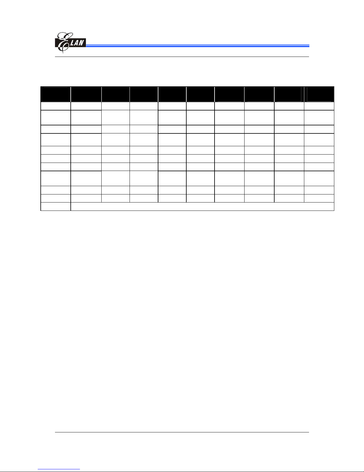
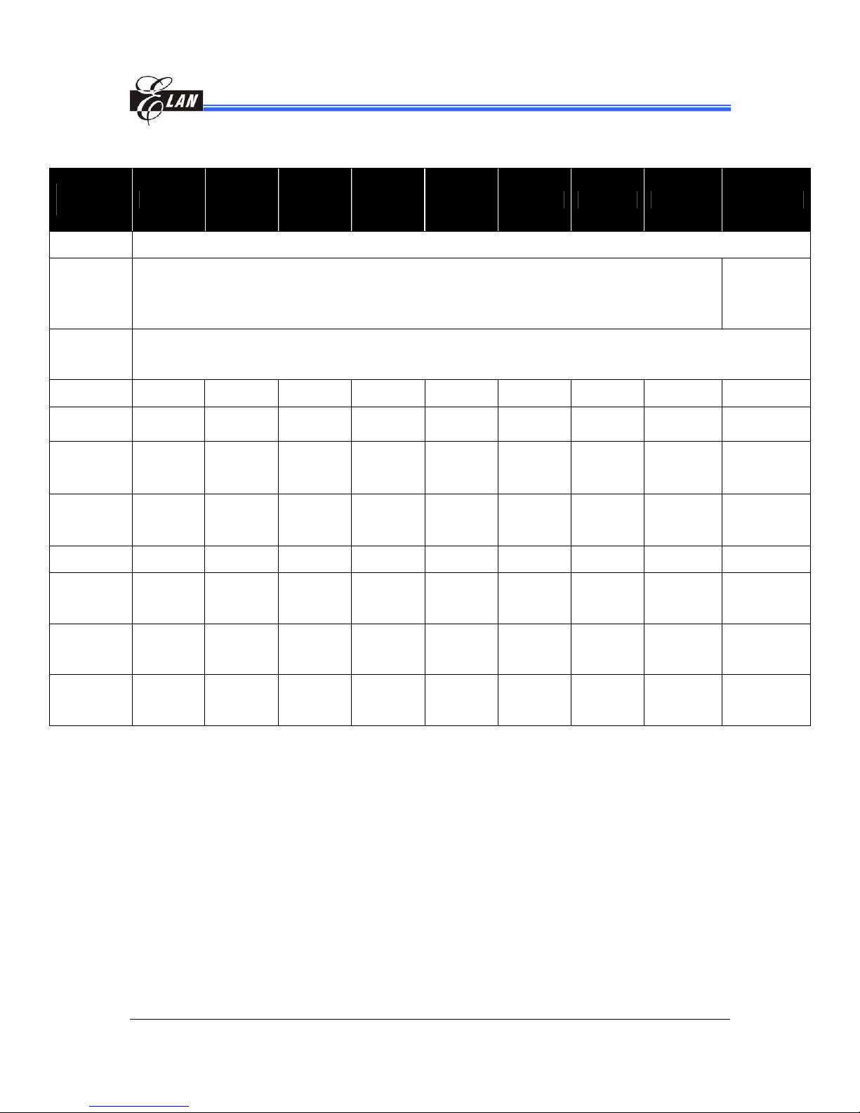
1.3.1 eSLZ000 and eSL ICs Parts List and Properties
Product
No.
eSLZ000 eSL032 eSL128 eSL256 eSL512
eSL032
A/B*
eSL128
A/B*
eSL256
A/B*
eSL512
A/B/C*
Pin Count
138 81 81 81 81 81 81 81 81
Program
ROM
32K *16
(SRAM)
32K*16 32K*16 32K*16 32K*16 32K *16 32K *16 32K *16 32K *16
Data RAM 8K *16 2K *16 2K *16 2K *16 2K *16 2K *16 2K *16 2K *16 2K *16
Data ROM
External
(Up to 16M*16)
32K * 16 128K*16 256K*16 512K*16 32K * 16 128K * 16 256K * 16 512K * 16
Timer 4*8-bit 4*8-bit 4*8-bit 4*8-bit 4*8-bit 4*8-bit 4*8-bit 4*8-bit 4*8-bit
Watch Dog Yes Yes Yes Yes Yes Yes Yes Yes Yes
PWM 10-bit 10-bit 10-bit 10-bit 10-bit 10-bit 10-bit 10-bit 10-bit
Current
D/A
12-bit 12-bit 12-bit 12-bit 12-bit 12-bit 12-bit 12-bit 12-bit
A/D 12-bit 12-bit 12-bit 12-bit 12-bit 12-bit 12-bit 12-bit 12-bit
SPI 1 sets 1 set 1 set 1 set 1 set 1 set 1 set 1 set 1 set
I/O 40 I/O ports + 8 Output ports
*
The product number with an “A,B,C” means the chip supports advanced audio algorithm.
Chapter 1
4 •••• Introduction eSL/eSLS Series (+ eSLZ000) User’s Manual
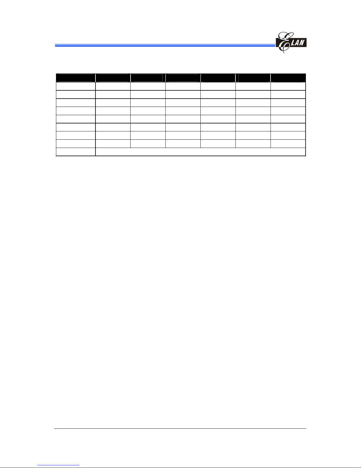
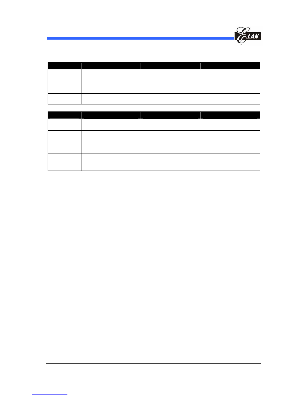
1.3.2 eSLS ICs Parts List and Properties
Product No. eSL128S eSL256S eSL512S
eSL128SA
*
eSL256SA
*
eSL512SA
*
Pin Count 45 45 45 45 45 45
Program ROM 32K *16 32K *16 32K *16 32K *16 32K *16 32K *16
Data RAM 2K *16 2K *16 2K *16 2K *16 2K *16 2K *16
Data ROM 128K * 16 256K * 16 512K * 16 128K * 16 256K * 16 512K * 16
Timer 4*8-bit 4*8-bit 4*8-bit 4*8-bit 4*8-bit 4*8-bit
Watch Dog Yes Yes Yes Yes Yes Yes
PWM 10-bit 10-bit 10-bit 10-bit 10-bit 10-bit
Current D/A 12-bit 12-bit 12-bit 12-bit 12-bit 12-bit
I/O 24 I/O ports
*
The product number with an “A” means the chip supports advanced audio algorithm.
Chapter 1
eSL/eSLS Series (+ eSLZ000) User’s Manual Introduction •••• 5
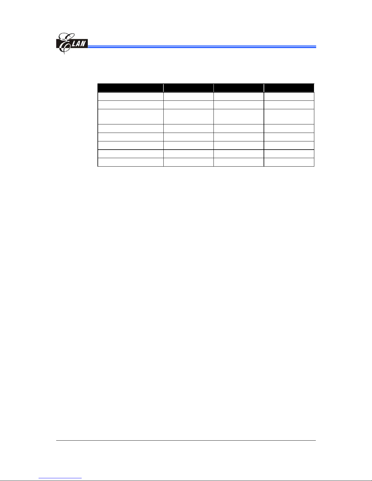
1.3.3 Properties Comparison between eSLZ000, eSL,
and eSLS ICs
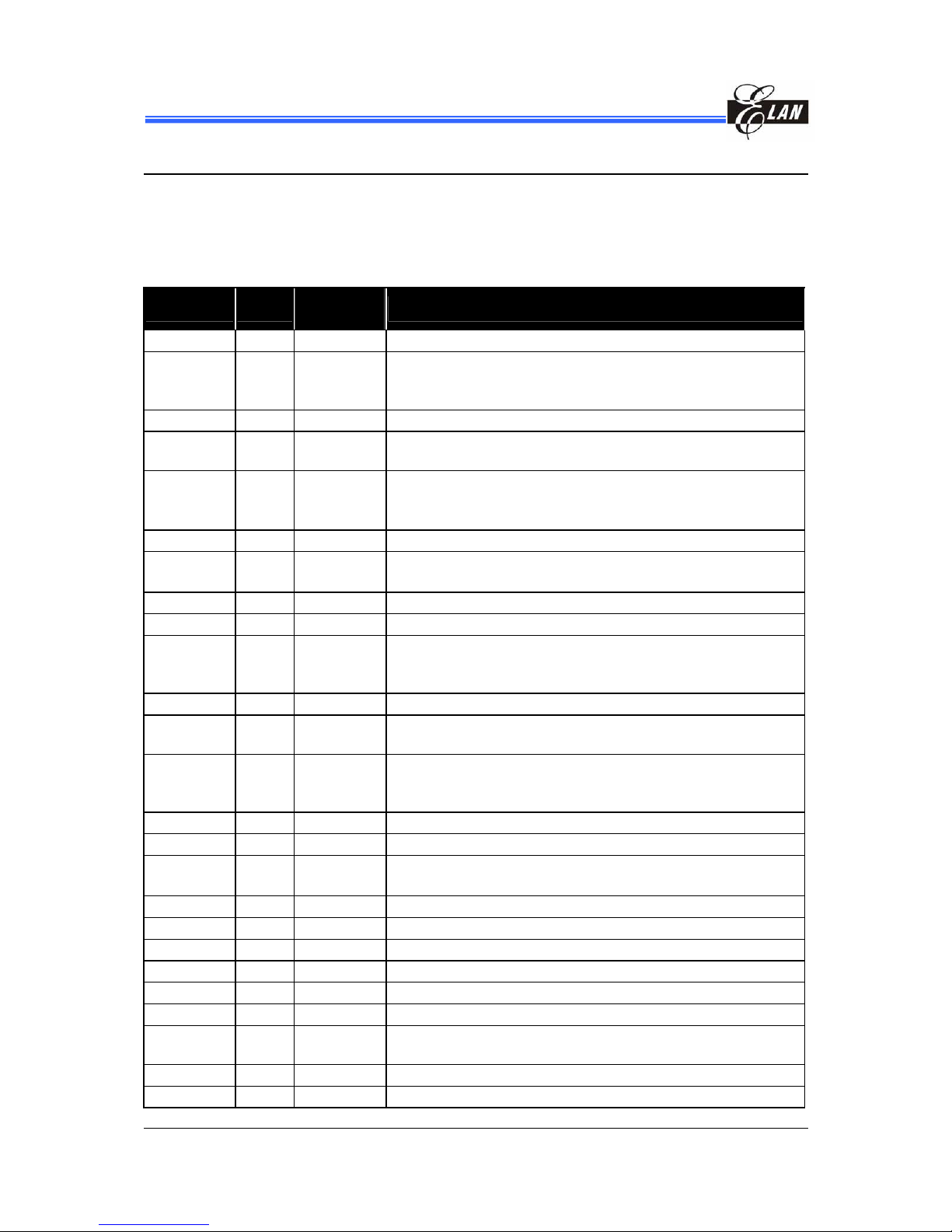
Product No. eSLZ000 eSL eSLS
JTAG ICE Yes No No
Boot SPI Yes No No
Total I/O number 48 48
24
(PortA + PortB0~7)
Large Current I/O number
8+4 8+4 4 (PortA 12~15)
Wake Up Pin 16+5 16+5 8+4
SPI Yes Yes No
MIC Front-end AGC Yes Yes No
ADC Yes Yes No
Chapter 1
6 •••• Introduction eSL/eSLS Series (+ eSLZ000) User’s Manual
1.4 Algorithm Selection Table
The ELAN eSL Series algorithm feature
• Built-in software voice synthesizer (0.8K ~ 96Kbps@8kHz)
• Multiple flash with volume level option
• Control port output value directly by waveform (waveform control port)
• Support mark number in waveform with ROM optimized configuation
• Up to 2-channel speech with different channel sample rate or 1-channel
speech + 8-channel melody
• Voice recording in 12, 16, 20, and 32 Kbps@8KHz
• Support beat tracking function to detect music tempo
• Support speed control to adjust playback speed
• Support pitch control to change voice pitch
• Support sound source detection function to detect the angle of sound
position
• Support speaker dependent recognition to recognize voice command &
control function which is dependent on speaker
• Support speaker independent recognition to recognize voice command &
control function which is independent on speaker
• Support handwriting recognition engine to recognize characters, numeral,
symbols, and gestures.
1.4.1 eSLZ000 and eSL ICs Parts List and Properties
Product No. eSL032 eSL128 eSL256 eSL512
Audio**
Up to 2-channel speech with different channel sample rate or
1-channel speech + 8-channel melody
Coding Type** 12K/16K/20K/32K/40K/48K/96K bps @ 8KHz
Sampling Rate
Range
**
6kHz ~ 48KHz
Recording Yes
Chapter 1
eSL/eSLS Series (+ eSLZ000) User’s Manual Introduction •••• 7
Product
No.
eSL032A* eSL128A* eSL256A* eSL512A* eSL032B* eSL128B* eSL256B* eSL512B* eSL512C*
Audio** Up to 2-channel speech with different channel sample rate or 1-channel speech + 8-channel melody
Coding
Type**
0.8K~96K bps @ 8KHz
12K/16K/20K
/32K/40K
/48K/96K bps
@8KHz
Sampling
Rate
Range**
6kHz ~ 48KHz
Recording Yes Yes Yes Yes Yes Yes Yes Yes No
Beat
Tracking
Yes Yes Yes Yes Yes Yes Yes Yes No
Speaker
Independent
Recognition
No No No No Yes Yes Yes Yes No
Speaker
Dependent
Recognition
No No No No Yes Yes Yes Yes No
Recording Yes Yes Yes Yes Yes Yes Yes Yes No
Sound
Source
Detection
Yes Yes Yes Yes Yes Yes Yes Yes No
Speech
Speed/Pitch
Control
Yes Yes Yes Yes Yes Yes Yes Yes Yes
Hand
Writing
Recognition
No No No No No No No No Yes
Chapter 1
8 •••• Introduction eSL/eSLS Series (+ eSLZ000) User’s Manual
1.4.2 eSLS ICs Parts List and Properties
Product No.
eSL128S eSL256S eSL512S
Audio**
UP to 2-channel speech with different channel sample rate or 1-channel speech + 8-channel
melody
Coding
Type**
12K/16K/20K/24K/32K/40K/96K bps @8KHz
Sampling Rate
Range**
6KHz ~ 48KHz
Product No.
eSL128SA* eSL256SA* eSL512SA*
Audio**
UP to 2-channel speech with different channel sample rate or 1-channel speech + 8-channel
melody
Coding
Type**
0.8K~96K bps @8kHz
Sampling Rate
Range**
6KHz ~ 48KHz
Speech
Speed/Pitch
Control
Yes
*
The product number with an “A,B,C” means the chip supports advanced algorithm. A series support vocal high
compress application. B series support vocie recognition (SI/SD) application, C series support hand write
recognition (HWR) application.
**
For further details, refer to the pertinent eSL Series Assembler Reference Guide, eSL Series C Macro
Reference Guide and related Application note.

Chapter 1
eSL/eSLS Series (+ eSLZ000) User’s Manual Introduction •••• 9
1.5 Typical Applications
Long Duration Speech and Melody Playback
Voice Recognition
Education Learning Products
Recording and Playback Products
Intelligent Interactive Talking Toys
Caller ID (DTMF/FSK decoder)
Power Conversion and Motor Control
General Purpose Controller
Chapter 1
10 •••• Introduction eSL/eSLS Series (+ eSLZ000) User’s Manual
1.6 Pin Descriptions
1.6.1 Power Supply
Refer to Section 2.6, Power Supply Circuit for more detailed information.
Name Type
Supported
Voltage
Description
VDD_CPU P 3V Positive power supply for CPU, digital peripheral and DRAM
VDD_PM P 3V
Positive power supply for PROM, DROM and POR (eSL and eSLS
only)
Positive power supply for PRAM and POR (eSLZ000 only)
VDD_OSC P 3V Positive power supply for Oscillator system and PLL
VDD_ICE P 3V
Positive power supply for DROM, ICE function and boot function I/O
pad (eSLZ000 only)
IOVDD_PWM P 3V, 5V
Positive power supply for PortD and PWM I/O pad
(eSL and eSLZ000 only)
Positive power supply for PWM I/O pad(eSLS Seies only)
IOVDD_PB P 3V, 5V Positive power supply for PortA.2~15 and PortB I/O pad
IOVDD_PC P 3V, 5V
Positive power supply for PortC I/O pad
(eSL Series and eSLZ000)
IOVDD* P 3V, 5V Positive power supply (eSLS Series only)
VSS_CPU P 0V Negative power supply for CPU, digital peripheral and DRAM
VSS_PM P 0V
Negative power supply for PROM, DROM and POR (eSL and eSLS
only)
Negative power supply for PRAM and POR (eSLZ000 only)
VSS_OSC P 0V Negative power supply for Oscillator system and PLL
VSS_ICE P 0V
Negative power supply for DROM, ICE function and boot function I/O
pad (eSLZ000)
IOVSS_PWM P 0V
Negative power supply for PortD and PWM I/O pad (eSL and eSLZ000
only)
Negative power supply for PWM I/O pad (eSLS only)
IOVSS_PB P 0V Negative power supply for PortA.2~15 and PortB I/O pad
IOVSS* P 0V Negative power supply (eSLS Series only)
IOVSS_PC P 0V
Negative power supply for PortC I/O pad
(eSL and eSLZ000 only)
AVDD_AD P 3V Positive power supply for A/D (eSL and eSLZ000 only)
AVDD_DA P 3V Positive power supply for D/A
AVDD** P 3V Positive power supply (eSLS Series only)
AVSS_AD P 0V Negative power supply for A/D (eSL Series and eSLZ000)
AVSS_DA P 0V Negative power supply for D/A
AVSS** P 0V Negative power supply (eSLS Series only)
VREF P 3V
External reference voltage input pin for A/D and MIC (eSL and
eSLZ000 only)
RVIN P 5V Regulator voltage input
RVOUT P 3V Regulator voltage output 3.0V
Chapter 1
eSL/eSLS Series (+ eSLZ000) User’s Manual Introduction •••• 11
*
These power pins must connect to the same VDD and VSS as IOVDD_PB and IOVSS_PB
**
These power pins must connect to the same VDD and VSS as AVDD_DA and AVSS_DA
NOTE
The AVDD_AD, VREF are analog voltage input that need to separate with other digital
voltage input to reduce noise issue. For example, you can use on-chip regulator to be
the analog voltage source. Or you can refer to development board reference circuit.
1.6.2 System Control
Name Type Description
RSTB I RSTB is the low active global reset input*
TEST I
Test mode select pin (High active). Internal pull down.
For chip internal test only. Connected to VSS normally.
OSCI I
X’tal or RC oscillator connecting pin
RC or X’tal selection is by OSCS pin
OSCO O X’tal oscillator connecting pin
OSCS I RC or X’tal selection. 0 = RC; 1=X’tal
PLLC I PLL loop filter capacitor**
*
This pin has an internal pull-up 150KΩ resistor (refer to Chapter 5, Application Circuit)
**
This pin must connect a 47nF capacitor to ground (refer to Chapter 5, Application Circuit)
1.6.3 DAC Output
Name Type Description
DACO
O
Current D/A output pin
1.6.4 Two Stage Amplifier & Touch Pad Positioning
(Supports eSL and eSLZ000 ICs only)
Name Type
Description
AMPO
O
Post-Amplifier output
MIC
I
Microphone signal input (AC coupling from microphone signal).
AGC
I
Automatic Level Control adjustment pin.
Xn
I
Touch Pad positioning for X axis about negative voltage level
Yn
I
Touch Pad positioning for Y axis about negative voltage level
Xp/ADIN0
I
Touch Pad positioning for X axis about positive voltage level
Analog Input channel 0
Yp/ADIN1
I
Touch Pad positioning for Y axis about positive voltage level
Analog Input channel 1
Chapter 1
12 •••• Introduction eSL/eSLS Series (+ eSLZ000) User’s Manual
1.6.5 I/O Port
1.6.5.1 Port A Attributes and Definitions
Name Function Type Description
GPIO I/O General-purpose input and output function
PA[0]
PWM0 O PWM output 0
GPIO I/O General-purpose input and output function
PA[1]
PWM1 O PWM output 1
PA[2] GPIO I/O General-purpose input and output function
PA[3] GPIO I/O General-purpose input and output function
GPIO I/O General-purpose input and output function
PA[4]
TEXI2 I External timer 2 clock input
GPIO I/O General-purpose input and output function
PA[5]
TEXI3 I External timer 3 clock input
PA[6] GPIO I/O General-purpose input and output function
PA[7] GPIO I/O General-purpose input and output function
GPIO I/O General-purpose input and output function
PA[8]
TCCP2
I/O Timer 2 capture input or compare output
GPIO I/O General-purpose input and output function
PA[9]
TCCP3
I/O Timer 3 capture input or compare output
GPIO I/O General-purpose input and output function
PA[10]
EXINT0
I External interrupt 0 input
GPIO I/O General-purpose input and output function
PA[11]
EXINT1
I External interrupt 1 input
GPIO I/O
General-purpose input and output function with
programmable high current
PA[12]
/SS
*
I
SPI function (in Slave Mode, used as chip select input and
can be used as I/O pin in Master Mode) with programmable
high current
GPIO I/O
General-purpose input and output function with
programmable high current
PA[13]
MOSI
*
I/O
SPI function (Master output / Slave input) with programmabl
e
high current
GPIO I/O
General-purpose input and output function with
programmable high current
PA[14]
MISO
*
I/O
SPI function (Master input / Slave output) with programmable
high current
GPIO I/O
General-purpose input and output function with
programmable high current
PA[15]
SCK
*
I/O
SPI function (in Master Mode used as serial clock output
and
as serial clock input in Slave Mode) with programmable high
current
*
NOT applicable to eSLS ICs
Chapter 1
eSL/eSLS Series (+ eSLZ000) User’s Manual Introduction •••• 13
1.6.5.2 Port B Attributes and Definitions
For eSL, eSLS, and eSLZ000:
Name Function Type Description
I/O General-purpose input and output function
PB[7:0] GPIO
I Wake-up function with programmable pull-up resistor
For eSL and eSLZ000 only:
Name Function Type Description
I/O General-purpose input and output function
PB[15:8] GPIO
I Wake-up function with programmable pull-up resistor
NOTE
eSLS ICs cannot access PB[15:8] that are always high.
1.6.5.3 Port C Attributes and Definitions
(eSL and eSLZ000 only)
Name Function Type Description
I/O General-purpose input and output function
PC[1:0] GPIO
I Input with programmable pull-up resistor
I/O General-purpose input and output function
GPIO
I Input with programmable pull-up resistor
PC[7:2]
ADIN2~7
I Analog Input channels
NOTE
PORTC[7:2] shares pin with ADC input. There is no Schmitt Trigger Input when input
is from PORTC[7:2].
Chapter 1
14 •••• Introduction eSL/eSLS Series (+ eSLZ000) User’s Manual
1.6.5.4 Port D Attributes and Definitions
(eSL and eSLZ000 only)
Name Function Type Description
PD[0]
GPO O
General-purpose output function pin with
high drive current (1 * Tg delay) *
PD[1]
GPO O
General-purpose output function pin with
high drive current (5 * Tg delay) *
PD[2]
GPO O
General-purpose output function pin with
high drive current (2 * Tg delay) *
PD[3]
GPO O
General-purpose output function pin with
high drive current (6 * Tg delay) *
PD[4]
GPO O
General-purpose output function pin with
high drive current (3 * Tg delay) *
PD[5]
GPO O
General-purpose output function pin with
high drive current (7 * Tg delay) *
PD[6]
GPO O
General-purpose output function pin with
high drive current (4 * Tg delay) *
PD[7]
GPO O
General-purpose output function pin with
high drive current (8 * Tg delay)
*
*
Tg = 4 nano-second for low noise design consideration
1.6.6 Data ROM Interface (eSLZ000 only)
Name Type Description
DROMA[23:0]
O External Data ROM memory address bus
DROMD[15:0]
I/O External Data ROM memory data bus
WEB O External Data ROM write enable output
RDB O External Data ROM read enable output
CEB O External Data ROM chip select output
1.6.7 ICE Interface (eSLZ000 only)
ICE Interface Attributes and Definitions:
Name Type Description
TDI I Test data input
TDO O Test data output
TCK I Test clock
TMS I Test mode select
Chapter 1
eSL/eSLS Series (+ eSLZ000) User’s Manual Introduction •••• 15
Boot Attributes and Definitions:
Name Type Description
BTSI I Boot serial input
BTCS O Boot chip select
BTSCLK O Boot clock
BTSO O Boot serial output
System Mode Attributes and Definition:
Name Type Description
SYSMOD[0] O System mode status display LSB
SYSMOD[1] O System mode status display MSB
ICEMOD I
0: Processor mode
(boot external SPI flash to internal program memory)
1: ICE mode

Chapter 2
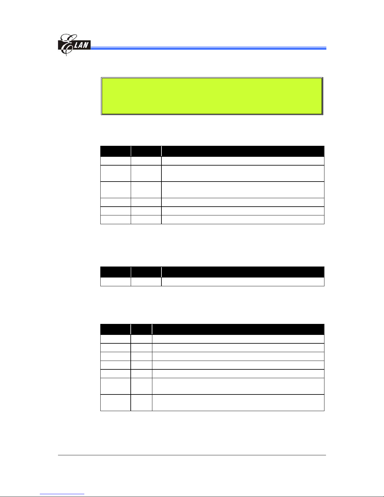
eSL/eSLS Series (+ eSLZ000) User’s Manual Architecture •••• 17
Chapter 2
Architecture
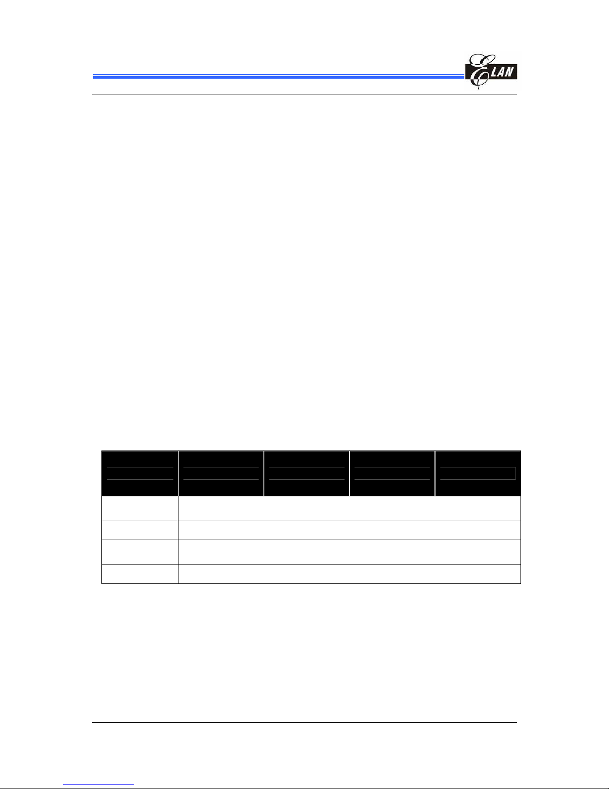
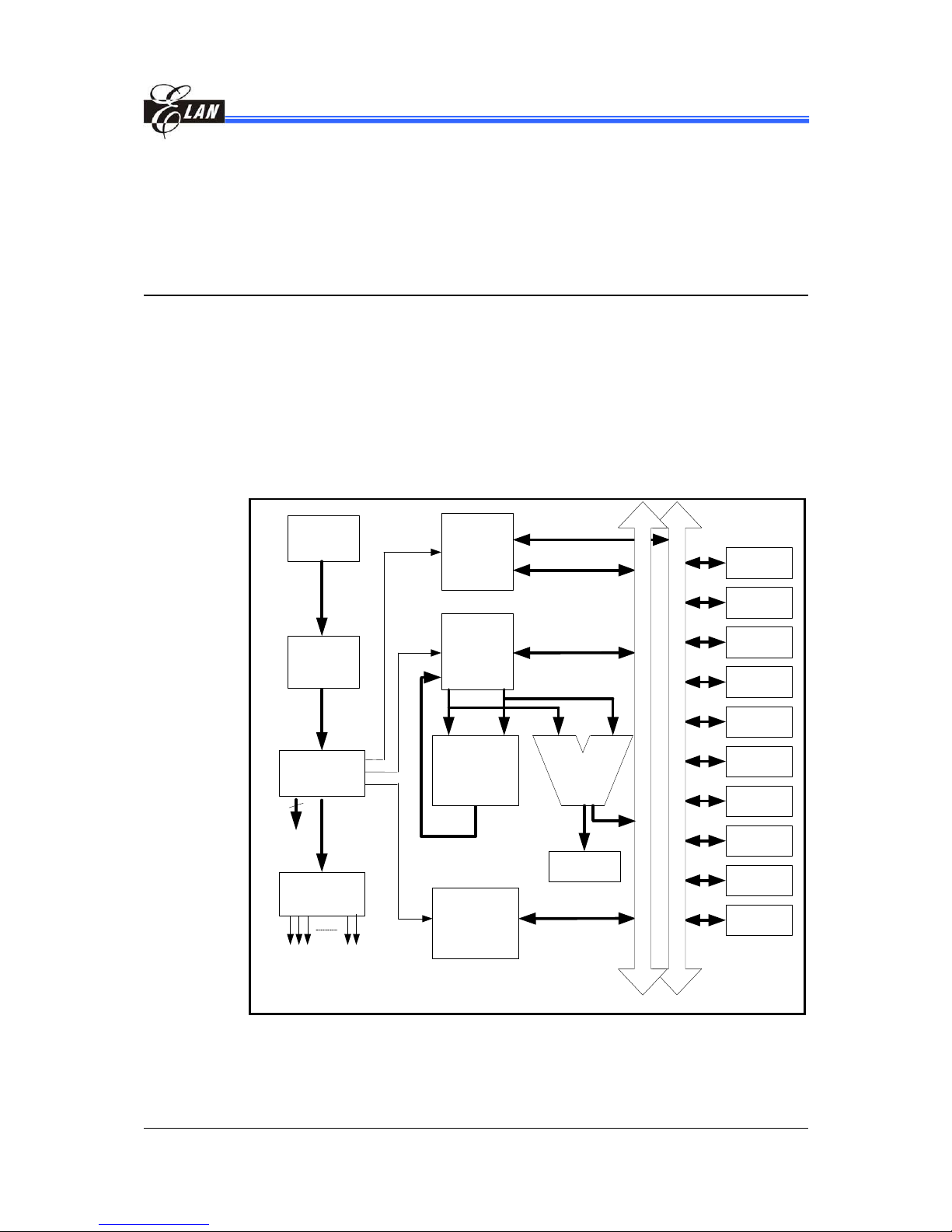
2.1 eSL System Block Diagram
As shown in the block diagram below, ELAN eSL Series (eSL/eSLS Series and
eSLZ000) utilize a modified Harvard architecture in such a way that the
memory is organized into two separated fields; Program ROM and Data RAM.
As the memory is separated, the central processing units can read/write data at
the same time. Furthermore, the I/O space has an independent address, i.e., the
I/O-mapped I/O. The different configurations of each domain are explained in
this chapter.
PWM
General
Purpose
Registers
Status Reg
17x17
Multiplier /
Divider
(+16 bit ALU)
Program
Counter
Instruction
Decoder
I/O Space
(SFR)
RAM Addressing
Reg Addressing
Port A~D
ADC
DAC
INT
Contol
Signals
ACC D
IMM
#16
Timer
RTC
WDT
SPI
OSC/PLL
ROM
Control
Unit
ALU
RAM
I/O Bus
Data Bus
I/O Direct Addressing
Figure 2-1 ELAN eSL Series System Block Diagram.
Chapter 2
18 •••• Architecture eSL/eSLS Series (+ eSLZ000) User’s Manual
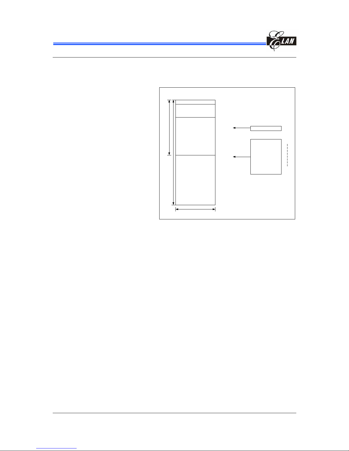
2.2 Program ROM and Data RAM Description
2.2.1 Program ROM/RAM
It includes 32K * 16-bit
on-chip ROM (for both
eSL & eSLS Series) or
RAM (eSLZ000 only)
for your program and
general data storage
utilization. Program
counter (PC) is the
dedicated counter for
program address, and is
automatically modified
by control flow
processing. The eight
general purpose
registers can be used as
Program ROM or RAM
pointers.
Program ROM/RAM
0x0000
0x7FFF (32767)
Reset Vector
0x0002
Interrupt Vector
Short Call
0x3FFF
Long Call
16-bit
Total
32K * 16-bit
Linear memory
space
PC
R0
R7
General
Purpose
Registers
(Indirect pointer)
Figure 2-2 eSL Series Program ROM Block Diagram
 Loading...