

Page 1

EPH3600
RISC II Series
Microcontroller
Product
Specification
DOC. VERSION 0.1
ELAN
MICROELECTRONICS CORP.
October 2007
Page 2
Trademark Acknowledgments:
IBM is a registered trademark and PS/2 is a trademark of IBM.
Windows is a trademark of Microsoft Corporation.
ELAN and ELAN logo are trademarks of ELAN Microelectronics Corporation.
Copyright © 2007 by ELAN Microelectronics Corporation
All Rights Reserved
Printed in Taiwan
The contents of this specification are subject to change wi t h out f urt her notice. ELAN Microelectronics assumes
no responsibility concerning the accuracy, adequacy, or completeness of this specification. ELAN
Microelectronics makes no commitment to update, or to keep current the information and material contained in
this specification. Such information and material may change to conform to each confirmed order.
In no event shall ELAN Microelectronics be made responsible for any claims attributed to errors, omissions, or
other inaccuracies in the information or material contained in this specification. ELAN Microelectronics shall
not be liable for direct, indirect, special incidental, or consequential damages arising from the use of such
information or material.
The software (if any) described in this specification is furnished under a license or nondisclosure agreement, and
may be used or copied only in accordance with the terms of such agreement.
ELAN Microelectronics products are not intended for use in life support appliances, devices, or systems. Use of
ELAN Microelectronics product in such applications is not supported and is prohib ited.
NO PART OF THIS SPECIFICATION MAY BE REPRODUCED OR TRANSMITTED IN ANY FORM OR
BY ANY MEANS WITHOUT THE EXPRESSED WRITTEN PERMISSION OF ELAN MICROELECTRONICS.
ELAN MICROELECTRONICS CORPORATION
Headquarters:
No. 12, Innovation Road 1
Hsinchu Science Park
Hsinchu, TAIWAN 308
Tel: +886 3 563-9977
Fax: +886 3 563-9966
http://www.emc.com.tw
Hong Kong:
Elan (HK) Microelectronics
Corporation, Ltd.
Flat A, 19F., World Tech Centre
95 How Ming Street, Kwun Tong
Kowloon, HONG KONG
Tel: +852 2723-3376
Fax: +852 2723-7780
elanhk@emc.com.hk
Shenzhen:
Elan Microelectronics
Shenzhen, Ltd.
3F, SSMEC Bldg., Gaoxin S. Ave. I
Shenzhen Hi-tech Industrial Park
(South Area), Shenzhen
CHINA 518057
Tel: +86 755 2601-0565
Fax: +86 755 2601-0500
USA:
Elan Information
Technology Group (U.S.A.)
PO Box 601
Cupertino, CA 95015
U.S.A.
Tel: +1 408 366-8225
Fax: +1 408 366-8225
Shanghai:
Elan Microelectronics
Shanghai, Ltd.
#23, Zone 115, Lane 572, Bibo Rd.
Zhangjiang Hi-Tech Park
Shanghai, CHINA 201203
Tel: +86 21 5080-3866
Fax: +86 21 5080-4600
Page 3

Contents
Contents
1 General Description.................................................................................................. 1
1.1 Applications........................................................................................................2
2 Features ..................................................................................................................... 2
2.1 MCU Features....................................................................................................2
2.2 Peripheral...........................................................................................................2
2.3 Internal Specification..........................................................................................3
2.4 Elan Software Support (Option) ......................................................................... 3
3 Block Diagram........................................................................................................... 4
4 Pin Assignment......................................................................................................... 5
5 Pin Description.......................................................................................................... 6
5.1 MCU System Pins (9 Pins)................................................................................. 6
5.2 I/O Ports (32 Pins).............................................................................................. 7
6 Code Options............................................................................................................. 8
7 Function Description ................................................................................................ 9
7.1 Reset Function................................................................................................... 9
7.1.1 Power-up and Reset Timing................................................................................9
7.1.2 Register Initial Values........................................................................................11
7.2 Oscillator System .............................................................................................13
7.2.1 32.768kHz Crystal or 32.8kHz RC....................................................................13
7.2.2 Phase Locked Loop (PLL).................................................................................13
7.3 MCU Operation Mode ...................................................................................... 15
7.4 Wake-up Function............................................................................................ 17
7.5 Interrupt............................................................................................................18
7.5.1 Input Port A Interrupt .........................................................................................18
7.5.2 Capture Input Interrupt......................................................................................19
7.5.3 Speech Timer Interrupt......................................................................................19
7.5.4 Timer 0, Timer 1, and Timer 2 Interrupts...........................................................19
7.5.5 Peripheral Interrupt............................................................................................20
7.6 Program ROM Map .......................................................................................... 20
7.7 Data ROM Map ................................................................................................ 21
7.8 RAM Map Register
(RAM Size: 128 Bytes + 32 Banks × 128 Bytes = 4224 Bytes)........................
7.8.1 Special and Control Register of RAM................................................................21
7.8.2 Other Un-banked Register of RAM:..................................................................25
7.8.3 Banked Register of RAM:(selected by BSR) ....................................................25
7.9 Special Register Description............................................................................ 25
7.9.1 Indirect Addressing Pointer 0............................................................................26
7.9.2 Indirect Addressing Pointer 1............................................................................27
21
Product Specification (V0.1) 10.11.2007 • iii
(This specification is subject to change without further notice)
Page 4

Contents
8 Peripheral................................................................................................................. 32
8.1 Timer 0 (16-bit Timer with Capture and Event Counter Functions).................. 32
8.1.1 Timer 0 Mode: ...................................................................................................32
8.1.2 Capture Mode: CPIN (Port B.5) Pin ..................................................................33
8.1.3 Event Counter Mode: EVIN (Port B.5) Pin ........................................................33
8.2 Timer 1 (8 Bits)................................................................................................. 37
8.3 Timer 2 (8 Bits)................................................................................................. 40
8.4 IR Generator: IROT (Port B.2) Pin.................................................................... 43
8.5 EL Timer (6 Bits)............................................................................................... 44
8.5.1 EL Generator Timing.........................................................................................46
8.6 Watchdog Timer (WDT).................................................................................... 47
8.7 Universal Asynchronous Receiver Transmitter (UART).................................... 48
8.7.1 Data Format in UART........................................................................................49
8.7.2 UART Modes.....................................................................................................49
8.7.3 UART Transmit Data.........................................................................................50
8.7.4 UART Receive Data..........................................................................................50
8.7.5 UART Baud Rate Generator.............................................................................51
8.7.6 UART Applicable Registers...............................................................................51
8.7.7 Transmit Counter Timing...................................................................................54
8.7.8 UART Transmit Operation (8-Bit Data with Parity Bit).......................................54
8.7.9 Receive Counter T iming....................................................................................55
8.8 A/D Converter................................................................................................... 57
8.8.1 A/D Converter Applicable Registers..................................................................58
8.8.2 Timing Diagram of General A/D Converter Application.....................................61
8.8.3 Correlation between A/D Converter and MCU Mode........................................61
8.8.4 A/D Converter Flowchart...................................................................................63
8.9 Serial Peripheral Interface (SPI)....................................................................... 65
8.9.1 Master Mode .....................................................................................................66
8.9.2 Slave Mode .......................................................................................................67
8.9.3 SPI Pin Descriptions..........................................................................................67
8.9.4 SPI Applicable Registers...................................................................................67
8.9.5 SPI Timing Diagrams.........................................................................................70
8.10 Speech Synthesizer.......................................................................................... 72
8.10.1 Speech Function................................................................................................72
8.11 DAC Function................................................................................................... 74
8.11.1 DAC Function Block Diagram ...........................................................................74
8.11.2 DAC Function Registers....................................................................................75
iv • Product Specification (V0.1) 10.11.2007
(This specification is subject to change without further notice)
Page 5

Contents
9 Electrical Characteristic ......................................................................................... 76
9.1 Absolute Maximum Ratings.............................................................................. 76
9.2 Recommended Operating Conditions.............................................................. 76
9.3 DC Electrical Characteristics............................................................................ 76
9.4 AC Electrical Characteristics............................................................................78
10 Application Circuit ................................................................................................. 79
11 Instruction Set......................................................................................................... 80
12 Pad Diagram ............................................................................................................83
Specification Revision History
Doc. Version Revision Description Date
0.1 Initial Preliminary Version 2007/10/12
Product Specification (V0.1) 10.11.2007 • v
(This specification is subject to change without further notice)
Page 6

Contents
vi • Product Specification (V0.1) 10.11.2007
(This specification is subject to change without further notice)
Page 7

1 General Description
The EPH3600 is an 8-bit RISC MCU embedded with following:
10 bits SAR A/D converter with touch screen controller
One 16-bit general timer with capture and event counter functions,
Two 8-bit timers IR generator
EL timer Watchdog timer
SPI UART
One current D/A.
Moreover, the EPH3600 is equipped with a large size user RAM and program/data
memory. The MCU is most suitable for products involving handwriting recognition
application that requires high performance with low cost solution; such as SMS,
Stylus Remote Controller, mobile phones, handwriting input device, etc.
The MCU’s core is ELAN’s second generation RISC (RISC II) based IC. The core is
specifically designed to provide a low power consumption portable device. It
supports FAST, SLOW, and Idle mode, as well as Sleep mode for low power
consumption application.
EPH3600
RISC II Series Microcontroller
IMPORTANT NOTES
■ Do not use Register BSR (05h) Bit 7 ~ Bit 5
■ Do not use Register BSR1 (07h) Bit 7 ~ Bit 5
■ Do not use Special Register (04h)
■ Do not use Special Register (1Bh)
■ Do not use Special Register (1Ch)
■ Do not use Special Register (1Fh)
■ Do not use Special Register (32h)
■ Do not use Special Register (33h)
■ Do not use Special Register (37h)
■ Do not use Special Register (38h)
■ Do not use Special Register (39h)
■ Do not use Special Register (45h)
■ Do not use Special Register (46h)
■ Do not use Special Register (47h)
■ Do not use Special Register (4Fh)
■ Do not use Special Register (50h)
■ Do not use Special Register (51h)
■ Do not use Special Register (52h)
■ Do not use Special Register (53h)
■ Do not use JDNZ and JINZ at FSR1 (09h) special register
■ Do not use Register TABPTRH (0Dh) Bit 6
Product Specification (V0.1) 10.11.2007 • 1
(This specification is subject to change without further notice)
Page 8

EPH3600
RISC II Series Microcontroller
1.1 Applications
Handwriting Recognition
Dictionary, Data Bank
Stylus Remote Controlller
2 Features
2.1 MCU Features
8-bit RISC MCU
8×8 multiplier with controllable signed or unsigned operation
Operating voltage and speed: 16MHz~11MHz @ 2.9V~3.6V, 10MHz @
2.2V~3.6V, 4MHz @ 1.6V~3.6V
One Instruction cycle time = 2 × System clock time
Program ROM addressing: 16K words maximum
Data ROM addressing: 256K words maximum
128 bytes un-banked RAM including special registers and common registers
32×128 bytes banked RAM
RAM stack has a maximum of 128 levels
Table Look Up function is fast and highly efficient when implemented with Repeat
instruction
Register-to-Register move instruction
Compare and Branch in one instruction (2 cycles)
Single Repeat function (256 repeat times maximum)
Decimal Add & Sub instruction
Full range Call and Jump capability (2 cycles)
2.2 Peripheral
One input port (Port A) and 24 gene ral I/O pins (Port B, Port C, Port D)
1-channel Speech Synthesizer
16-bit timer (Timer 0) with capture and ev ent counter functions
8-bit timer (Timer 1) with wake-up function
8-bit timer (Timer 2)
8-bit IR generator
2 • Product Specification (V0.1) 10.11.2007
(This specification is subject to change without further notice)
Page 9

6-bit EL Timer output
A current D/A for speech application
8-bit Watchdog Timer
10 bits resolution SAR A/D converter with 6 channels general analog input and 2
channels for touch panel application
SPI (Serial Peripheral Interface)
UART (Universal Asynchronous Receiver and Transmitter)
2.3 Internal Specification
Watchdog Timer with on-chip RC oscillator
MCU mode: Sleep Mode, Idle Mode, Slow Mode, and Fast Mode
Supports either RC oscillation or crystal oscillation system clock
EPH3600
RISC II Series Microcontroller
PLL can be turned on at Fast Mode, and controlled by PEN bit when MCU is in
Slow Mode or Idle Mode
MCU Wake-up function includes input wake up, Ti mer 1 wake up, touch panel
wake up, SPI wake up, and A/D wake up
MCU interrupt function includes Input Port interrupt, Touch Panel interrupt,
Capture interrupt, Speech Timer interrupt, Timer Interrupt (Timers 0~2), A/D
interrupt, SPI interrupt, and UART interrupt
MCU reset function includes power-on reset, RSTB pin reset, and Watchdog
timer reset
2.4 Elan Software Support (Option)
Hand writing recognition core
1-channel Speech
ADPCM decoder
ADPCM encoder
Product Specification (V0.1) 10.11.2007 • 3
(This specification is subject to change without further notice)
Page 10
EPH3600
RISC II Series Microcontroller
3 Block Diagram
VREX
RSTB TEST VDD OSCI OSCO
8 x 8 Mul
PRODH PRODL
PRODL
Addressing Co n tro l U n it
Speech Synthesizer
D/A
SAR A/D
I/O Control
ALU
Shifter
UART
Timer 0 ~ Timer 2 /
EL / WDT Timer
Key IO
AVDD
IR Generator
SPI
Timing Generator
PLLC
RAM
ROM
88
8
Po rtD PortC PortB P ortA
Figure 1-1 EPH3600 Block Diagram
4 • Product Specification (V0.1) 10.11.2007
8
VSS
(This specification is subject to change without further notice)
Page 11
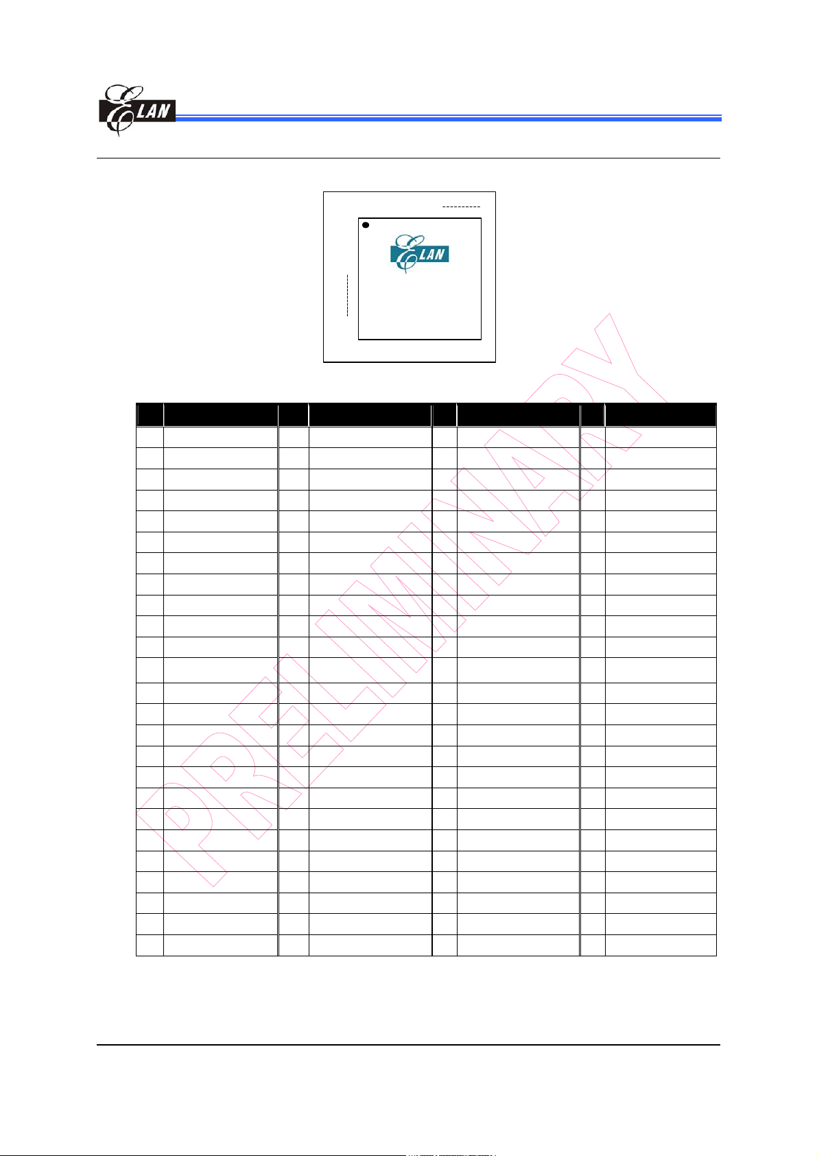
4 Pin Assignment
No. Pin Name No. Pin Name No. Pin Name No. Pin Name
1 N.C. 26 Port C.6 (YN) 51 N.C. 76 N.C.
2 N.C. 27 Port C.5 (ADIN3/XP) 52 N.C. 77 N.C.
3 N.C. 28 Port C.4 (ADIN4/YP) 53 PD.6 (SPISDO) 78 N.C.
4 N.C. 29 N.C. 54 PD.7 (SPISDI) 79 N.C.
5 N.C. 30 N.C. 55 Port A.0 80 N.C.
6 N.C. 31 Port C.3 (ADIN5) 56 Port A.1 81 N.C.
7 N.C. 32 Port C.2 (ADIN6) 57 Port A.2 82 N.C.
8 N.C. 33 Port C.1 (ADIN7) 58 Port A.3 83 N.C.
9 N.C. 34 Port C.0 (ADIN8) 59 Port A.4 84 N.C.
10 N.C. 35 Port B.0 60 Port A.5 85 N.C.
11 N.C. 36 Port B . 1 ( DAO) 61 Port A.6 86 N.C.
12 N.C. 37 Port B.2 (IROT) 62 Port A.7 87 N.C.
13 N.C. 38 Port B.3 (EL CK) 63 N.C. 88 N.C.
14 N.C. 39 Port B.4 (CHOP) 64 N.C. 89 N.C.
15 N.C. 40 Port B.5 (EVIN/CPIN) 65 N.C. 90 N.C.
16 N.C. 41 Port B.6 (UTXD) 66 N.C. 91 N.C.
17 N.C. 42 Port B.7 (URXD) 67 N.C. 92 N.C.
18 TEST 43 VDD 68 N.C. 93 N.C.
19 PLLC 44 VSS 69 N.C. 94 N.C.
20 OSCI 45 Port D.0 70 N.C. 95 N.C.
21 OSCO 46 Port D.1 71 N.C. 96 N.C.
22 RSTB 47 Port D.2 72 N.C. 97 N.C.
23 VREX 48 Port D.3 73 N.C. 98 N.C.
24 AVDD 49 PD.4 (SPISS) 74 N.C. 99 N.C.
25 Port C.7 (XN) 50 PD.5 (SPISCK) 75 N.C. 100 N.C.
EPH3600
RISC II Series Microcontroller
100 99 98 ......
1
2
3
EPH3600
(top view)
Product Specification (V0.1) 10.11.2007 • 5
(This specification is subject to change without further notice)
Page 12
EPH3600
RISC II Series Microcontroller
5 Pin Description
5.1 MCU System Pins (9 Pins)
Name
AVDD
VSS
VDD
VSS
RSTB I
TEST I Normally connected to VSS. Reserved for testing use.
OSCI/RC
OSCO
PLLC I
VREX I/O
I/O/P
Type
P
P
I
O
Description
Analog positive power supply. The range is 2.2V~3.6V. Connect to VSS
through capacitors (0.1µF).
Digital and Analog positive power supply. Range is 2.2V~3.6V. Connect
to VSS through capacitor (0.1µF).
System reset input with built-in pull-up resistor (100KΩ Typical).
Low: RESET asserted
High: RESET released
RC or Crystal selection by Code Option.
32768 Hz oscillator pins. Connect to VSS through capacitor (20pF)
RC oscillator connector pin. Connect to VDD through a resistor (2MΩ).
PLL capacitor connector pin. Connect to VSS through capacitor
(0.047µF).
External or internal reference voltage for A/D converter. Connect to VSS
through capacitor (0.1µF).
6 • Product Specification (V0.1) 10.11.2007
(This specification is subject to change without further notice)
Page 13

5.2 I/O Ports (32 Pins)
EPH3600
RISC II Series Microcontroller
Name
Port A I
Port B
Port C
Port D
I/O/P
Type
I/O
I
O
I
O
O
O
O
O
I/O
O
O
I
I
I
I
I
I
I/O
I
O
I/O
I
I/O
Description
General Input port for special functions, i.e., Wake-up and
Interrupt
Bit 7: ON key input
Bits 6~0: Key matrix input pins
General Input/Output port
Bit 7: UART Rx pin
Bit 6: UART Tx pin
Bit 5: Event Counter/Capture input pin
Bit 4: EL CHOP output pin
Bit 3: EL CK output pin
Bit 2: IR output pin
Bit 1: Current D/A output pin
Bit 0: I/O pin
General Input/Output port
Bit 7: Touch screen X direction negative pin
Bit 6: Touch screen Y direction negative pin
Bit 5: Touch screen X direction positive pin & A/D input Channel 3
Bit 4: Touch screen Y direction positive pin & A/D input Channel 4
Bit 3: A/D input Channel 5
Bit 2: A/D input Channel 6
Bit 1: A/D input Channel 7
Bit 0: A/D input Channel 8
General Input/Output port
Bit 7: Serial data input pin
Bit 6: Serial data output pin
Bit 5: Serial clock Input/Output pin
Bit 4: /Slave Select pin
Bit 3~0: I/O pin
Product Specification (V0.1) 10.11.2007 • 7
(This specification is subject to change without further notice)
Page 14
EPH3600
RISC II Series Microcontroller
6 Code Options
The Code Options are located at Address 0x000C~0x0013 of the Program ROM:
Oscillator (OSCSEL) : “RC” oscillator
“Crystal” oscillator (Default)
Initial mode after reset : “Slow” mode
“Fast” mode (Default)
Port C.7 function selection bit : “XN for touch panel”
“General I/O function” (Default)
Port C.6 function selection bit : “YN for touch panel”
“General I/O function” (Default)
Port C.5 function selection bit : “XP for touch panel/ADIN3”
“General I/O function” (Default)
Port C.4 function selection bit : “YP for touch panel/ADIN4”
“General I/O function” (Default)
Port C.3 function selection bit : “ADIN5”
“General I/O function” (Default)
Port C.2 function selection bit : “ADIN6”
“General I/O function” (Default)
Port C.1 function selection bit : “ADIN7”
“General I/O function” (Default)
Port C.0 function selection bit : “ADIN8”
“General I/O function” (Default)
DAC function selection bits:
DAC Function Selection Port B.0 and Port B.1 Function
DAC is used Port B.1 is DAO for D/A, Port B.0 is General I/O
DAC usage is prohibited General I/O (Default)
Select UART standard baud rate : “PLL frequency is 9.83MHz” (Default)
“PLL frequency is 14.745MHz”
Port A pull-h and DAC control bit: “PAPUR register, DAC bit ineffective” (Default)
“PAPUR register, DAC bit effective”
EL Output TIming : “Output is from carrier gating with 128Hz and CKP” (Default)
“CHOP output is directly from carrier”
8 • Product Specification (V0.1) 10.11.2007
(This specification is subject to change without further notice)
Page 15
7 Function Description
7.1 Reset Function
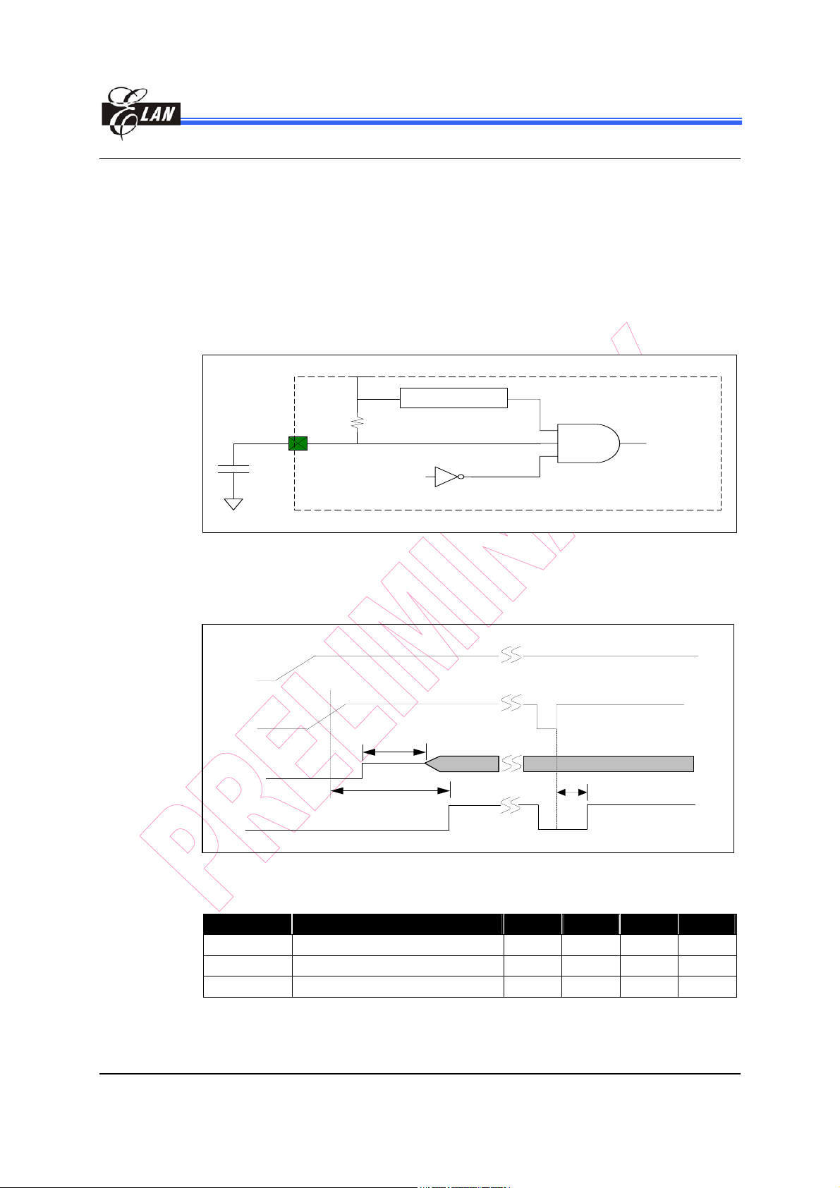
A Reset can be caused by:
Power-on voltage detector reset and power-on reset
WDT timeout
RSTB pin pull low
VDD
EPH3600
RISC II Series Microcontroller
P o w e r-o n R e se t
RSTB
+
0.1uF
WDT Reset
Figure 7-1 On-chip Reset Circuit
7.1.1 Power-up and Reset Timing
VDD
RSTB
Tpwr
OSC
Twup
CPU Work
/Chip R eset
Twup1
Figure 7-2 Power-up and Reset Timing
Symbol Characteristics Min. Typical Max. Unit
Tpwr Oscillator start up time 100 226 300 ms
Twup CPU warm up time 260 340 550 ms
Twup1 CPU reset time 18 22 44 ms
Product Specification (V0.1) 10.11.2007 • 9
(This specification is subject to change without further notice)
Page 16

EPH3600
RISC II Series Microcontroller
Status (R0Fh)
Bit 7 Bit 6 Bit 5 Bit 4 Bit 3 Bit 2 Bit 1 Bit 0
/TO /PD SGE SLE OV Z DC C
Bit 0 (C): Carry flag or inverse of Borrow flag (B)
When in SUB operation, borrow flag is indicated by the inverse of carry
bit (B = /C)
Bit 1 (DC): Auxiliary carry flag
Bit 2 (Z): Zero flag
Bit 3 (OV): Overflow flag. Use in signed operation when Bit 6 carry into or borrow
from a signed bit (Bit 7).
Bit 4 (SLE): Computation result is less than or equal to zero (Negative value) after
a signed arithmetic. It is only affected by a HEX arithmetic instruction.
Bit 5 (SGE): Computation result is greater than or equal to zero (Positive value) after
a signed arithmetic. It is only affected by a HEX arithmetic instruction.
NOTE
1. When OV=1 after a signed arithmetic, user can check the SGE and SLE bits to
determine whether an overflow (carry into a signed bit) or underflow (borrow from
a signed bit) occurs.
OV=1 and SGE=1 → overflow occurs
OV=1 and SLE=1 → underflow occurs
2. When overflow occurs, you should clear the MSB of the Accumulator in order to
get the correct value.
When underflow occurs, you should set the MSB of the Accumulator in order to
get the correct value.
Example 1: ADD a positive value to another positive value, and ACC signed bit will
be affected.
MOV ACC, #60h ; Signed number +60h
ADD ACC, #70h ; +60h ADD WITH +70h
After instruction: ACC = 0D0h
SGE=1, means the result is greater than or equal to 0 (positive value)
OV=1, means the result is carry into a signed bit (Bit 7), overflow occurs.
Correct the signed bit: ACC = 50h (Clear the signed bit)
The actual result = +80h (OV=1) + 50h = +0D0h
Example 2: SUB a positive value from a negative value, and ACC signed bit will be
affected.
MOV ACC, #50h ; Signed number +50h
SUB ACC, #90h ; +50h SUB from –70h (Signed
number of 90h)
10 • Product Specification (V0.1) 10.11.2007
(This specification is subject to change without further notice)
Page 17
EPH3600
RISC II Series Microcontroller
After instruction: ACC = 40h
SLE=1, means the result is less than or equal to 0 (negative value)
OV=1, means the result is borrow from a signed bit (Bit 7), underflow
occurs.
Correct the signed bit: ACC = 0C0h (Set the signed bit)
The actual result = –80h (OV=1) + 0C0h (signed number of 0C0h) = 40h
Bit 6 (/PD): Reset to 0 when entering SLEEP mode. Set to 1 by “WDTC” instruction,
power-on reset, or during a Reset pin low condition.
Bit 7 (/TO): Reset to 0 during WDT time out reset. Set to 1 by “WDTC” instruction,
entering SLEEP MODE, power-on reset, or during a Reset pin low
condition.
When a reset occurs, the special function register will be reset to its initial value
except for the /TO and /PD bits of the STATUS register.
Bit 7 (/TO) Bit 6 (/PD) Event
0 0 WDT time out reset from SLEEP mode
0 1 WDT time out reset (not SLEE P mode)
1 0 Reserved
1 1 Power on or RSTB pin low condition
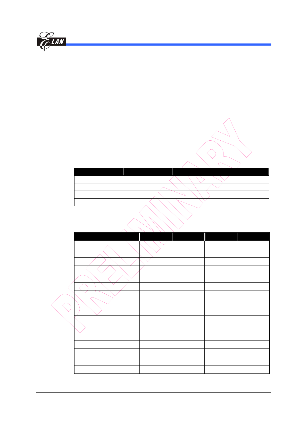
7.1.2 Register Initial Values
Special Register:
Addr. Name Initial Value Addr. Name Initial Value
00h INDF0 −−−− −−−−
01h FSR0 0000 0000 11h PRODL uuuu uuuu
02h PCL 0000 0000 12h PRODH uuuu uuuu
03h PCM 0000 0000 13h ADOTL 0−0− −0uu
04h (Not Used) −−−− −−−− 14h ADOTH uuuu uuuu
05h BSR −−−0 0000 15h UARTTX ×××× ××××
06h STKPTR 0000 0000 16h UARTRX ×××× ××××
07h BSR1 −−−0 0000 17h Port A ×××× ××××
08h INDF1 −−−− −−−−
09h FSR1 1000 0000 19h Port C ×××× ××xx
0Ah ACC ×××× ×××× 1Ah Port D ×××× xxxx
0Bh TABPTRL 0000 0000 1Bh (Not Used) −−−− −−−−
0Ch TABPTRM 0000 0000 1Ch (Not Used) −−−− −−−−
0Dh TABPTRH 0−00 0000 1Dh R1D ×××x x×××
0Eh CPUCON 0−−0 000c
0Fh STATUS cu×× ××××
1
10h TRL2 uuuu uuuu
1
18h Port B ×××x x×××
2
1Eh R1E ×××x x×××4
3
1Fh (Not Used) −−−− −−−−
4
Product Specification (V0.1) 10.11.2007 • 11
(This specification is subject to change without further notice)
Page 18
EPH3600
RISC II Series Microcontroller
Control Register:
Addr. Name Initial Value Addr. Name Initial Value
20h PFS 0010 0000 3Bh PCCON 0000 0000
21h STBCON 0−−− −−−− 3Ch PLLF ×××× ××××
22h INTCON 0000 0000 3Dh T0CL 0000 0000
23h INTSTA 0000 0000 3Eh T0CH 0000 0000
24h TRL0L uuuu uuuu 3Fh SPICON 0000 0000
25h TRL0H uuuu uuuu 40h SPISTA −−00 0000
26h TRL1 uuuu uuuu 41h SPRL ×××× ××××
27h TR01CON 0000 0000 42h SPRM ×××× ××××
28h TR2CON 0000 0000 43h SPRH ×××× ××××
29h TRLIR uuuu uuuu 44h SFCR 0000 0000
2Ah ELCON 00uu uuuu 45h (Not Used) ×××× ××××
2Bh POST_ID −−11 −−00 46h (Not Used) ×××× ××××
2Ch ADCON 0101 0000 47h (Not Used) ×××× ××××
2Dh PAINTEN 0000 0000 48h SPHDR 0000 0000
2Eh PAINTSTA 0000 0000 49h SPHTCON 0000 0000
2Fh PAWAKE 0000 0000 4Ah SPHTRL 0000 0000
30h UARTCON 0000 0010 4Bh VOCON 0−−−000
31h UARTSTA 0000 0000 4Ch TR1C 1111 1111
32h (Not Used) −−−− −−−− 4Dh TR2C 1111 1111
33h (Not Used) −−−− −−−− 4Eh ADCF uuuu uuuu
34h DCRB 1111 1111 4Fh (Not Used) −−−− −−−−
35h DCRC 1111 1111 50h (Not Used) −−−− −−−−
36h DCRDE −−−− 0011 51h (Not Used) −−−− −−−−
37h (Not Used) −−−− −−−− 52h (Not Used) −−−− −−−−
38h (Not Used) −−−− −−−− 53h (Not Used) −−−− −−−−
39h (Not Used) −−−− −−−− 54h PAPUR 0000 0000
3Ah PBCON 0000 0000 55h PACON −−−− 0110
Legend: “×” = unknown “−” = unimplemented, read as “0”
“u” = unchanged “c” = value depending on the condition
1
Not a physical register.
2
Bit 0 (MS0) of RE (CPUCON) is reloaded from “INIM” bit of code option when the
MCU is reset.
3
If it is a power-on reset or RSTB pin is at low condition, the /TO bit and /PD bit of RF
(STATUS) are set to “1”. If it is a WDT time out reset, the /TO bit is cleared and /PD
bit is unchanged.
4
R1D, R1E are generated register RAM.
5
PAPUR can be used only by the code option setting.
5
12 • Product Specification (V0.1) 10.11.2007
(This specification is subject to change without further notice)
Page 19
××=
××=
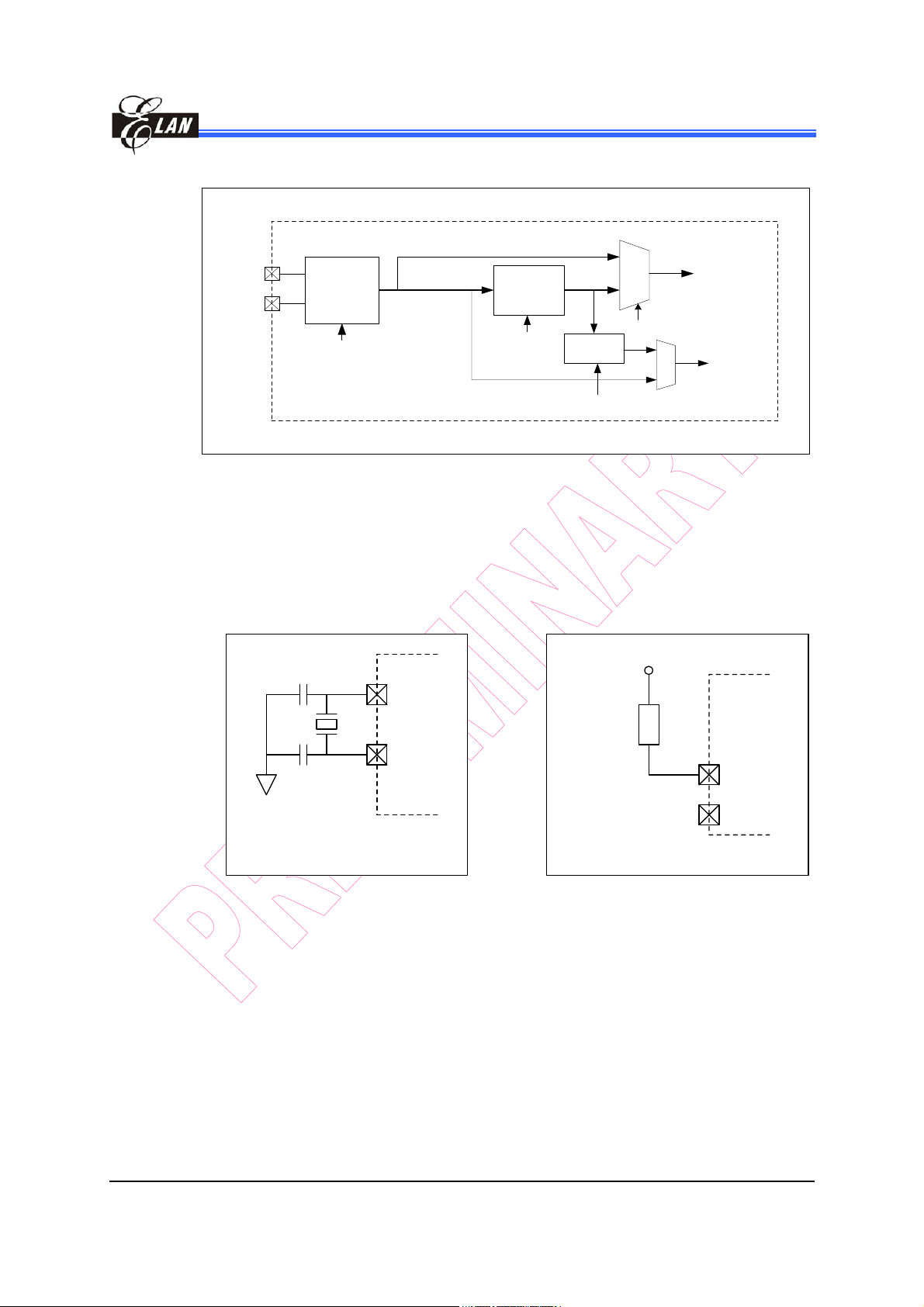
7.2 Oscillator System
EPH3600
RISC II Series Microcontroller
OSCI
OSCO
32.8kHz
RC/Crystal
Osc.
OSCSEL
of
Code Option
PLL
PEN
Fosc
A/D Clock
Factor
F
PLL
FSS
0
1
MS0
Fsystem
F
A/D
Figure 7-3 Oscillator System Function Block Diagram
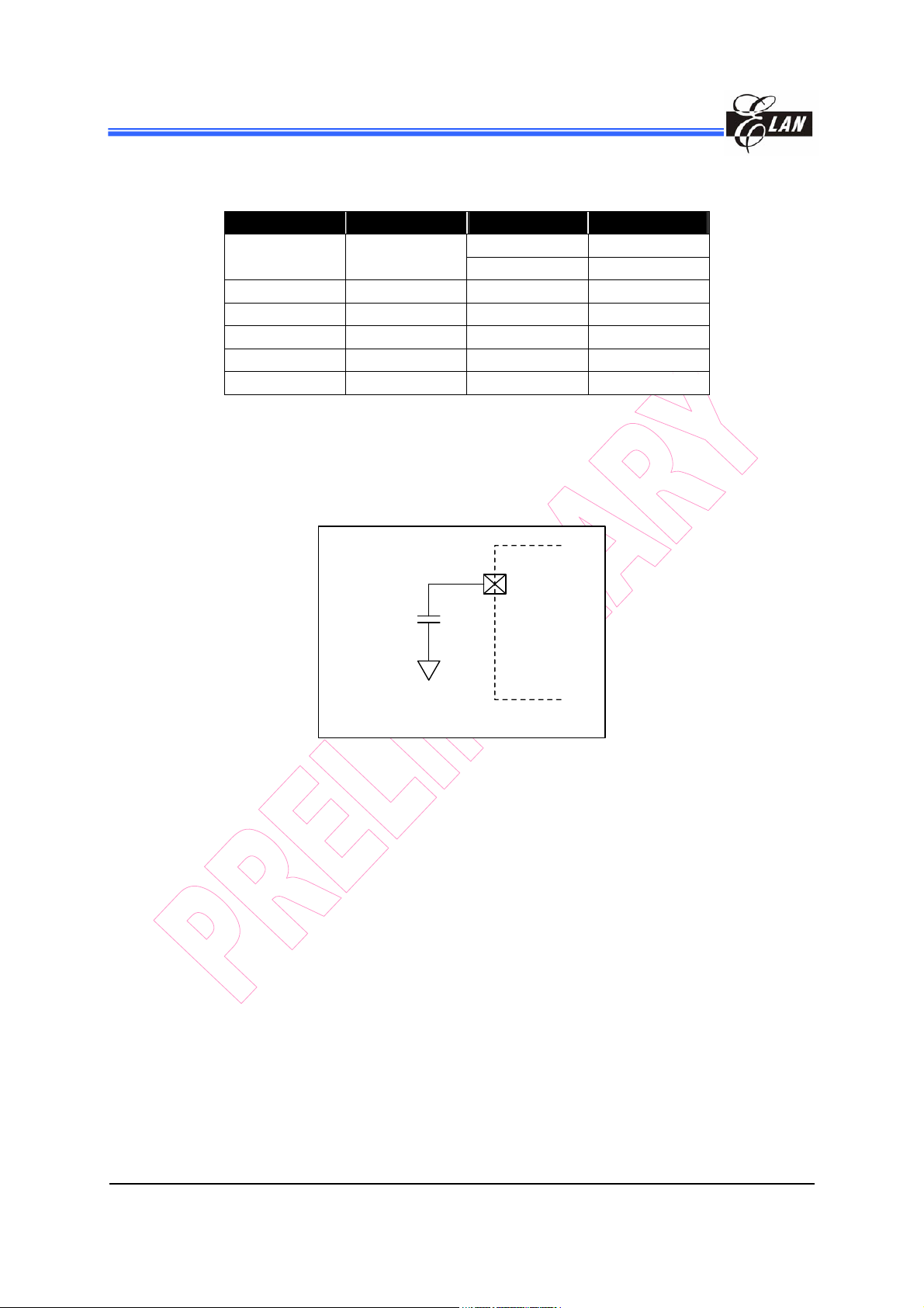
7.2.1 32.768kHz Crystal or 32.8kHz RC
For the 32.8kHz RC oscillator, connect a 2MΩ pull-up resistor to OSCI pin and the
OSCO pin should be floating.
For the 32.768kHz Crystal oscillator, connect the crystal between OSCI and OSCO
pins. Then connect the OSCI and OSCO pins to ground through a 20pF capacitor.
VDD
OSCI
2Mohm
OSCO
OSCI
OSCO
32.768kHz Crystal
Oscillator
32.8kHz RC Oscillator
Figure 7-4 Crystal and RC Oscillator Circuit Diagram
7.2.2 Phase Locked Loop (PLL)
PLLF (R3Ch): Store the actual PLL frequency value. It is used to check whether
the PLL frequency is stable or not.
2
PFS (R20h): Target PLL frequency select register. System clock can be fine
tuned from 0.983MHz to 16MHz. The initial value of the PFS
register after a chip reset is set at “20h” (F
2
arg
FPLLFF
OSCactual
=2.097 MHz)
PLL
FPFSF
OSCett
Product Specification (V0.1) 10.11.2007 • 13
(This specification is subject to change without further notice)
Page 20
EPH3600
RISC II Series Microcontroller
PFS Register Ftarget (MHz) PFS Register Ftarget (MHz)
0~14 N.A.1
15 0.983 122 7.995
31 2.032 137 8.978
46 3.015 150 9.83
61 3.998 153 10.027
76 4.981 255 16.712
1
PFS=0~14 is not available.
2
When UART is enabled, the system clock should be 9.83 MHz (PFS=150) or 14.745 MHz
(PFS=225).
The table is based on 32.768kHz oscillator frequency.
The Maximum range of PLL is 983 kHz ~ 16.712 MHz.
92 6.029
107 7.012
2
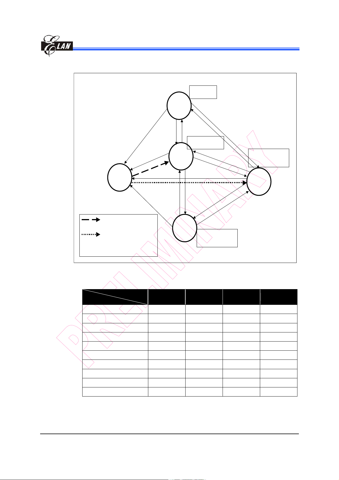
PLLC
0.047uF
PLL Osc illa t o r
Figure 7-5 PLL Oscillator Circuit Diagram
14 • Product Specification (V0.1) 10.11.2007
(This specification is subject to change without further notice)
Page 21
7.3 MCU Operation Mode
RESET
operation
FA S T MODE is th e in itial m o d e
after Reset
SLOW MODE is th e in itia l mode
after Reset
Select by IM bit of Code Option register
Reset
Reset
Reset Release
Wakeup
& MS0=1
Reset Release
Reset
SLEEP
MODE
(CPU stops)
MODE
Reset
wakeup
& MS0=1
MS1= 0 &
“SLEP”
32K OSC.:oscillating
PLL:turned on
FAST
MS1=1 &
“SLEP”
IDL E
MODE
(CPU stops)
32K OSC.:stop
PLL: stopped
Wakeup
& MS0=0
MS0=1
MS0=0
MS1=1 &
“SLEP”
32K O S C.:Oscillating
PEN=0->PLL stopped
PEN=1->PLL turned on
EPH3600
RISC II Series Microcontroller
MS1=0 &
“SLEP”
Wakeup
& MS0=0
32K OSC.:oscil la ti n g
PEN=0->PL L : stopped
PEN=1->PL L turned on
SLOW
MODE
Figure 7-6 Operation Block Diagram
MCU Mode with Function Table:
Mode
Device
OSC (32.768kHz) × √ √ √
Fsystem × × From OSC From PLL
PLL × √ √ √
A/D conversion × √ 2 √ √
Timers 0~2, IR generator × √ √ √
INT × 1 × 1 √ √
SPI √ (slave) √ (slave) √ √
UART × × × √
Speech Synthesizer × × × √
Current D/A × × √ √
Legend: “ √ ” = function is available if enabled “ × ” = function is Not available
1
Interrupt flag will be recorded but not executed until the MCU wakes up.
2
It is recommended to operate the A/D converter in Idle mode to lower the noise couple from
the MCU clock.
SLEEP IDLE SLOW FAST
Product Specification (V0.1) 10.11.2007 • 15
(This specification is subject to change without further notice)
Page 22
EPH3600
RISC II Series Microcontroller
CPUCON (R0Eh):
Bit 7 Bit 6 Bit 5 Bit 4 Bit 3 Bit 2 Bit 1 Bit 0
PEN - - SMCAND SMIER GLINT MS1 MS0
Sleep Mode: When MS1 bit is set to ‘0’ and “SLEP” instruction is ex ecuted, the
Idle Mode: When MS1 bit is set to ‘1’ and “SLEP” instruction is executed, the
Slow Mode: When MS0 bit is set to ‘0’, the MCU will enter into Slow mode.
Fast Mode: When MS0 bit is set to ‘1’, the MCU will enter into Fast mode.
PLL enable: It is only effective when the MCU is in Idle mode or SLOW mode.
MCU Mode PEN Bit PLL On/Off
SLEEP × Off
IDLE/SLOW
FAST × On
MCU will enter into Sleep mode.
MCU will enter into Idle mode.
0 Off
1 On
F
PLL
Target+5%
Target
T arget-5 %
Ts
FAS T M O D E
Ts
MS0
System
clock
Target
32.768K
0m s
SLOW
MODE
0m s
0.244ms
Figure 7-7 MCU Operation Timing Diagram
NOTE
1. Switch from Slow mode to Fast mode at Time = 0ms
2. The System clock will switch to FPLL after 8 oscillation clocks, and the system
clock will then increase to about hundreds of kHz.
3. The PLL frequency will be stable (±5%) at Time = Ts (2ms ~ 5ms).
Time
Tim e
16 • Product Specification (V0.1) 10.11.2007
(This specification is subject to change without further notice)
Page 23
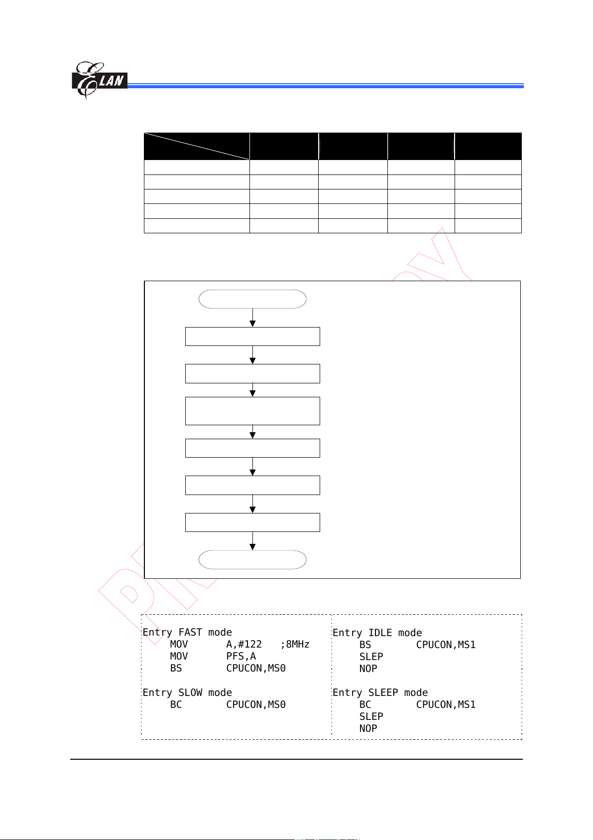
7.4 Wake-up Function
EPH3600
RISC II Series Microcontroller
Mode
Device
I/O wake up √ √ × ×
Touch panel wake up √ √ × ×
Timer1 wake up × √ × ×
A/D wake up × √ × ×
SPI wake up √ (Slave) √ (Slave) × ×
Legend: √ = Function is available if en abled × = Function is NOT available
Sleep Idle Slow Fast
Flowchart:
Change PLL F requency
BS CPUCO N, PEN Turn on the PLL
BC CPUCON, MS0 Change CPU to Slow mode
M O V A ,# 1 2 2
M O V P F S ,A
Chan ge PLL fre quency to
8MHz
SCALL DLY5m s
BS CPUCO N, M S0
BC CPUCON, PEN
G o to M a in R o u tin e
Code Example:
Entry FAST mode
MOV A,#122 ;8MHz
MOV PFS,A
BS CPUCON,MS0
Entry SLOW mode
BC CPUCON,MS0
D e la y fo r 5 m s to w a it fo r
PLL to be stable
Change CPU to Fast m ode
T u rn o ff th e P L L
Entry IDLE mode
BS CPUCON,MS1
SLEP
NOP
Entry SLEEP mode
BC CPUCON,MS1
SLEP
NOP
Product Specification (V0.1) 10.11.2007 • 17
(This specification is subject to change without further notice)
Page 24
EPH3600
RISC II Series Microcontroller
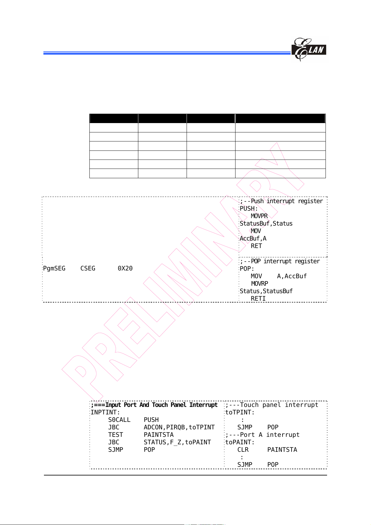
7.5 Interrupt
When an interrupt occurs, the GLINT bit of the CPUCON register is reset to 0, which
disables all interrupts, including Level 1 ~ Level 5. Setting this bit to 1 will enable all
un-mask interrupts.
Interrupt Level Interrupt Source Start Address Remarks
RESET 0x00000
Level 1 Input Port 0x00002 PAINT, PIRQB
Level 2 Capture 0x00004 CPIF
Level 3 Speech T imer 0x00006 SPHTI
Level 4 Timers 0~2 0x00008 TMR0I, TMR1I, TMR2I
Level 5 Peripheral 0x0000A UERRI, UTXI, URXI, ADIF, SRBFI
Code Example:
; ***** Reset program
ResetSEG CSEG 0X00
LJMP MSTART ;(0X00) Initialize
LJMP INPTINT ;(0X02) Input Port and Touch Panel INT
LJMP CAPINT ;(0X04) Capture Input INT
LJMP SPHINT ;(0X06) Speech Timer INT
LJMP TIMERINT ;(0X08) Timer-0,1,2 INT
LJMP PERIPH ;(0X0A) Peripheral INT
PgmSEG CSEG 0X20
;--Push interrupt register
PUSH:
MOVPR
StatusBuf,Status
MOV
AccBuf,A
RET
;--POP interrupt register
POP:
MOV A,AccBuf
MOVRP
Status,StatusBuf
RETI
7.5.1 Input Port A Interrupt
1. Port A Interrupt (Falling edge trigger): Port A is used as external interrupt/wake-up
input.
2. Touch Panel Interrupt (Level trigger): When Port C.7 ~ Port C.4 (X+, X-, Y+ and Y-)
are connected to touch panel input pins and
touch panel is touched, PIRQB interrupt
occurs.
Code Example:
;===Input Port And Touch Panel Interrupt
INPTINT:
S0CALL PUSH
JBC ADCON,PIRQB,toTPINT
TEST PAINTSTA
JBC STATUS,F_Z,toPAINT
SJMP POP
18 • Product Specification (V0.1) 10.11.2007
(This specification is subject to change without further notice)
;---Touch panel interrupt
toTPINT:
:
SJMP POP
;---Port A interrupt
toPAINT:
CLR PAINTSTA
:
SJMP POP
Page 25
EPH3600
RISC II Series Microcontroller
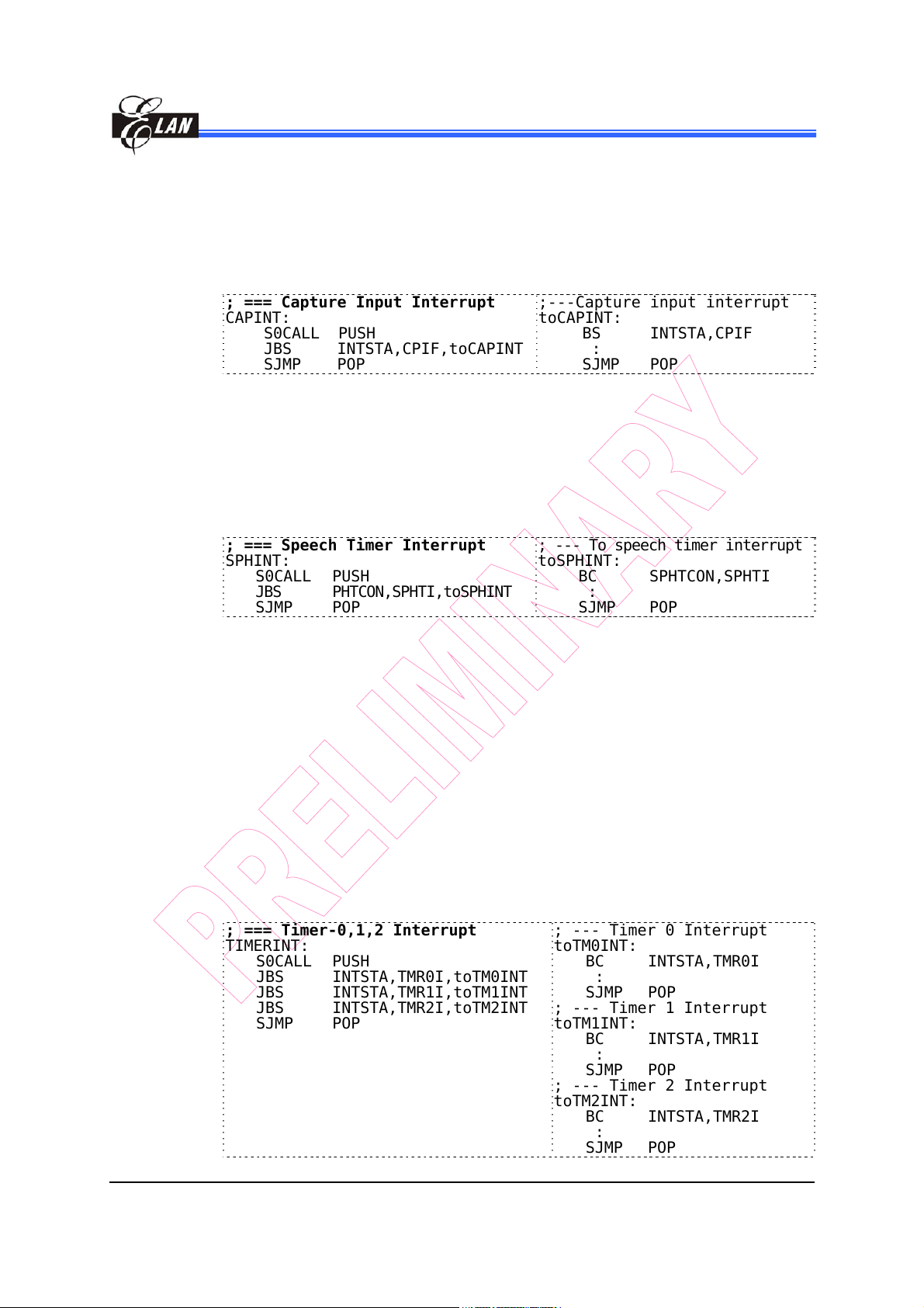
7.5.2 Capture Input Interrupt
The Capture function is used to capture an input event at rising to falling edge, falling
to rising edge, rising to rising edge, or falling to falling edge. When every event input
edge is detected, a Capture interrupt occurs.
Code Example:
; === Capture Input Interrupt
CAPINT:
S0CALL PUSH
JBS INTSTA,CPIF,toCAPINT
SJMP POP
;---Capture input interrupt
toCAPINT:
BS INTSTA,CPIF
:
SJMP POP
7.5.3 Speech Timer Interrupt
Speech Timer is an 11-bit timer for time counting. When the counting value of the
Speech Timer underflows, an interrupt occurs and the SPHTRL value will be reloaded
to counting value.
Code Example:
; === Speech Timer Interrupt
SPHINT:
S0CALL PUSH
JBS PHTCON,SPHTI,toSPHINT
SJMP POP
; --- To speech timer interrupt
toSPHINT:
BC SPHTCON,SPHTI
:
SJMP POP
7.5.4 Timer 0, Timer 1, and Timer 2 Interrupts
1. Timer 0 Interrupt: Timer 0 is a 16-bit timer for general time counting. When the
counting value is larger than TRL0H : TRL0L value, a Timer 0
interrupt occurs.
2. Timer 1 Interrupt: Timer 1 is an 8 bit-timer for time counting and wake-up function.
When the counting value of Timer 1 underflows, an interrupt
occurs and the TRL1 value will be reloaded to counting value.
3. Timer 2 Interrupt: Timer 2 is an 8-bit timer for time counting. When the counting
value of Timer 2 underflows, an interrupt occurs and the TRL2
value will be reloaded to counting value.
Code Example:
; === Timer-0,1,2 Interrupt
TIMERINT:
S0CALL PUSH
JBS INTSTA,TMR0I,toTM0INT
JBS INTSTA,TMR1I,toTM1INT
JBS INTSTA,TMR2I,toTM2INT
SJMP POP
; --- Timer 0 Interrupt
toTM0INT:
BC INTSTA,TMR0I
:
SJMP POP
; --- Timer 1 Interrupt
toTM1INT:
BC INTSTA,TMR1I
:
SJMP POP
; --- Timer 2 Interrupt
toTM2INT:
BC INTSTA,TMR2I
:
SJMP POP
Product Specification (V0.1) 10.11.2007 • 19
(This specification is subject to change without further notice)
Page 26
EPH3600
RISC II Series Microcontroller
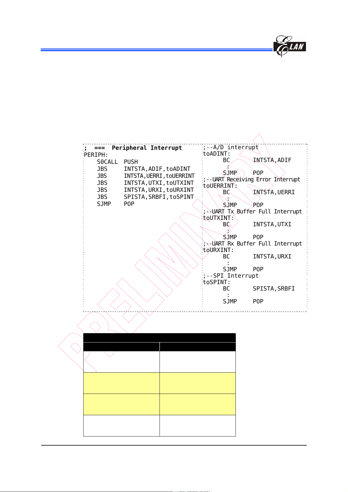
7.5.5 Peripheral Interrupt
1. A/D (Analog to Digital converter) Interrupt: A/D is used to convert analog input
2. UERRI Interrupt: UART receiving error interrupt
3. UTXI Interrupt: UART transfer buffer empty interrupt
4. URXI Interrupt: UART receiver buffer full interrupt
5. SRBFI Interrupt: SPI read buffer full interrupt
Code Example:
; === Peripheral Interrupt
PERIPH:
S0CALL PUSH
JBS INTSTA,ADIF,toADINT
JBS INTSTA,UERRI,toUERRINT
JBS INTSTA,UTXI,toUTXINT
JBS INTSTA,URXI,toURXINT
JBS SPISTA,SRBFI,toSPINT
SJMP POP
7.6 Progra m ROM Map
signal to digital output bits. When the conversion is completed,
an A/D interrupt occurs.
;--A/D interrupt
toADINT:
BC INTSTA,ADIF
:
SJMP POP
;--UART Receiving Error Interrupt
toUERRINT:
BC INTSTA,UERRI
:
SJMP POP
;--UART Tx Buffer Full Interrupt
toUTXINT:
BC INTSTA,UTXI
:
SJMP POP
;--UART Rx Buffer Full Interrupt
toURXINT:
BC INTSTA,URXI
:
SJMP POP
;--SPI Interrupt
toSPINT:
BC SPISTA,SRBFI
:
SJMP POP
8K Words × 2 Segments = 16K Words
Address Segment
0000h
|
000Bh
000Ch
|
0013h
0014h
|
001Fh
0020h
|
3FFFh
20 • Product Specification (V0.1) 10.11.2007
Interrupt Vector
(12 words)
Code Option
(8 words)
Test Program
(12 words)
Segment 0
|
Segment 1
(This specification is subject to change without further notice)
Page 27
EPH3600
RISC II Series Microcontroller
7.7 Data ROM Map
Maximum Size is 256K Words
Address
100000h
|
13FFFFh
Data ROM (4M bits)
7.8 RAM Map Register
(RAM Size: 128 Bytes + 32 Banks × 128 Bytes = 4224 Bytes)
7.8.1 Special and Control Register of RAM
Legend: R = Readable bit W = Writable bit – = unimplemented, read as “0”
Addr. Register Name Bit 7 Bit 6 Bit 5 Bit 4 Bit 3 Bit 2 Bit 1 Bit 0
0 INDF0
1 FSR0
2 PCL
3 PCM
Indirect Addressing Pointer 0
File Select Register 0 for INDF0
R/W R/W R/W R/W R/W R/W R/W R/W
PC7 PC6 PC5 PC4 PC3 PC2 PC1 PC0
R/W R/W R/W R/W R/W R/W R/W R/W
PC15 PC14 PC13 PC12 PC11 PC10 PC9 PC8
R/W
R/W
4 (Not Used) −
5 BSR
6 STKPTR
7 BSR1
8 INDF1
9 FSR1
A ACC
B TABPTRL
C TABPTRM
D TABPTRH
E CPUCON
R/W
− Bank Select Register for INDF0 & General RAM
R/W
Stack Pointer
R/W
− Bank Select Register 1 for INDF1
R/W
Indirect Addressing Pointer 1
R R/W
1 File Select Register 1 for INDF1
R/W
Accumulator
R/W
Table Pointer Low
R/W
Table Pointer Middle
R/W − R/W R/W R/W R/W R/W R/W
Table Pointer High
R/W R/W R/W R/W R/W R/W
PEN − − SMCAND SMIER GLINT MS1 MS0
Product Specification (V0.1) 10.11.2007 • 21
(This specification is subject to change without further notice)
Page 28
EPH3600
RISC II Series Microcontroller
(Continued)
Addr. Register Name Bit 7 Bit 6 Bit 5 Bit 4 Bit 3 Bit 2 Bit 1 Bit 0
F STATUS
10 TRL2
11 PRODL
12 PRODH
13 ADOTL
14 ADOTH
15 UARTTX
16 UARTRX
17 Port A
18 Port B
19 Port C
1A Port D
1B (Not Used) −
1C (Not Used) −
1D R1D
1E R1E
1
1
1F (Not Used) −
20 PFS
21 STBCON
22 INTCON
23 INTSTA
24 TRL0L
25 TRL0H
R R R/W R/W R/W R/W R/W R/W
/TO /PD SGE SLE OV Z DC C
R/W
Timer 2 Reload Register
R/W
Multiplier Product Low
R/W
Multiplier Product High
R/W R/W R/W R R
WDTEN − ADWKEN − − FSS ADOT1 ADOT0
R R R R R R R R
ADOT9 ADOT8 ADOT7 ADOT6 ADOT5 ADOT4 ADOT3 ADOT2
W W W W W W W W
TB7 TB6 TB5 TB4 TB3 TB2 TB1 TB0
R R R R R R R R
RB7 RB6 RB5 RB4 RB3 RB2 RB1 RB0
R R R R R R R R
A.7 A.6 A.5 A.4 A.3 A.2 A.1 A.0
R/W R/W R/W R/W R/W R/W R/W R/W
B.7 B.6 B.5 B.4 B.3 B.2 B.1 B.0
R/W R/W R/W R/W R/W R/W R/W R/W
C.7 C.6 C.5 C.4 C.3 C.2 C.1 C.0
R/W R/W R/W R/W R/W R/W R/W R/W
D.7 D.6 D.5 D.4 D.3 D.2 D.1 D.0
R/W R/W R/W R/W R/W R/W R/W R/W
R1D.7 R1D.6 R1D.5 R1D.4 R1D.3 R1D.2 R1D.1 R1D.0
R/W R/W R/W R/W R/W R/W R/W R/W
R1E.7 R1E.6 R1E.5 R1E.4 R1E.3 R1E.2 R1E.1 R1E.0
R/W
Target PLL Frequency Selection Register
R/W
UINVEN −
R/W R/W R/W R/W R/W R/W R/W R/W
CPIE ADIE URXIE UTXIE UERRIE TMR2IE TMR1IE TMR0IE
R/W R/W R/W R/W R/W R/W R/W R/W
CPIF ADIF URXI UTXI UERRI TMR2I TMR1I TMR0I
R/W
Timer 0 Reload Low Byte Register
R/W
Timer 0 Reload High Byte Register
22 • Product Specification (V0.1) 10.11.2007
(This specification is subject to change without further notice)
Page 29

EPH3600
RISC II Series Microcontroller
(Continued)
Addr. Register Name Bit 7 Bit 6 Bit 5 Bit 4 Bit 3 Bit 2 Bit 1 Bit 0
26 TRL1
27 TR01CON
28 TR2CON
29 TRLIR
2A ELCON
2B POST_ID
2C ADCON
2D PAINTEN
2E PAINTSTA
2F PAWAKE
30 UARTCON
31 UARTSTA
32 (Not Used) −
33 (Not Used) −
34 DCRB
35 DCRC
36 DCRDE
37 (Not Used) −
38 (Not Used) −
39 (Not Used) −
3A PBCON
3B PCCON
3C PLLF
3D TOCL
3E TOCH
3F SPICON
R/W R/W R/W R/W R/W R/W R/W R/W
T1WKEN T1EN T1PSR1 T1PSR0 IREN T0CS T0PSR1 T0PSR0
R/W R/W R/W R/W R/W R/W R/W R/W
IRPSR1 IRPSR0 T0FNEN1 T0FNEN0 T2EN T2CS T2PSR1 T2PSR0
R/W R/W R/W
ELTEN CKP ELTRL5~ELTRL0
R/W R/W R/W R/W
− − FSR1_ID FSR0_ID − − FSR1PE FSR0PE
R/W R/W R/W R R/W R/W R/W
DET VRS ADEN PIROB − CHS2 CHS1 CHS0
R/W R/W R/W R/W R/W R/W R/W R/W
PA7IE PA6IE PA5IE PA4IE PA3IE PA2IE PA1IE PA0IE
R/W R/W R/W R/W R/W R/W R/W R/W
PA7I PA6I PA5I PA4I PA3I PA2I PA1I PA0I
R/W R/W R/W R/W R/W R/W R/W R/W
WKEN7 WKEN6 WKEN5 WKEN4 WKEN3 WKEN2 WKEN1 WKEN0
W R/W R/W R/W R/W R/W R R/W
TB8 UMODE1 UMODE0 BRATE2 BRATE1 BRATE0 UTBE TXE
R R/W R/W R/W R/W R/W R R/W
RB8 EVEN PRE PRERR OVERR FMERR URBF RXE
R/W R/W R/W R/W R/W R/W R/W R/W
Bit7DC Bit6DC Bit5DC Bit4DC Bit3DC Bit2DC Bit1DC Bit0DC
R/W R/W R/W R/W R/W R/W R/W R/W
Bit7DC Bit6DC Bit5DC Bit4DC Bit3DC Bit2DC Bit1DC Bit0DC
R/W R/W R/W R/W
− DHNPU DLNPU DHNDC DLNDC
R/W R/W R/W R/W R/W R/W R/W R/W
Bit7PU Bit6PU Bit5PU Bit4PU Bit3PU Bit2PU Bit1PU Bit0PU
R/W R/W R/W R/W R/W R/W R/W R/W
Bit7PU Bit6PU Bit5PU Bit4PU Bit3PU Bit2PU Bit1PU Bit0PU
Timer 0 Counting Value Low Byte Register
Timer 0 Counting Value High Byte Register
R/W R/W R/W R/W R/W R/W R/W R/W
TLS1 TLS0 BRS2 BRS1 BRS0 EDS DORD SE
Timer 1 Reload Register
Actual PLL Frequency Value Register
R/W
R/W
IR Reload Register
R
R
R
Product Specification (V0.1) 10.11.2007 • 23
(This specification is subject to change without further notice)
Page 30

EPH3600
RISC II Series Microcontroller
(Continued)
Addr. Reg ister Name Bit 7 Bit 6 Bit 5 Bit 4 Bit 3 Bit 2 Bit 1 Bit 0
40 SPISTA
41 SPRL
42 SPRM
43 SPRH
44 SFCR
45 (Not Used) −
46 (Not Used) −
47 (Not Used) −
48 SPHDR
49 SPHTCON
4A SPHTRL
4B VOCON 2
4C TR1C
4D TR2C
4E ADCF
4F (Not Used) −
50 (Not Used) −
51 (Not Used) −
52 (Not Used) −
53 (Not Used) −
54 PAPUR 2
55 PACON 2
1
R1D, R1E are generated register RAM.
2
When the PAPUR register & DAC bit are enabled and effective, the following conditons occur:
a) Code option setting can use PAPUR register, SPHTPSR1~0, and DAC bit.
b) The KE, /R2EN, and Bit7PU bit of PACON can NOT be used.
Note that the code option setting is available only from the real chip but can NOT be simulated
with the PM board.
R/W R/W R/W R/W R/W R
− − SRBFIE SRBFI SPWKEN SMP DCOL RBF
R/W
Shift Register Low Byte of SPI
R/W
Shift Register Middle Byte of SPI
R/W
Shift Register High Byte of SPI
R/W R/W R/W R/W R/W R/W R/W R/W
AGMD2 AGMD1 AGMD0
WDTPRS1 WDTPRS0 SPHSB CSB1 CSB0
R/W
Speech Data Register
R/W R/W R/W R/W R/W R/W R/W R/W
SPHTPSR1 SPHTPSR
0
SPHTI SPHTIE SPHTEN
SPHTRLH2 SPHTRLH1 SPHTRLH
0
R/W
Speech Reload Register
R/W R/W R/W R/W R/W
VOEN DAC − − − VOL2 VOL1 VOL0
R
Timer 1 Counting Value Register
R
Timer 2 Counting Value Register
R/W
A/D Clock Factor Register
R/W R/W R/W R/W R/W R/W R/W R/W
Bit7PU0 Bit6PU0 Bit5PU0 Bit4PU0 Bit3PU0 Bit2PU0 Bit1PU0 Bit0PU0
R/W R/W R/W R/W
− Bit7PU /R2EN /R1EN KE
24 • Product Specification (V0.1) 10.11.2007
(This specification is subject to change without further notice)
Page 31

EPH3600
RISC II Series Microcontroller
7.8.2 Other Un-banked Register of RAM:
Address Un-banked
56h
|
7Fh
General Purpose RAM
7.8.3 Banked Register of RAM:(selected by BSR)
Address Bank 0 Bank 1 Bank 2 Bank 3 …….. Bank 31
80h
|
FFh
General
Purpose
RAM
General
Purpose
RAM
7.9 Special Register Description
STKPTR (R06h)
The stack level starts from the bottom going up (in a decreasing order), starting from
0FFh of Bank 31.
Stack is located at Bank 30 and 31 from Address FFh~80h. Initial top position of
stack pointer is located at 00h.
Bits 0~6 of STKPTR are used as address pointer from 80h ~ FFh
Bit 7=1 is used to select Bank 31
Bit 7=0 is used to select Bank 30
Each INT/CALL will stack two bytes address, total capacity is 128 levels.
PCL, PCM (R02h, R03h): Program Counter Register
Bit 15 … Bit 8 Bit 7 … Bit 0
PCM PCL
General
Purpose
RAM
General
Purpose
RAM
……..
General
Purpose
RAM
Generates up to 64K×16 on-chip ROM addresses at the relative programming
instruction codes.
“S0CALL” loads the low 12 bits of the PC (4K×16 ROM).
“SCALL” or ”SJUMP” loads the low 13 bits of the PC (8K×16 ROM).
“LCALL” or ”LJUMP” loads the full 16 bits of the PC (64K×16 ROM)
“ADD R2, A” or “ADC R2, A” allows a relative address to be added to the current PC.
The carry bit of R2 will automatically carry into PCM.
Product Specification (V0.1) 10.11.2007 • 25
(This specification is subject to change without further notice)
Page 32

EPH3600
RISC II Series Microcontroller
Code Example:
START: MOV A,entry
MOV number,a ;number <-- entry
LCALL Indirect_JUMP
AAA: ........
.......
Indirect_JUMP:
MOV A,number
ADD A,ACC ; A<-- 2*A
ADD PCL,A ; PCL<-- PCL+A
function_table:
LJMP function_address_1 ; number=0
LJMP function_address_2 ; number=1
LJMP function_address_3 ; number=2
LJMP function_address_4 ; number=3
LJMP function_address_5 ; number=4
LJMP function_address_6 ; number=5
LJMP function_address_7 ; number=6
.........
function_address_1:
........; Function 1 operation
........
RET ; PC will return to AAA label
ACC (R0Ah): Accumulator. Internal data transfer, or instruction operand holding
POST_ID (R2Bh): Post increase / decrease the control register
Bit 7 Bit 6 Bit 5 Bit 4 Bit 3 Bit 2 Bit 1 Bit 0
- - FSR1_ID FSR0_ID - - FSR1PE FSR0PE
Bit 0 (FSR0PE): Enable FSR0 post increase/decrease function. FSR0 will Not carry
into or borrow from BSR.
Bit 1 (FSR1PE): Enable FSR1 post increase/decrease function. FSR1 will carry into
or borrow from BSR1.
Bit 4 (FSR0_ID): Setting to 1 means auto increase, resetting to 0 means auto
decrease of FSR0.
Bit 5 (FSR1_ID): Setting to 1 means auto increase, resetting to 0 means auto
decrease of FSR1.
7.9.1 Indirect Addressing Pointer 0
BSR (R05h) determines which b ank is active (working bank) among the 32 banks
(Bank 0 ~ Bank 31).
FSR0 (R01h) is an address register for INDF0. You can select up to 256 bytes
(Address: 00 ~ 0FFh).
INDF0 (R00h) is not a physically implemented register.
26 • Product Specification (V0.1) 10.11.2007
(This specification is subject to change without further notice)
Page 33

EPH3600
RISC II Series Microcontroller
7.9.2 Indirect Addressing Pointer 1
BSR1 (R07h) is a bank register for INDF1. It cannot determines the working bank
for the general register.
FSR1 (R09h) is an address register for INDF1. You can select up to 128 bytes
(Address: 80 ~ 0FFh). Bit 7 of FSR1 is fixed to 1.
INDF1 (R08h) is not a physically implemented register.
Code Example:
Data transform Bank 0 to Bank 1:
MOV A,#00110011B ; Enable FSR0 & FSR1 post increase
MOV POST_ID,A
BANK #0 ; BSR = 0 working bank
MOV A,#1
MOV BSR1,A ; BSR1 = 1 is Bank 1
MOV A,#80H
MOV FSR0,A ; FSR0 = 80H
CLR FSR1 ; FSR1 = 80H
MOV A,#80H
RPT ACC
MOVRP INDF1,INDF0 ; Move 80H ~ 0FFH data to Bank 1
:
Linear addressing capability of INDF1 is shown below:
Auto Increase on FSR1
(Set FSR1PE=1,FSR1 ID=1)
FDh
FEh
FFh
File Register
BANK 3
:
:
88
99
AA
80h
81h
82h
BANK 4
BB
CC
DD
:
:
Instruction BSR1 FS R1 INDF1
MOV A,INDF1
MOV A,INDF1
MOV A,INDF1
:
(* FSR1 will carry into BSR1)
(*Bit 7 of FSR1is fixed to 1)
Auto Decrease on FSR1
(Set FSR1PE=1,FSR1 ID=0)
Instruction BSR1 FSR 1 INDF1
MOV A,INDF1
MOV A,INDF1
MOV A,INDF1
:
(* FSR1 will borrow from BSR1)
(*Bit 7 of FSR 1is fix ed to 1)
AAFF03
BB8004
CC8104
DD8204
ACC
00
AA
BB
CC
ACC
BB8004
AAFF03
99FE03
88FD03
00
BB
AA
99
Product Specification (V0.1) 10.11.2007 • 27
(This specification is subject to change without further notice)
Page 34

EPH3600
RISC II Series Microcontroller
Code Example:
;*******************************************
;* Const => Working bank setting
;* REG => Save or Recall register
;*******************************************
; ***** RAM stack macro
; *** Initial RAM stack
IniRAMsk MACRO #Const
MOV A,#Const
MOV BSR1,A
CLR FSR1
BS POST_ID,FSR1PE
ENDM
; *** Push RAM stack
PushRAM MACRO REG
BS POST_ID,FSR1_ID
MOVRP INDF1,REG
ENDM
; *** Pop RAM stack
PopRAM MACRO REG
BC POST_ID,FSR1_ID
MOVPR REG,INDF1
ENDM
; *** Main start program
Mstart:
:
:
IniRAMsk #29
:
:
MnLoop:
:
:
LJMP MnLoop
; *** Interrupt routine
IntSR:
PushRAM ACC
PushRAM Status
:
:
:
PopRAM Status
PopRAM ACC
RETI
TABPTRL, TABPTRM, TABPTRH (R0Bh, R0Ch, R0Dh): Table Pointer Re gister
Bit 23 Bit 22 … Bit 16 Bit15 … Bit 8 Bit 7 … Bit 0
- TABPTRH TABPTRM TABPTRL
Program ROM or Internal ROM address register:
Bit 23 is used to select the internal/external memory.
Bit 20 ~ Bit 1 are used to point the memory address.
Bit 0 is used to select the low byte or high byte of the pointed word (see
TBRD instruction).
Code Example:
; *** Program ROM
:
:
TBPTH #(PROMTabB*2)/10000H
TBPTM #(PROMTabB*2)/100H
TBPTL # PROMTabB*2
:
:
TBRD 0,ACC ; no change
TBRD 1,ACC ; auto-increase
TBRD 2,ACC ; auto-decrease
:
:
; *** Program ROM data
PROMTabB:
DB 0x00,0x01,0x02,0x03,0x04,0x05
DB 0x10,0x11,0x12,0x13,0x14,0x15
DB 0x20,0x21,0x22,0x23,0x24,0x25
; *** Internal data ROM
INCLUDE "DROM_I.hdr";to ROMConverter
:
:
TBPTL #_Data_l
TBPTM #_Data_m
TBPTH #_Data_h
:
:
TBRD 0,ACC ; no change
TBRD 1,ACC ; auto-increase
TBRD 2,ACC ; auto-decrease
:
28 • Product Specification (V0.1) 10.11.2007
(This specification is subject to change without further notice)
Page 35

PRODL, PRODH (R11h, R12h): An unsigned or signed 8 × 8 hardware multiplier
is included in the microcontroller. The result is stored into the
16 bits product register.
CPUCON (R0Eh): MCU Control Register
Bit 7 Bit 6 Bit 5 Bit 4 Bit 3 Bit 2 Bit 1 Bit 0
PEN - - SMCAND SMIER GLINT MS1 MS0
Bit 3 (SMIER): Signed or unsigned selection bit of the Multiplier. (ACC)
“0” : Multiplier is unsigned
“1” : Multiplier is signed
Bit 4 (SMCAND): Signed or unsigned selection bit of the Multiplicand.
(Constant or Register)
“0” : Multiplier is unsigned
“1” : Multiplier is signed
Code Example:
; *** Signed multiplier operation
; === PRODH:PRODL = A x REG
BS CPUCON,SMIER
BS CPUCON,SMCAND
MUL A,REG
EPH3600
RISC II Series Microcontroller
; *** Unsigned multiplier operation
; === PRODH:PRODL = A x #k
BC CPUCON,SMIER
BC CPUCON,SMCAND
MUL A,# 88
Port A (R17h): is a general input register
PAPUR (R54h): Pull-up Resistor Control of Port A
Bit 7 Bit 6 Bit 5 Bit 4 Bit 3 Bit 2 Bit 1 Bit 0
Bit7PU0 Bit6PU0 Bit5PU0 Bit4PU0 Bit3PU0 Bit2PU0 Bit1PU0 Bit0PU0
Bit 7 ~ Bit 0 (Bit 7PU7 ~ Bit 0PU0): Enable Port A R2 pull-up resistor.
“0” : Disable pull-up resistor
“1” : Enable pull up resistor
NOTE
1. When the PAPUR register & DAC bit are enabled and effective, the
following conditons occur:
a) Code option setting can use PAPUR register and DAC bit.
b) The KE, /R2EN, and Bit7PU bit of PACON can NOT be used.
2. The code option setting is available only from the real chip but
cannot be simulated with the PM board.
PACON (R55h): Port A Control Register
Bit 7 Bit 6 Bit 5 Bit 4 Bit 3 Bit 2 Bit 1 Bit 0
- - - - Bit7PU /R2EN /R1EN KE
Bit 0 (KE): Key input enable/disable control bit.
“0” : Disable Key input function
“1” : Enable Key input function.
Product Specification (V0.1) 10.11.2007 • 29
(This specification is subject to change without further notice)
Page 36

EPH3600
RISC II Series Microcontroller
Bit 1 (/R1EN): R1 pull-up resistor (small resistor) control bit.
“0” : Enable R1 pull-up resistor
“1” : Disable R1 pull-up resistor
Bit 2 (/R2EN): R2 pull-up resistor (large resistor) control bit.
Bit 3 (Bit 7PU): Enable Port A.7 pull-up resistor.
“0” : Disable pull-up resistor
“1” : Enable pull up resistor
PAINTEN (R2Dh): is Port A interrupt control register
“0” : Disable interrupt function
PAINTSTA (R2Eh): is Port A interrupt status register
Set to “1” when pin falling edge is detected
“0” : Enable R2 pull-up resisto r
“1” : Disable R2 pull-up resistor
“1” : Enable interrupt function
Clear to “0” by software
PAWAKE (R2Fh): is Port A wake-up control register
“0” : Disable wake-up function
“1” : Enable wake-up function
Port B (R18h) are general I/O registers
DCRB (R34h): Port B Direction Control
“0” : Output pin setting
“1” : Input pin setting
PBCON (R3Ah): Pull-up Resistor Control of Port B
“0” : Disable pull-up resistor
“1” : Enable pull-up resistor
Port C (R19h): are General I/O Registers
DCRC (R35h): Port C Direction Control
“0” : Output pin setting
“1” : Input pin setting
PCCON (R3Bh): Pull-up Resistor Control of Port C.
“0” : Disable pull-up resistor
“1” : Enable pull-up resistor
30 • Product Specification (V0.1) 10.11.2007
(This specification is subject to change without further notice)
Page 37

Port D (R1Ah): is a General I/O Register
DCRDE (R36h): Direction Control & Pull-up Resistor Control of Port D
Bit 7 Bit 6 Bit 5 Bit 4 Bit 3 Bit 2 Bit 1 Bit 0
- - - - DHNPU DLNPU DHNDC DLNDC
Bit 1 (DHNDC) & Bit 0 (DLNDC): Port D high nibble direction control
“0” : Output pin setting
Bit 3 (DHNPU) & Bit 2 (DLNPU): Enable Port D high nibble pull-up resistor
“0” : Disable pull up resistor
Code Example:
; *** Port A function
; --- Port A interrupt
INPTINT:
PUSH
MOV A,PAINTSTA
BC PACON,KE
; --- Port A interrupt
JBS STATUS,F_Z,Q_PAINT
MOV PORTD,A
Q_PAINT:
POP
RETI
; --- Port A R2 pull-up enable
MOV A,#00001010B
MOV PACON,A
; --- Port A interrupt
MOV A,#11111111B
MOV PAINTEN,A
CLR PAINTSTA
; --- Port A wakeup
MOV PAWAKE,A
BS CPUCON,GLINT
; --- Sleep mode
BC CPUCON,MS1
KeyLoop:
BS PACON,KE
SLEP
NOP
:
SJMP KeyLoop
EPH3600
RISC II Series Microcontroller
“1” : Input pin setting
“1” : Enable pull-up resistor
; *** Output function => 0XAAh to all port
CLR DCRC
CLR DCRB
CLR DCRDE
MOV A,#0XAA
MOV PORTC,A
MOV PORTB,A
MOV PORTD,A
;
; *** Input function => Input port to RAM 80 ~ 83h
BS POST_ID,FSR1_ID
BS POST_ID,FSR1PE
CLR BSR1
CLR FSR1
MOV A,#00001011B
MOV PACON,A
MOV A,#0XFF
MOV DCRB,A
MOV PBCON,A
MOV DCRC,A
MOV PCCON,A
MOV DCRDE,A
MOVRP INDF1,PORTA
BC PACON,KE
MOVRP INDF1,PORTB
MOVRP INDF1,PORTC
MOVRP INDF1,PORTD
Product Specification (V0.1) 10.11.2007 • 31
(This specification is subject to change without further notice)
Page 38

EPH3600
RISC II Series Microcontroller
8 Peripheral
8.1 Timer 0 (16-bit Timer with Capture and Event Counter Functions)
TRL0H:TRL0L
Timer 0
(16-bit Counter)
AGMD2~0
Edge Detector
Comparator
Reset
Counting
Value
Selector
T0FNEN1~0
Timer 0 INT
T0CH:T0CL
CPIF
Fosc
FPLL/2
T0CS
T0PSR1~0
Fcs
Prescaler
EVIN/CPIN
T0FNEN1~0
Function
Enable
Selector
Schmit
Trigger
Figure 8-1 Timer 0 Function Block Diagram
8.1.1 Timer 0 Mode:
Under this mode, Timer 0 is used as a general-purpose 16-bit up counter. An
interrupt is available for user’s application.
A prescaler for the timer is also available. The T0PSR2~T0PSR0 bits of the
TR01CON register determine the prescaler ratio and generate different clock rates for
the timer clock source. Counter value will be incremented by one (counting up)
according to the timer clock source and stored into the T0CH: T0CL register. The
clock source (Fcs) is selected from Fosc or F
T0PSR1~0. When the counting value is larger than TRL0H: TRL0L value, Timer 0
interrupt will occur, and the counter value will be reset to zero automatically.
/2 by T0CS and pre-scaled by
PLL
1
T
()
10:0Pr
+××= LTRLHTRLescaler
Fcs
Timer 0 Frequency:
Clock Source Fper / 2 TRL0H:TRL0L Prescaler Timer 0 Freq.
Fosc (32.768kHz) - FFFFh 1:64 128Hz
Fpll (8MHz) 4MHz 00FFh 1:1 15.6kHz
Fpll (16MHz) 8MHz 00FFh 1:1 31.2kHz
32 • Product Specification (V0.1) 10.11.2007
(This specification is subject to change without further notice)
Page 39

EPH3600
RISC II Series Microcontroller
8.1.2 Capture Mode: CPIN (Port B.5) Pin
Capture is a function that captures a Timer 0 value when an event occurs on CPIN pin.
The counter value is captured at: 1st rising edge, 2nd falling edge, etc.; 1st falling
edge, 2nd rising edge, etc.; every rising edge or every falling edge selected by
AGMD2~0 bit of the SFCR register. When an event edge is detected from CPIN
input pin, the interrupt flag CPIF is set. If a new event edge is detected before the old
value in T0CH: T0CL register is read, the old captured value will be lost.
The CPIN pin should be configured in capture function input by setting T0FNEN1~0
bits of TR2CON register.
1
T 0:00:0Pr
Fcs
()()
[]
−××=
CLTCHTCLTCHTescaler
OLDNEW
Capture Mode Example:
T0FNEN1~0
AGMD2~0
T0CH:T0CL
00
000
CPIN
Timer0
P1 P2 P3 P4 P5P6P7 P8 P9
CPIF
P2 P6
001 010
P10 P11
P7 P9P3
10
011
P12 P13P14
P15
P11 P13 P15
P16 P17
100
P18 P19 P20
P17 P21
101
P21
P22 P23 P24 P25 P26 P27 P28 P29 P30
P22
P31 P32
P33
8.1.3 Event Counter Mode: EVIN (Port B.5) Pin
Event counter is a function wherein the 16-bit counter value increments by one when
an event occurs on EVIN pin at: every rising edge or every falling edge selected by
AGMD2~0 bit of the SFCR register. In other words, the Timer 0 clock source is from
an external event (EVIN pin).
The EVIN pin should be configured in event counting function input by setting the
T0FNEN1~0 bits of the TR2CON register. The counting value of Timer 0 will be
stored in T0CH: T0CL registers.
Event Counter Mode Example:
T0FNEN1~0
AGMD2~0
Timer 0
T0CH:T0CL
00 11
010 011
EVIN
P0 P1 P2 P3 P4 P5
P0 P1 P2 P3 P4 P5
Product Specification (V0.1) 10.11.2007 • 33
(This specification is subject to change without further notice)
Page 40

EPH3600
RISC II Series Microcontroller
TRL0H, TRL0L (R25h, R24h): is used to store the values that are compared with
T0CH, T0CL (R3Eh, R3Dh): is used to store the Timer 0 counting value in Timer
TR01CON (R27h): Timer 0 and Timer 1 Control Register
Bit 7 Bit 6 Bit 5 Bit 4 Bit 3 Bit 2 Bit 1 Bit 0
T1WKEN T1EN T1PSR1 T1PSR0 IREN T0CS T0PSR1 T0PSR0
Bit 1 ~ Bit 0 (T0PSR1~T0PSR0): Timer 0 Prescaler select bit
T0PSR1: T0PSR0 Prescaler Value
Bit 2 (T0CS): Timer 0 clock source select bit
Timer 0 register.
0 mode and Event counter mode. But in Capture
mode, it is used to store the captured value.
00 1:1
01 1:4
10 1:16
11 1:64
“0” : Clock source is from Fosc
“1” : Clock source is from F
PLL/2
TR2CON (R28h): Timer 2 Control Register
Bit 7 Bit 6 Bit 5 Bit 4 Bit 3 Bit 2 Bit 1 Bit 0
IRPSR1 IRPSR0 T0FNEN1 T0FNEN0 T2EN T2CS T2PSR1 T2PSR0
Bit 5 ~ Bit 4 (T0FNEN1 ~ T0FNEN0): Timer 0 and Capture, event counter mode
selection bits.
SFCR (R44h): Special Function Control Register
Bit 7 Bit 6 Bit 5 Bit 4 Bit 3 Bit 2 Bit 1 Bit 0
AGMD2 AGMD1 AGMD0 WDTPSR1 WDTPSR0 SPHSB CSB1 CSB0
Bit 7 ~ Bit 5 (AGMD2 ~ AGMD0): Capture and Event Counter function e dg e
detector selection bits.
T0FNEN 1 ~ 0 Mode AGMD 2~0 Edge Mode
00 Disable - 01 Timer 0 - -
000 1st Rising edge, 2nd falling edge, etc.
001 1st Falling edge, 2nd rising edge, etc.
10 Capture
11 Event Counter
010 Every rising edge
011 Every falling edge
100 Every 4th rising edge
101 Every 16th rising edge
010 Every rising edge
011 Every falling edge
Note: 1. When changing from one mode to another, the Timer 0 must be initially disabled.
2. To avoid error, setup T0FNEN1 and T0FNEN0 simultaneously.
34 • Product Specification (V0.1) 10.11.2007
(This specification is subject to change without further notice)
Page 41

EPH3600
RISC II Series Microcontroller
CPUCON (R0Eh): MCU Control Register
Bit 7 Bit 6 Bit 5 Bit 4 Bit 3 Bit 2 Bit 1 Bit 0
PEN - - SMCAND SMIER GLINT MS1 MS0
Bit 2 (GLINT): Global Interrupt Control Bit
“0” : Disable all interrupts
“1” : Enable all un-masked interrupt
INTCON (R22h): Interrupt Control Register
Bit 7 Bit 6 Bit 5 Bit 4 Bit 3 Bit 2 Bit 1 Bit 0
CPIE ADIE URXIE UTXIE UERRIE TMR2IE TMR1IE TMR0IE
Bit 0 (TMR0IE): Timer 0 Interrupt Control Bit
“0” : Disable Timer 0 interrupt
“1” : Enable Timer 0 interrupt
Bit 7 (CPIE): Capture Interrupt Control bit
“0” : Disable Capture interrupt
“1” : Enable Capture interrupt
INTSTA (R23h): Interrupt Status Register
Bit 7 Bit 6 Bit 5 Bit 4 Bit 3 Bit 2 Bit 1 Bit 0
CPIF ADIF URXI UTXI UERRI TMR2I TMR1I TMR0I
Bit 0 (TMR0I): Set to 1 when Timer 0 is larger than TRL0H ~ TRL0L value
Clear to 0 by software or Timer 0
Bit 7 (CPIF): Set to 1 when Capture input edge is detected
Clear to 0 by software or disable Capture
Code Example:
;===Timer 0 interrupt
TIMERINT:
PUSH
JBC INTSTA,TMR0I,Q_Time
BC INTSTA,TMR0I
BTG PORTC,3
Q_Time:
POP
RETI
;===Timer 0 = (8M/2) / [4 x 3FFF + 1]
Timer0SR:
:
System setting 8MHz
PC.2 Port C & D setting output port
:
; --- Fpll & Prescaler 1:4
;===Capture Input Interrupt
CAPINT:
PUSH
JBS INTSTA,CPIF,Q_ICAP
BC INTSTA,CPIF
BTG PORTC,3
BS INTFLAG,F_ICAP
Q_ICAP:
POP
RETI
;
;===1st falling edge,2nd rising edge, etc.
CAP_SR:
System setting 8MHz
PC.2 Port C & D setting output port
User setting F_ICAP flag.
Product Specification (V0.1) 10.11.2007 • 35
(This specification is subject to change without further notice)
Page 42

EPH3600
RISC II Series Microcontroller
MOV A,#00000101B
MOV TR01CON,A
; --- 4ms = (4 x 16383 + 1)/(8M/2)
MOV A,#0FFH
MOV TRL0L,A
MOV A,#03FH
MOV TRL0H,A
; --- Timer 0 mode
MOV A,#00010000B
MOV TR2CON,A
; --- Timer 0 interrupt enable
BS INTCON,TMR0IE
; --- Clear Timer 0 interrupt status.
BC INTSTA,TMR0I
; --- Enable global interrupt
BS CPUCON,GLINT
TimeLoop:
; --- Out Timer 0 count to Port C :D
MOVRP PORTC,T0CH
MOVRP PORTD,T0CL
SJMP TimeLoop
:
; --- Count end => 0FFFFH
MOV A,#0XFF
MOV TRL0H,A
MOV TRL0L,A
; --- PLL/2 & Prescaler 1:1
; --- (8MHz/2)/65536=61Hz
MOV A,#00000100B
MOV TR01CON,A
; --- 1st Falling - 2nd Rising
MOV A,#00100000B
MOV SFCR,A
BS INTCON,CPIE
; --- 10->Capture Enable
MOV A,#00100000B
MOV TR2CON,A
BC INTFLAG,F_ICAP
BS CPUCON,GLINT
CAP_LOOP:
JBC INTFLAG,F_ICAP,CAP_LOOP
BC INTFLAG,F_ICAP
; --- Out capture count to Port C :D
MOVRP PORTC,T0CH
MOVRP PORTD,T0CL
SJMP CAP_LOOP
; === Every rising edge
EVcntSR:
:
System setting 8MHz
Port C & D setting output port
:
MOV A,#0XFF ; Switch 256 times reload
MOV TRL0L,A
CLR TRL0H ; Count start 0000H
BS TR01CON,T0CS ; PLL/2
MOV A,#01000000B
MOV SFCR,A ; Rising edge
MOV A,#00110000B
MOV TR2CON,A ; 11->Event count Enable
EV_LOOP:
MOVRP PORTC,T0CH ; Out event count to Port C:D
MOVRP PORTD,T0CL
SJMP EV_LOOP
36 • Product Specification (V0.1) 10.11.2007
(This specification is subject to change without further notice)
Page 43

8.2 Timer 1 (8 Bits)
EPH3600
RISC II Series Microcontroller
TRL1
reload
PrescalerFosc
T1PSR1~0
underflow
Timer 1
Figure 8-2 Timer 1 Function Block Diagram
Timer 1 INT or
Timer 1 wake up
TR1C
Timer 1 is a general-purpose 8-bit down counter for applications requiring time
counting. Interrupt and wake up functions are offered for your application. The clock
source is from the oscillator clock.
A prescaler is also available for the timer. The T1PSR1~T1PSR0 bits of the
TR01CON register determine the prescaler ratio and generate different clock rates for
the timer clock source. Setting T1WKEN bit of the TR01CON register to 1 will enable
the Timer 1 underflow wake-up function in IDLE MODE.
Counting value will be decremented by one (count down) according to the real timer
clock source. When the counter underflows, the timer interrupt will be triggered if the
global interrupt and Timer 1 interrupt are both enabled. At the same time, the TRL1
value is automatically reloaded into the 8 bits counter.
1
T
()
11Pr
+××= TRLescaler
Focs
The Timer 1 frequency range is from 0.5Hz (TRL1 = 0FFh, prescaler = 1:256) to
8.192kHz (TRL1 = 0h, prescaler = 1:4). The clock source is from the oscillator clock
(Fosc).
TRL1 (R26h): Use to store the auto-reload value of Timer 1. When enabling
Timer 1 or an underflow occurs, TRL1 register value will
automatically be reloaded into the 8 bits counter.
TR1C (R4Ch): Use to store the Timer 1 Counting Value
Product Specification (V0.1) 10.11.2007 • 37
(This specification is subject to change without further notice)
Page 44

EPH3600
RISC II Series Microcontroller
TR01CON (R27h): Timer 0 and Timer 1 Control Register
Bit 7 Bit 6 Bit 5 Bit 4 Bit 3 Bit 2 Bit 1 Bit 0
T1WKEN T1EN T1PSR1 T1PSR0 IREN T0CS T0PSR1 T0PSR0
Bit 5 ~ Bit 4 (T1PSR1~T1PSR0): Timer 1 Pre-scale Select Bit.
Bit 6 (T1EN): Timer 1 Enable Control Bit
“0” : Disable Timer 1 (stop counting)
Bit 7 (T1WKEN): Enable bit of Timer 1 underflow wake-up function in IDLE MODE.
“0” : Disable Timer 1 wake-up function
T1PSR1: T1PSR0 Prescaler Value
00 1:4
01 1:16
10 1:64
11 1:256
“1” : Enable Timer 1
“1” : Enable Timer 1 wake-up function
CPUCON (R0Eh): MCU Control Register
Bit 7 Bit 6 Bit 5 Bit 4 Bit 3 Bit 2 Bit 1 Bit 0
PEN - - SMCAND SMIER GLINT MS1 MS0
Bit 2 (GLINT): Global Interrupt Control Bit
INTCON (R22h): Interrupt Control Register
Bit 7 Bit 6 Bit 5 Bit 4 Bit 3 Bit 2 Bit 1 Bit 0
CPIE ADIE URXIE UTXIE UERRIE TMR2IE TMR1IE TMR0IE
Bit 1 (TMR1IE): Timer 1 Interrupt Control Bit
“0” : Disable Timer 1 interrupt
“1” : Enable Timer 1 interrupt
INTSTA (R23h): Interrupt Status Register
Bit 7 Bit 6 Bit 5 Bit 4 Bit 3 Bit 2 Bit 1 Bit 0
CPIF ADIF URXI UTXI UERRI TMR2I TMR1I TMR0I
Bit 1 (TMR1I): Set to 1 when Timer 1 interrupt occurs
Clear to 0 by software or disable Timer 1
38 • Product Specification (V0.1) 10.11.2007
(This specification is subject to change without further notice)
Page 45

EPH3600
RISC II Series Microcontroller
Code Example:
; === Timer 1 interrupt
TIMERINT:
PUSH
JBC INTSTA,TMR1I,Q_Time
BC INTSTA,TMR1I
BTG PORTC,3
Q_Time:
POP
RETI
; === Timer 1 = 32.768K/[256 x 3F + 1]
Timer1SR:
:
PC.2 setting output port
:
MOV A,#10110000B
MOV TR01CON,A ; Fosc & Prescaler 1:256 & wakeup
MOV A,#03FH
MOV TRL1,A ; 0.5sec = (256 x 63 + 1)/32.768K
BS TR01CON,T1EN ; Timer 1 enable
BS INTCON,TMR1IE ; Timer 1 interrupt enable
BC INTSTA,TMR1I ; Clear Timer 1 interrupt status
BS CPUCON,GLINT ; Enable global interrupt
BS CPUCON,MS1 ; Idle mode
T1WLoop:
SLEP
NOP
:
SJMP T1Wloop
Product Specification (V0.1) 10.11.2007 • 39
(This specification is subject to change without further notice)
Page 46

EPH3600
RISC II Series Microcontroller
8.3 Timer 2 (8 Bits)
TRL2
reload
Fosc
FPLL/2
Fcs
Prescaler
T2PSR1~0T2CS
Figure 8-3 Timer 2 Function Block Diagram
Timer 2
T2EN
underflow
Timer 2 INT
TR2C
Timer 2 is a general-purpose 8-bit down counter for applications that require time
counting. Interrupt functions are available for your application. The clock source
(Fcs) is from the oscillator clock or F
PLL/2.
There is a prescaler for the timer. The T2PSR1~T2PSR0 bits of the TR2CON
register determine the prescaler ratio and generate different clock rates for the timer
clock source.
Counting value will be decremented by one (counting down) according to the timer
clock source. When the counter value underflows, a timer interrupt will occur (if
Timer 2 interrupt is enabled).
1
T
()
12Pr
+××= TRLescaler
Fcs
Timer 2 Frequency:
Clock Source Fper / 2 TRL2 Prescaler Timer 2 Freq.
Fosc (32.768kHz) - FFh 1:8 16Hz
Fpll (8MHz) 4MHz 0Fh 1:1 250kHz
Fpll (16MHz) 8MHz 0Fh 1:1 500kHz
TRL2 (R10h): is used to store the auto-reload value of Timer 2. When enabling
Timer 2 or an underflow occurs, TRL2 register will automatically be
reloaded into the 8 bits counter.
TR2C (R4Dh): is used to store the Timer 2 counting value
40 • Product Specification (V0.1) 10.11.2007
(This specification is subject to change without further notice)
Page 47

EPH3600
RISC II Series Microcontroller
TR2CON (R28h): Timer 2 Control Register
Bit 7 Bit 6 Bit 5 Bit 4 Bit 3 Bit 2 Bit 1 Bit 0
IRPSR1 IRPSR0 T0FNEN1 T0FNEN0 T2EN T2CS T2PSR1 T2PSR0
Bit 1 ~ Bit 0 (T2PSR1~T2PSR0): Timer 2 Prescaler select bit.
T2PSR1: T2PSR0 Prescaler Value
00 1:1
01 1:2
10 1:4
11 1:8
Bit 2 (T2CS): Timer 2 Clock Source Select Bi t
“0” : Clock source is from Fosc
“1” : Clock source is from FPLL/2
Bit 3 (T2EN): Timer 2 Enable Control Bit
“0” : Disable Timer 2 (stop counting)
“1” : Enable Timer 2
CPUCON (R0Eh): MCU Control Register
Bit 7 Bit 6 Bit 5 Bit 4 Bit 3 Bit 2 Bit 1 Bit 0
PEN - - SMCAND SMIER GLINT MS1 MS0
Bit 2 (GLINT): Global Interrupt Control Bit
INTCON (R22h): Interrupt Control Register
Bit 7 Bit 6 Bit 5 Bit 4 Bit 3 Bit 2 Bit 1 Bit 0
CPIE ADIE URXIE UTXIE UERRIE TMR2IE TMR1IE TMR0IE
Bit 2 (TMR2IE): Timer 2 Interrupt Control bit
“0” : Disable Timer 2 interrupt
“1” : Enable Timer 2 interrupt
INTSTA (R23h): Interrupt Status Register
Bit 7 Bit 6 Bit 5 Bit 4 Bit 3 Bit 2 Bit 1 Bit 0
CPIF ADIF URXI UTXI UERRI TMR2I TMR1I TMR0I
Bit 2 (TMR2I): Set to 1 when Timer 2 interrupt occurs
Clear to 0 by software or disable Timer 2
Product Specification (V0.1) 10.11.2007 • 41
(This specification is subject to change without further notice)
Page 48

EPH3600
RISC II Series Microcontroller
Code Example:
; === Timer 2 interrupt
TIMERINT:
PUSH
JBC INTSTA,TMR2I,Q_Time
BC INTSTA,TMR2I
BTG PORTC,3
Q_Time:
POP
RETI
; === Timer 2 = (8M/2)/[4 x 3F + 1]
Timer2SR:
:
System setting 8MHz
Port D setting output port
:
MOV A,#00000110B
MOV TR2CON,A ; Fpll & Prescaler 1:4
MOV A,#03FH
MOV TRL2,A ; 16us = (4 x 63 + 1)/(8M/2)
BS TR2CON,T2EN ; Timer 2 enable
BS INTCON,TMR2IE ; Timer 2 interrupt enable
BC INTSTA,TMR2I ; Clear Timer 2 interrupt status
BS CPUCON,GLINT ; Enable global interrupt
TMR2Loop:
MOVRP PORTD,TR2C ; Out Timer 2 count to Port D
SJMP TMR2Loop
42 • Product Specification (V0.1) 10.11.2007
(This specification is subject to change without further notice)
Page 49

8.4 IR Generator: IROT (Port B.2) Pin
EPH3600
RISC II Series Microcontroller
TRLIR
reload
PrescalerFPLL
IRP SR 1 ~ 0
8-bit C ounter
IRE N
Figure 8-4 IR Generator Function Block Diagram
underflow
Divide
by 2
IROT
IR function is enabled by IREN bit and output on the IROT (Port B.2) pin by a
general-purpose 8-bit down counter. When IREN is low, the T-flip-flop should be
initialized, as IROT equals zero. The clock source is from the PLL clock. The
IRPSR1 ~ IRPSR0 bits of the TR2CON register determine the prescaler ratio and
generate different clock rates for the timer clock source. The counting value will be
decremented by one (counting down) according to the clock source. When the
counter value underflows, the IR reload register value will be reloaded into the
counter.
T
2
F
PLL
()
1Pr
+××= TRLIRescaler
IR Carrier Signal Frequency:
Clock Source Fper / 2 TRLIR Prescaler IR Freq.
Fpll (8MHz) 4MHz 0Fh 1:1 250kHz
Fpll (16MHz) 8MHz 0Fh 1:1 500kHz
TRLIR (R29h): is used to store the auto-reload value of the IR gene rator. When
enabling the IR generator or when an underflow occurs, the TRLIR
register value is automatically reloaded into the 8 bits counter.
TR01CON (R27h): Timer 0 and Timer 1 Control Register
Bit 7 Bit 6 Bit 5 Bit 4 Bit 3 Bit 2 Bit 1 Bit 0
T1WKEN T1EN T1PSR1 T1PSR0 IREN T0CS T0PSR1 T0PSR0
Bit 3 (IREN): IR function enable control bit
“0” : Disable IR function and recover IROT pin as a general I/O pin
“1” : Enable IR function and change Port B.2 as IROT output pin.
Product Specification (V0.1) 10.11.2007 • 43
(This specification is subject to change without further notice)
Page 50

EPH3600
RISC II Series Microcontroller
TR2CON (R28h): Timer 2 Control Register
Bit 7 Bit 6 Bit 5 Bit 4 Bit 3 Bit 2 Bit 1 Bit 0
IRPSR1 IRPSR0 T0FNEN1 T0FNEN0 T2EN T2CS T2PSR1 T2PSR0
Bit 7 ~ Bit 6 (IRPSR1~IRPSR0): IR Generator Prescaler Select Bit
Code Example:
; === IR generator 31kHz
:
System setting 10MHz
:
MOV A,#10000000B
MOV TR2CON,A ; Prescaler 1: 16
MOV A,#9
MOV TRLIR,A ; 10MHz /[ 2 x 16 x ( 9 + 1 ) ] = 31kHz
BS TR01CON,IREN
IR_Loop:
SJMP IR_Loop
IRPSR1: IRPSR0 Prescaler Value
00 1:1
01 1:4
10 1:16
11 1:64
8.5 EL Timer (6 Bits)
ELTEN ELTRL5:0
reload
Fsystem/2
6 bit Counter
(EL Timer)
Figure 8-5 EL or IR Generator Timer Function Block Diagram
EL Timer is a 6-bit down counter that is suitable for counting the CHOP signal output.
The clock source is from 1/2 system cl ock (1MHz ~ 16MHz).
Counter value decreases (count down) by one according to the timer clock source.
When under flow occurs, the CHOP output level will be toggled. When EL timer is
enabled or underflow happens, ELTRL will automatically reload into 6-bit counte r.
underflow
÷ 2
256 Hz
Carrier
128 Hz
CKP
CHOP output (Port B.4)
CHOP output(Port B.5)
CK output (Port B.3)
CK output(Port B.4)
44 • Product Specification (V0.1) 10.11.2007
(This specification is subject to change without further notice)
Page 51

EPH3600
RISC II Series Microcontroller
ELTEN bit is used to enable EL timer and change Port B.4 and Port B.3 to CHOP
and CK output pin.
Where: CHOP (Port B.4): Chop output pin of EL driver
CK (Port B.3): CK output pin of EL driver
CKP bit is used to select clock polarity of CHOP output (see timing diagram in
Figure 8-6 for further details).
The frequency range of CHOP carrier signal is from 128Hz (System clock at
32768Hz, ELTRL=3Fh) to 4MHz (System clock at 16MHz, ELTRL=0h).
)(Fsystem/2Fchop ×
×=
1
+
EL Code Option: EL Output Timing
Select “CHOP output is from carrier gating with 128Hz and CKP”
or “CHOP output is directly from carrier” (for IR function)
ELCON (R37h): EL control register
Bit 7 Bit 6 Bit 5 Bit 4 Bit 3 Bit 2 Bit 1 Bit 0
ELTEN CKP ELTRL5 ELTRL4 ELTRL3 ELTRL2 ELTRL1 ELTRL0
Bit5 ~ Bit0 (ELTRL5~ELTRL0): Store the auto reload value of EL timer. When EL
timer is enabled or underflow occurs, ELTRL5 ~ 0 will automatically
reload into 6-bit counter.
Bit6 (CKP): EL clock polarity select bit
“0” Idle state for CHOP pin is low level
“1” Idle state for CHOP pin is high level
Bit7 (ELTEN): EL/IR Timer enable control bit
“0” Disable EL Timer (stop counting) and recover CK and CHOP pin
to general I/O pin
1
2
1)(ELTRL
“1” Enable EL Timer and change Port B.3 and Port B.4 to CK and
CHOP output pin
Product Specification (V0.1) 10.11.2007 • 45
(This specification is subject to change without further notice)
Page 52

EPH3600
RISC II Series Microcontroller
8.5.1 EL Generator Timing
256H z
(internal clock)
128Hz
(internal clock)
Tdelay3
3.9ms
3.9ms
CHOP
(CKP = 0 )
3.9ms
3.9ms
Carrier
CHOP
(C K P = 1 )
1.95ms
5.85ms
Carrier
CK
Figure 8-6 EL Generator Timing Diagram
Code Example:
EL code option -- EL Output Timing:
Select “CHOP output is from carrier gating with 128Hz and CKP”
; === EL generator 200KHz
:
System setting 4MHz
:
MOV A,#00000100B
MOV ELCON,A ; (4MHz/2) / [(4+1) x 2] = 200KHz
BS ELCON,ELTEN ; Enable EL generator.
:
EL code option -- EL Output Timing:
Select “CHOP output is directly from carrier”.
; === EL generator 32.25KHz
:
System setting 8MHz
:
MOV A,#00111111B
MOV ELCON,A ; (8MHz/2) / [(63+1)x2] = 31.25KHz
BS ELCON,ELTEN ; Enable IR generator.
:
46 • Product Specification (V0.1) 10.11.2007
(This specification is subject to change without further notice)
Page 53

8.6 Watchdog Timer (WDT)
EPH3600
RISC II Series Microcontroller
Fosc/2 except @
SLEEP mode
Intern a l R C OS C
@ SLEEP mode
(16kHz +/- 20%)
FWDT
MUX Prescaler
Enable
MCU mode
2
WDTPSR1~0 WDTEN
Instruction "WDTC"
reset
8-bit Counter
(W D T )
overflow
W DT Time out reset
Figure 8-7 Watchdog Timer Function Block Diagram
The Watchdog Timer (WDT) clock source is from on -chip RC oscillator (16kHz ±
20%, MCU in Sleep mode) or F
will keep on running even when the oscillator has been turned off (i.e., in Sleep
Mode). WDT time-out will cause the MCU to reset (if WDT is enabled). To prevent
reset from occuring, you must clear the WDT value by using the “WDTC” instruction
before WDT time-out. Setting the WDTEN bit will enable the WDT function. The
WDT default condition is disabled A prescaler is also available to generate different
clock rates for the WDT clock source. The prescaler ratio is defined by WDTPSR1 ~
WDTPSR0.
T
/2 (MCU in Fast, Slow, or Idle mode). The WDT
OSC
F
1
WDT
()
1Pr
+××= WDTescaler
The WDT time out range is 64ms (prescaler = 1:4) to 2.048 second (prescaler = 1:128).
ADOTL (R13h): A/D Output Data Low Byte Register
Bit 7 Bit 6 Bit 5 Bit 4 Bit 3 Bit 2 Bit 1 Bit 0
WDTEN - ADWKEN - - FSS ADOT1 ADOT0
Bit 7 (WDTEN): Watchdog Timer enable bit.
“0” : Disable Watchdog Timer (stop running)
“1” : Enable Watchdog Timer
SFCR (R44h): Special Function Control Register
Bit 7 Bit 6 Bit 5 Bit 4 Bit 3 Bit 2 Bit 1 Bit 0
AGMD2 AGMD1 AGMD0 WDTPSR1 WDTPSR0 SPHSB CSB1 CSB0
Bit 4 ~ Bit 3 (WDTPSR1~WDTPSR0): Watchdog Timer Prescale r select bit
WDTPSR1: WDTPSR0 Prescaler Value
00 1:4
01 1:16
10 1:64
11 1:128
Product Specification (V0.1) 10.11.2007 • 47
(This specification is subject to change without further notice)
Page 54

EPH3600
RISC II Series Microcontroller
Code Example:
; === WDT setting 2.048sec
:
Timer 1 (0.5sec wakeup)
:
BS SFCR,WDTPSR0
BS SFCR,WDTPSR1 ; Prescaler 1:128
BC CPUCON,MS1 ; Change to sleep mode
WDTC
SLEP
WDT_Loop:
SJMP WDT_Loop
; === Timer 1 interrupt 0.5 sec
TIMERINT:
PUSH
JBC INTSTA,TMR1I,Q_Time
BC INTSTA,TMR1I
WDTC
:
:
Q_Time:
POP
RETI
8.7 Universal Asynchronous Receiver Transmitter (UART)
RS232C compatible
Mode selectable (7/8/9-bit) with/without parity bit
Baud rate selectable
Error detect function
Interrupt available for Tx buffer empty, Rx buffer full and receiver error
TXD and RXD port inverse output control
Timer0/32
RXD
Selector
Fsystem
RXE TXE
UINVEN
RB8
RX Control TX Control
RX s h ift re g iste r
UAR T R x reg. UARTTx reg.
Baud rate
generator
Parity con tro l
Interrupt
Control
Error flag
TB8
TXD
Data Bus
Figure 8-8 UART Function Block Diagram
UINVEN
48 • Product Specification (V0.1) 10.11.2007
(This specification is subject to change without further notice)
Page 55

EPH3600
RISC II Series Microcontroller
In Universal Asynchronous Receiver Transmitter (UART), each transmitted or
received character is individually synchronized by framing it with a start bit and stop
bit.
Full duplex data transfer is possible because the UART has independent transmit and
receive sections. Double buffering in both sections enables the UART to be
programmed for continuous data transfer.
The figure below shows the general format of one character sent or received. The
communication channel is normally held in the marked state (high). Character
transmission or reception starts with a transition to the space state (low).
The first bit transmitted or received is the start bit (low). It is followed by the data bits,
in which the least significant bit (LSB) comes first. The data bits are followed by the
parity bit. If present, then the stop bit or bits (high) confirm the end of the frame.
In receiving, the UART synchronizes on the falling edge of the start bit. When two or
more “0”s are detected during three sampling, it is recognized as a normal start bit
and receiving operation is started.
8.7.1 Data Format in UART
Idle state
START
bit
1 bit 7 or 8 bits
D0 D1 D2 Dn
One character or frame
Figure 8-9 UART Data Format Diagram
Parity
STOP
bit
bit
1 bit 1 bits
(mark)
8.7.2 UART Modes
There are three modes in UART. Mode 1 (7 bits data) and Mode 2 (8 bits data) allow
the addition of a parity bit. The parity bit addition is not available in Mode 3. The
Figure below shows the data format in each mode.
Product Specification (V0.1) 10.11.2007 • 49
(This specification is subject to change without further notice)
Page 56

EPH3600
RISC II Series Microcontroller
12345 11109876
START
START
START
START
START
7 bits DATA
7 bits DATA Parity
8 bits DATA
8 bits DATA Parity
9 bits DATA
STOP
STOP
STOP
STOP
STOP
Mode 1
Mode 2
Mode 3
UMODE PRE
0 0 0
0 0 1
0 1 0
0 1 1
1 0 X
Figure 8-10 UART Modes Data Format
8.7.3 UART Transmit Data
In transmitting serial data, the UART operates as follows:
1. Set the TXE bit of the UARTCON register to enable UART transmission function.
2. Write data into the UARTTX register, and the TBE bit of the UARTCON register
will be set by hardware. Then start transmitting.
3. Serially transmitted data are transmitted in the following order from the TXD pin:
(a) Start bit: one “0” bit is output
(b) Transmit data: 7, 8, or 9 bits data are output from LSB to MSB
(c) Parity bit: one parity bit (odd or even sele ctable) is output
(d) Stop bit: one “1” bit (stop bit) is outp ut
(e) Mark state: output “1” continues until the start bit of the next transmit data
4. After transmitting the stop bit, the UART generates a UTXI interrupt (if enabled)
8.7.4 UART Receive Data
1. Sets the RXE bit of the UARTCON register to enable the UART receiving
function.
2. The UART monitors the RXD pin and synchronizes internally when it detects a
start bit.
3. Received data is shifted into the UARTRX register in LSB to MSB sequence.
4. The parity bit and the stop bit are received. After one character is received, the
UART generates a URXI interrupt (if enabled). And the URBF bit of the
UARTSTA register is set to 1.
50 • Product Specification (V0.1) 10.11.2007
(This specification is subject to change without further notice)
Page 57

EPH3600
RISC II Series Microcontroller
5. The UART makes the following checks:
a) Parity check: The number of “1” in the receive data must match with the
even or odd parity setting of the EVEN bit in the UARTSTA
register.
b) Frame check: The start bit must be “0” and the stop bit must be “1.”
c) Overrun check: the URBF bit of the UARTCON register must be cleared
(i.e., the UARTRX register should be read out) before the
next received data are loaded into the UARTRX register.
If any of the checks failed, the UERRI interrupt will be generated (if enabled).
And the error flag is indicated in PRERR, OVERR or FMERR bit. The error flag
should be cleared by software, otherwise, a UERRI interrupt will occur when the
next byte is received.
6. Read the received data from the UARTRX register. The URBF bit will be cleared
by hardware.
8.7.5 UART Baud Rate Generator
The baud rate generator comprises of a circuit that generates a clock pulse
which determines the transfer speed of the transmitted/received data in the
UART.
The input clock of the baud rate generator is derived from the syst em clock
divided by 64 or from Timer 0 divided by 32.
The system clock should be at 9.83MHz (PFS = 150) or 14.745MHz
(PFS = 225) when UART is enabled.
The BRATE2 ~ BRATE0 bits of the UARTCON register determines the desired
baud rate.
8.7.6 UART Applicable Registers
UARTCON (R30h): UART Control Register
Bit 7 Bit 6 Bit 5 Bit 4 Bit 3 Bit 2 Bit 1 Bit 0
TB8 UMODE1 UMODE0 BRATE2 BRATE1 BRATE0 UTBE TXE
Bit 0 (TXE): Enables transmit data function
Bit 1 (UTBE): UART transfer buffer empty flag. Set to “1” when the transfer buffer is
empty. Reset to “0” automatically when writing into the UARTTX
register.
NOTE
When transmit data is enabled, the UTBE (read-only) bit will be
cleared by hardware. Hence, writing to the UARTTX register is
required when you want to start transmitting data.
Product Specification (V0.1) 10.11.2007 • 51
(This specification is subject to change without further notice)
Page 58

EPH3600
RISC II Series Microcontroller
Bit 4 ~ Bit 2 (BRATE 2 ~ 0): Baud Rate Selector
SELBR3 (for Code Option) 0: Fper = Fpll 1: Fper = Fpll x 2/3
BRATE2 ~ 0
000 Timer 0/32 Timer 0/32 Timer 0/32 Timer 0/32
001 Fper/4096 baud 2400 baud 3600 baud 2400 baud
010 Fper/2048 baud 4800 baud 7200 baud 4800 baud
011 Fper/1024 baud 9600 baud 14400 baud 9600 baud
100 Fper/512 baud 19200 baud 28800 baud 19200 baud
101 Fper/256 baud 38400 baud 57600 baud 38400 baud
110 Fper/128 baud 76800 baud 115200 baud 76800 baud
111 Fper/64 baud 153600 baud 230400 baud 153600 baud
Bit 6 ~ Bit 5 (UMODE 1 ~ 0): UART Mode
(PFS = 4 ~ 255)
Fpll
UMODE 1: UMODE 0 UART Mode
00 Mode 1: 7-bit data
01 Mode 2: 8-bit data
10 Mode 3: 9-bit data
11 Reserved
Fpll = 9.83MHz
(PFS = 150)
Fpll = 14.745MHz
(PFS = 225)
Fpll = 14.745MHz
(PFS = 225)
Bit 7 (TB8): Transmission Data Bit 8
UARTSTA (R31h): UART Status Register
Bit 7 Bit 6 Bit 5 Bit 4 Bit 3 Bit 2 Bit 1 Bit 0
RB8 EVEN PRE PRERR OVERR FMERR URBF RXE
Bit 0 (RXE): Enable receive data function
Bit 1 (URBF): UART read buffer full flag. Set to 1 when one character is received.
Reset to 0 automatically when read from the UARTRX register.
NOTE
When receive data is enabled, URBF (read-only) bit will be cleared by
hardware. Hence, reading from the UARTRX register is required to
avoid overrun error.
Bit 2 (FMERR): Framing error flag. Set to 1 when framing error occurs
Clear to 0 by software
Bit 3 (OVERR): Overrun error flag. Set to 1 when overrun error occurs
Clear to 0 by software
Bit 4 (PRERR): Parity error flag. Set to 1 when parity error occurs
Clear to 0 by software
52 • Product Specification (V0.1) 10.11.2007
(This specification is subject to change without further notice)
Page 59

EPH3600
RISC II Series Microcontroller
Bit 5 (PRE): Enable parity addition
“0” : Disable
“1” : Enable
Bit 6 (EVEN): Select parity check
“0” : Odd parity
“1” : Even parity
Bit 7 (RB8): Receiving Data Bit 8
UARTTX (R15h): UART Transfer Register
Bit 7 Bit 6 Bit 5 Bit 4 Bit 3 Bit 2 Bit 1 Bit 0
TB7 TB6 TB5 TB4 TB3 TB2 TB1 TB0
Bit 7 ~ Bit 0 (TB7 ~ TB0): Transmit data register. UARTTX register is write-only.
UARTRX (R16h): UART Receiver Register
Bit 7 Bit 6 Bit 5 Bit 4 Bit 3 Bit 2 Bit 1 Bit 0
RB7 RB6 RB5 RB4 RB3 RB2 RB1 RB0
Bit 7 ~ Bit 0 (RB7 ~ RB0): Receive data register. UARTRX regi ster is read-only.
STBCON (R21h): Strobe Output Control Register
Bit 7 Bit 6 Bit 5 Bit 4 Bit 3 Bit 2 Bit 1 Bit 0
UINVEN /REN BitST ALL STB3 STB2 STB1 STB0
Bit 7 (UINVEN): Enable UART TXD and RXD port inverse output.
“0” : Disable TXD and RXD port inverse output.
“1” : Enable TXD and RXD port inverse output.
CPUCON (R0Eh): MCU Control Register
Bit 7 Bit 6 Bit 5 Bit 4 Bit 3 Bit 2 Bit 1 Bit 0
PEN - - SMCAND SMIER GLINT MS1 MS0
Bit 2 (GLINT): Global Interrupt Control Bit
“0” : Disable all interrupts
“1” : Enable all un-masked interrupt
Product Specification (V0.1) 10.11.2007 • 53
(This specification is subject to change without further notice)
Page 60

EPH3600
RISC II Series Microcontroller
INTCON (R22h): Interrupt Control Register
Bit 7 Bit 6 Bit 5 Bit 4 Bit 3 Bit 2 Bit 1 Bit 0
CPIE ADIE URXIE UTXIE UERRIE TMR2IE TMR1IE TMR0IE
Bit 3 (UERRIE): Control bit of UART receiving error interrupt
“0” : Disable
Bit 4 (UTXIE): Control bit of UART Transfer buffer empty interrupt
“0” : Disable
Bit 5 (URXIE): Control bit of UART Receiver buffer full interrupt
“0” : Disable
INTSTA (R23h): Interrupt Status Register
Bit 7 Bit 6 Bit 5 Bit 4 Bit 3 Bit 2 Bit 1 Bit 0
CPIF ADIF URXI UTXI UERRI TMR2I TMR1I TMR0I
“1” : Enable
“1” : Enable
“1” : Enable
Bit 3 (UERRI): Set to 1 when UART receiving error occurs
Clear to 0 by software or disable UART
Bit 4 (UTXI): Set to 1 when UART transfer buffer empty occurs
Clear to 0 by software or disable UARTTX (TXE=0)
Bit 5 (URXI): Set to 1 when UART receiver buffer full occurs
Clear to 0 by software or disable UARTRX (RXE=0)
8.7.7 Transmit Counter Timing
1 2 3 4 5 6 7 8 9 1 0 1 1 12 13 1 4 1 5 16 1 2 3 4
/16
T
SYSTEM
One bit cycle
TXD pin
Start bit
Bit 0
Figure 8-11 UART Transmit Counter Timing
8.7.8 UART Transmit Operation (8-Bit Data with Parity Bit)
TXD
pin
UTBE
UTXI
START
D0 D1 D2 Dn
bit
Parity
bit
STOP
bit
START
D0 D1 D2
bit
Clear by hardware when
write d ata in to U A R T T x .
An d s ta rt tr a n sm ittin g .
Clear by
softw are
Figure 8-12 UART Transmit Operation
54 • Product Specification (V0.1) 10.11.2007
(This specification is subject to change without further notice)
Page 61

EPH3600
RISC II Series Microcontroller
Code Example:
; === UART Transfer buffer empty interrupt
PERIPH:
PUSH
JBC INTSTA,UTXI,Q_UTXINT
BC INTSTA,UTXI
MOV A,UTX_NO
COMA ACC
MOV UTX_NO,A
MOV UARTTX,A ; Tx data 55,AA,55,AA
Q_UTXINT:
POP
RETI
; === UART 38400 baud 8bit inverse
UTX_SR:
:
System setting 9.83MHz
:
BS STBCON,UINVEN ; TXD & RXD inverse
MOV A,#00110101B ; Enable Tx
MOV UARTCON,A ; 8bit, 38400baud
MOV A,#01100000B ; Disable Rx
MOV UARTSTA,A ; Even Parity
BC INTSTA,UTXI ; TX buffer empty occurs
BS INTCON,UTXIE ; En. TX interrupt
BS CPUCON,GLINT ; Global interrupt
MOV A,#0X55
MOV UTX_NO,A
MOV UARTTX,A ; Tx data 55
TX_loop:
SJMP TX_loop
8.7.9 Receive Counter Timing
Synchronization
(Reset counter)
1 2 3 4 5 6 7 8 9 10 11 12 13 14 15 16 1 2 3 4
12 13
/16
T
SYSTEM
RXD pin
Sampling
Timing
Product Specification (V0.1) 10.11.2007 • 55
(This specification is subject to change without further notice)
Stop bit
Start bit
Figure 8-13 UART Receive Counter Timing
One bit cycle
Bit 0
Page 62

EPH3600
RISC II Series Microcontroller
8.7.10 UART Receive Operation (8 bits da ta with parity and s top b it)
STAR T
RXD
pin
Sample
Timing
URBF
URXI
PRER R
OVERR
FM ERR
Sy nc h ro n iz atio n
D0 D1 D2 Dn
bit
Figure 8-14 UART Receive Operation
Code Example:
;===UART Receiver buffer full interrupt
PERIPH:
PUSH
JBC INTSTA,URXI,UERRINT
BC INTSTA,URXI
MOVPR URX_NO,UARTRX
SJMP Q_RXINT
;
;===UART error interrupt
UERRINT:
JBC INTSTA,UERRI,Q_RXINT
BC INTSTA,UERRI
;---Framing error flag
;---Over run error flag
;---Parity error flag
MOV A,UARTSTA
AND A,#00011100B
MOV PORTD,A
BC UARTSTA,FMERR
BC UARTSTA,OVERR
BC UARTSTA,PRERR
Q_RXINT:
POP
RETI
;===UART 38400 baud 8bit inverse
URX_SR:
:
System setting 9.83MHz
Port C & D setting output port
:
;---TXD & RXD inverse
BS STBCON,UINVEN
;---Disable Tx, 8bit, 38400baud
MOV A,#00110100B
MOV UARTCON,A
;---Enable Rx, Even Parity
MOV A,#01100001B
MOV UARTSTA,A
;---UART RX buffer empty interrupt
BS INTSTA,URXI
BS INTCON,URXIE
;---UART RX error interrupt
BS INTSTA,UERRI
BS INTCON,UERRIE
;---Global interrupt
BS CPUCON,GLINT
RX_loop:
MOVRP PORTC,URX_NO
SJMP RX_loop
Parity
bit
STOP
bit
START
bit
D0 D1 D2
Clear b y h ard w a re w h en
read d ata fro m U A R T R x
Clear by
softw are
56 • Product Specification (V0.1) 10.11.2007
(This specification is subject to change without further notice)
Page 63

8.8 A/D Converter
XP/ADIN3
XN
YP/ADIN4
YN
ADIN5
ADIN6
ADIN7
ADIN8
DET
CHS2~0
S/ D B
ADEN
FOSC
FPL L/2
Where:
RISC II Series Microcontroller
VREX
Ref er en ce V o l t age G ener at or
6-channel
MUX
&
SW, Mode L ogi c
10-bit SAR A/D
Cl ock
Factor
8
ADCF
Figure 8-15 A/D Converter Function Block Diagram
FA/D
FSS
VRS
EPH3600
ADIF or
A D wak e up
ADOTH ~
ADOTL [1:0]
VREX: Reference voltage I/O pin
When VRS=1; it is input pin
When VRS=0, it is output pin
XN (Port C.7): X negative position input
YN (Port C.6): Y negative position input
XP/ADIN3 (Port C.5): X positive position input or A/D input Channel 3
YP/ADIN4 (Port C.4): Y positive position input or A/D input Channel 4
ADIN5 (Port C.3): A/D converter input Channel 5
ADIN6 (Port C.2): A/D converter input Channel 6
ADIN5 (Port C.1): A/D converter input Channel 7
ADIN6 (Port C.0): A/D converter input Channel 8
Product Specification (V0.1) 10.11.2007 • 57
(This specification is subject to change without further notice)
Page 64

EPH3600
RISC II Series Microcontroller
This A/D converter has 8 channels and 10-bit resolution. When the MCU is in Slow
mode and ADEN=1, A/D conversion runs immediately. When the MCU is in Fast
mode or Idle mode, ADEN=1, A/D conversion will also run. The A/D resolution is
better in Idle mode than in Fast mode. The two channels; XP and YP have low
resistance switches for driving the touch screens. The other 6 channels are for
general applications.
The A/D converter operation for touch panel application is as follows:
Step 1: Pen down detection
If the panel is not tapped, the PIRQB is high. When the touch panel is
tapped, the PIRQB is low and PIRQB interrupt occurs (if INT is enabled).
Step 2: Measure the X position
If the PIRQB remains low and steady for awhile, the DET bit is cleared, then
the PIRQB returns to high and the X position is measured.
Step 3: Measure the Y position
Y position is measured immediately after Step 2.
Step 4: Back to Step 1
8.8.1 A/D Converter Applicable Registers
ADCON (R2Ch): A/D Control Register
Bit 7 Bit 6 Bit 5 Bit 4 Bit 3 Bit 2 Bit 1 Bit 0
DET VRS ADEN PIRQB - CHS2 CHS1 CHS0
Bit 2 ~ Bit 0 (CHS2 ~ CHS0): 2-channel touch screen & 6-channel A/D input selection.
Bit 4 (PIQRB): Touch screen status bit. It is a read bit
“0” : Touch screen is tapped
“1” : Touch screen is not tapped
Bit 5 (ADEN): A/D enable control bit. Automatically clears to “0” when ADIF occurs.
“0” : A/D disabled
“1” : A/D enabled
Bit 6 (VRS): A/D input reference voltage selection and enable/disable internal
reference generator bit
“0” : Enable the internal reference generator and the voltage is
referenced from the internal reference voltage generator
“1” : Disable the internal reference generator and the voltage is
referenced from the external VREX pin
58 • Product Specification (V0.1) 10.11.2007
(This specification is subject to change without further notice)
Page 65

EPH3600
RISC II Series Microcontroller
Bit 7 (DET): Touch panel pen down detection mode control bit. Enables/disables
PIRQB interrupt and wake-up functions
“0” : Disable the detection mode. S switches are OFF for interrupts
and wake-up functions
“1” : Enable the detection mode. S switches are ON for interrupts and
wake-up functions
ADEN DET CHS [2:0] Vin VRS Mode
0 0 - - 1 Standby mode
0 1 - - 1 Pen-down detection
1 0 000 YP 1 Measure X position (Touch panel)
1 0 001 XP 1 Measur e Y position (Touch panel)
1 0 010 ADIN3 0/1 Measure ADIN3
1 0 011 ADIN4 0/1 Measure ADIN4
1 0 100 ADIN5 0/1 Measure ADIN5
1 0 101 ADIN6 0/1 Measure ADIN6
1 0 110 ADIN7 0/1 Measure ADIN7
1 0 111 ADIN8 0/1 Measure ADIN8
ADOTH (R14h): A/D Output High Byte Register
Bit 7 Bit 6 Bit 5 Bit 4 Bit 3 Bit 2 Bit 1 Bit 0
ADOT9 ADOT8 ADOT7 ADOT6 ADOT5 ADOT4 ADOT3 ADOT2
ADOTL (R13h): A/D Output Low Byte Register
Bit 7 Bit 6 Bit 5 Bit 4 Bit 3 Bit 2 Bit 1 Bit 0
WDTEN - ADWKEN - - FSS ADOT1 ADOT0
Bit 7H ~ Bit 0H ~ Bit 1L ~ Bit 0L (ADOT9 ~ ADOT0): 10-bit resolution A/D output data.
Bit 2 (FSS): A/D clock source select bit
“0” : A/D clock source is from Fosc
“1” : A/D clock source is from F
When MCU is in FAST mode, the A/D clock source must be from
PLL (FSS = 1, PEN = 1). Sourcing A/D clock from Oscillator
(FSS = 0, PEN = 0) is prohibited.
PLL/2
NOTE
Bit 5 (ADWKEN): A/D wake up control bit
“0” : Disable A/D wake-up function
“1” : Enable A/D wake-up function
Product Specification (V0.1) 10.11.2007 • 59
(This specification is subject to change without further notice)
Page 66

EPH3600
RISC II Series Microcontroller
ADCF (R4Eh): A/D Clock Factor Register
The ADCF is used as a clock factor, such as:
F
F
=
/
DA
PLL
ADCF
)1(2
+
A/D Throughput rate = F
ADCF
Value
ADCF=3 FA/D=254k FA/D=499k FA/D=999k FA/D=1229k FA/D=1499k FA/D=1753k FA/D=2089k
ADCF=7 FA/D=127k FA/D=250k FA/D=499k FA/D=614k FA/D=749k FA/D=876k FA/D=1044k
ADCF=15 FA/D=63k FA/D=125k FA/D=250k FA/D=307k FA/D=374k FA/D=438k FA/D=522k
ADCF=31 FA/D=31k FA/D=62k FA/D=125k FA/D=154k FA/D=187k FA/D=219k FA/D=261k
ADCF=63 FA/D=15k FA/D=31k FA/D=62k FA/D=77k FA/D=93k FA/D=109k FA/D=130k
ADCF=95 FA/D=11k FA/D=21k FA/D=42k FA/D=60k FA/D=73k FA/D=86k FA/D=102k
ADCF=127 FA/D=10k FA/D=21k FA/D=31k FA/D=51k FA/D=62k FA/D=73k FA/D=87k
ADCF=159 FA/D=6k FA/D=12k FA/D=25k FA/D=31k FA/D=37k FA/D=44k FA/D=52k
ADCF=191 FA/D=5k FA/D=10k FA/D=21k FA/D=25k FA/D=31k FA/D=37k FA/D=44k
ADCF=223 FA/D=4.5k FA/D=8.9k FA/D=17.8k FA/D=21.9k FA/D=26.8k FA/D=31.3k FA/D=37.3k
ADCF=255 FA/D=3.9k FA/D=7.8k FA/D=15.6k FA/D=19.2k FA/D=23.4k FA/D=27.3k FA/D=32.6k
Fper=2.03M
(PFS=31)
Fper=3.99M
(PFS=61)
/12
A/D
Fper=7.99M
(PFS=122)
Fper=9.83M
(PFS=150)
Fper=11.99M
(PFS=183)
Fper=14.02M
(PFS=214)
Fper=16.7M
(PFS=255)
NOTE
Any FA/D value that is greater than 1.4MHz is invalid.
CPUCON (R0Eh): MCU Control Register
Bit 7 Bit 6 Bit 5 Bit 4 Bit 3 Bit 2 Bit 1 Bit 0
PEN - - SMCAND SMIER GLINT MS1 MS0
Bit 0 (MS0): CPU Fast/Slow mode setting
“0” : Slow mode
“1” : Fast mode
Bit 1 (MS1): CPU Sleep & Idle mode setting
“0” : Sleep mode
“1” : Idle mode
Bit 2 (GLINT): Global interrupt control bit
“0” : Disable all interrupts
“1” : Enable all un-mask interrupts
Bit 7 (PEN): PLL enable (only effective when the MCU is in IDLE or SLOW mode)
“0” : Disable PLL
“1” : Enable PLL
60 • Product Specification (V0.1) 10.11.2007
(This specification is subject to change without further notice)
Page 67

EPH3600
RISC II Series Microcontroller
INTCON (R22h): Interrupt Control Register
Bit 7 Bit 6 Bit 5 Bit 4 Bit 3 Bit 2 Bit 1 Bit 0
CPIE ADIE URXIE UTXIE UERRIE TMR2IE TMR1IE TMR0IE
Bit 6 (ADIE): A/D interrupt control bit
“0” : Disable
“1” : Enable
INTSTA (R23h): Interrupt Status Register
Bit 7 Bit 6 Bit 5 Bit 4 Bit 3 Bit 2 Bit 1 Bit 0
CPIF ADIF URXI UTXI UERRI TMR2I TMR1I TMR0I
Bit 6 (ADIF): Set to 1 when A/D output data is ready to be read
Clear to “0” by software or disable A/D
8.8.2 Timing Diagram of General A/D Converter Application
MCU mode
FA/D
ADEN
CHS [2:0] = 010 ~ 101
CHS[2:0]
ADEN
ADSTART
FA/D
Internal d a ta o u t
ADIF
010
Tset2 Thld
Tcon
Tacq
D9 D8 D7 D6 D5 D4 D3 D2 D1 D0 D9
Clear to 0 au to matically
Figure 8-16 A/D Converter General Application Timing Diagram
011
8.8.3 Correlation between A/D Converter and MCU Mode
When MCU is in FAST mode: When MCU is in SLOW mode:
FAST mode
MCU mode
FA/D
ADEN
SLOW mode
ADSTART
(I nter nal ena ble A/ D
ADSTART
(I nter nal en able A/ D signal )
Figure 8-17 A/D Converter vs. MCU Mode
Product Specification (V0.1) 10.11.2007 • 61
(This specification is subject to change without further notice)
Page 68

EPH3600
RISC II Series Microcontroller
Code Example:
;===A/D interrupt
PERIPH:
PUSH
JBC INTSTA,ADIF,Q_ADINT
BC INTSTA,ADIF
BS INTFLAG,F_IAD
Q_ADINT:
POP
RETI
; === Fpll=8MHz & ADCF=7 => FA/D=499kHz
AD_SR:
:
System setting 8MHz
Port B & D setting output port
:
;---PLL enable
BS CPUCON,PEN
;---Clock source is PLL
BS ADOTL,FSS
;---FA/D=499kHz
MOV A,#7
MOV ADCF,A
;---VRIN, Differential, ADIN3
MOV A,#00000010B
MOV ADCON,A
;---AD interrupt enable
BS INTCON,ADIE
BC INTSTA,ADIF
BS CPUCON,GLINT
;===Fast mode: MCU in fast mode
BS CPUCON,MS1
;---AD wakeup
BS ADOTL,ADWKEN
;--- Repeat detect A/D 3 times
MOV A,#3
AD3times:
;---AD enable
BS ADCON,ADEN
Chk_AD:
JBC INTFLAG,F_IAD,Chk_AD
BC INTFLAG,F_IAD
JDNZ ACC,AD3times
;===Slow mode: MCU in slow mode
BC CPUCON,MS0
;---Repeat detect A/D 3 times
MOV A,#3
AD3times:
;---AD enable
BS ADCON,ADEN
Chk_AD:
JBC INTFLAG,F_IAD,Chk_AD
BC INTFLAG,F_IAD
JDNZ ACC,AD3times
;---Out AD to Port B : D
MOVRP PORTB,ADOTH
MOV A,ADOTL
AND A,#00000011B
MOV PORTD,A
:
62 • Product Specification (V0.1) 10.11.2007
(This specification is subject to change without further notice)
Page 69

EPH3600
RISC II Series Microcontroller
8.8.4 A/D Converter Flowchart
Touch Pad Functi on
MOV A,#122
MOV PFS,A
BS CPUCON,PEN
BS ADOTL ,FSS
BS ADOTL ,ADWKEN
MOV A,#7
MOV ADCF,A
MOV A, #11000000B
MOV ADCON,A
BS INTCON,ADIE
BC INTSTA, ADIF
BS CPUCON,GLI NT
BC CPUCON,MS1
BC ADCON,DET
BS INTFLAG,F1I TP
BS ADCON,DET
= 0
JBC INTFLAG,F_I TP
= 1
BC I NTFLAG,FI TP
MOV A , #3
BC A DCON,CHS0
BS ADCON,ADEN
= 1
JBS ADCON,ADEN
> 0
MOV A, #3
= 0
JDNZ ACC
= 0
Syst em cl o ck
Hi gh f requency is 8MHz
Setti ng Touch Pad Contr ol Regi ster
Set PLL turn on
Cl ock sour ce i s PLL
AD wake-up enable
AD clock frequency = 499kHz
Set to VREX & dif ferential
AD i nterr upt enabl e
Al l un- mask ed i nterr upt enabl e
Setti ng CPU to Idl e mode
Touch panel pen down detecti on
mode and enable PIRQB int errupt and
wake-up f uncti on
Check i f T ouch Pad Pen Down occurs
XP detect 3 times for Idle mode
Touch Pad I nterr upt
PUSH STATUS
JBS
ADCON,PIRQB
= 1
JBS
INTFLAG,F1ITP
= 1
BC ADCON,DET
BS INTFLAG,F_ITP
BC INTFALG,F1ITP
POP STATUS
Touch Pad Functi on
AD I nterr upt
PUSH STATUS
JBC
INTSTA,ADI F
= 1
BC INTSTA ,ADIF
POP STATUS
Touch pad f uncti on
= 0
= 0
= 0
Check if Touch Pad Pen
Down occurs
Check T ouch pad bounc e
Touch pad OK
Check if A D Int errupt
occurs
BS A DCON,CHS0
BS A DCON,ADEN
= 1
JBS ADCON,ADEN
> 0
BS ADCON,DET
= 0
JDNZ ACC
= 0
Goto Mai n Rout ine
YP detection 3 times for dle mode
Charge pen d own detect
Product Specification (V0.1) 10.11.2007 • 63
(This specification is subject to change without further notice)
Page 70

EPH3600
RISC II Series Microcontroller
Code Example
:; *** Touch panel Interrupt
INPTINT:
TPINT1:
Q_TPINT:
; === A/D interrupt
PERIPH:
Q_ADINT:
; === Touch panel routine
TP_SR:
TPILoop:
TPILp1:
; --- Repeat YP detect A/D 3 times
YP3times:
WaitYAD:
; --- Repeat XP detect A/D 3 times
XP3times:
WaitXAD:
SJMP TPILoop
PUSH
JBS ADCON,PIRQB,Q_TPINT ; Touch screen status bit
JBS INTFLAG,F1ITP,TPINT1
BC ADCON,DET ; Pen down detection disable
BS INTFLAG,F_ITP ; Pen down ok flag
BC INTFLAG,F1ITP ; Pen down detect 2 times
POP
RETI
PUSH
JBC INTSTA,ADIF,Q_ADINT
BC INTSTA,ADIF
POP
RETI
:
System setting 8MHz
Port B & D setting output port
:
BS CPUCON,PEN ; PLL enable
BS ADOTL,FSS ; Clock source is PLL
BS ADOTL,ADWKEN ; AD wake-up
MOV A,#7
MOV ADCF,A ; FA/D=499kHz
MOV A,#11000000B
MOV ADCON,A ; VREX, Differential
BS INTCON,ADIE ; AD interrupt enable
BC INTSTA,ADIF
BS CPUCON,GLINT
BC ADCON,DET ; Pen down detection disable
BS INTFLAG,F1ITP
BS ADCON,DET ; Pen down detection enable
JBC INTFLAG,F_ITP,TPILp1
BC INTFLAG,F_ITP ; Clear Pen down flag
MOV A,#3
BS ADCON,CHS0 ; YP detection
BS ADCON,ADEN ; AD enable
JBS ADCON,ADEN,WaitYAD
JDNZ ACC,YP3times
MOVRP PORTD,ADOTH
MOV A,#3
BC ADCON,CHS0 ; XP detection
BS ADCON,ADEN ; AD enable
JBS ADCON,ADEN,WaitXAD
JDNZ ACC,XP3times
MOVRP PORTD,ADOTH
BS ADCON,DET
:
64 • Product Specification (V0.1) 10.11.2007
(This specification is subject to change without further notice)
Page 71

8.9 Serial Peripheral Interface (SPI)
Operation in either Master mode or Slave mode
Three-wire or Four-wire full duplex synchronous communication
Programmable Shift Register Length (24/16/8 bits)
Programmable communication bit rates
Programmable clock polarity
Programmable shift direction
Programmable sample phase
Interrupt flag available for the read buffer full
Up to 4MHz (system clock at 16MHz) bit frequency
EPH3600
RISC II Series Microcontroller
Master Device
SPRH:SPRM:SPRL
Bit 23
Figure 8-18a Single SPI Master/Slave Communication
SD O
SD I
SCK
/ SS
EPH3600
Master
PB .7
PB .6
PB .5
PB .4
Bit 0
SDO
SDI
SCK
SDI
/SS
Slave Device
SDO
SCK
Bit 23
SPI Module
Bit 0
/SS SDO
SCK SDI
Sl ave D evi ce 1 Sl ave D evi ce 4
Sl ave D evi ce 2
/SS SDO
SCK SDI
Sl ave D evi ce 3
/SS SDO /SS SDO
SCK SDI
SCK SDI
Figure 8-18b SPI Configuration Example of Single-Master and Multi-Slaves
Product Specification (V0.1) 10.11.2007 • 65
(This specification is subject to change without further notice)
Page 72

EPH3600
RISC II Series Microcontroller
The MCU communicates with other devices through an SPI module. If the MCU is
defined as the master controller, it sends clock through the SCK pin. An 8-bit data is
transmitted and received at the same time. If the MCU, however, is defined as a
slave, its SCK pin is programmed as an input pin. Data will continue to be shifted at
selected clock rate and selected edge.
Setting up the TLS1 ~ TLS0 bits of the SPICON register, selects the shift register
length of the SPI and enable/disable the SPI function. Setting up the BRS2 ~ BRS0
bits of the SPICON register, selects the SPI mode (Master/Slave) and Bit Rate.
When in Master mode, the clock source can be selected from the system cloc k or half
of Timer 0 interval. When in Slave mode, the /SS pin can be enabled or disabled.
Setting up the DORD bit of the SPICON register, determines the shift direction.
Setting up the EDS bit of the SPICON register, selects either rising edge or falling
edge to latch the data.
Setting up the SMP bit of the SPISTA register, selects the sample phase whether at
the middle or at the end of data output time.
8.9.1 Master Mode
In Master mode, the SCK pin functions as a clock output pin.
If a 24-bit shift register length is selected, SPRH, SPRM, and SPRL registers are the
high, middle and low bytes of the shift register respectively. Likewise, if an 8-bit shift
register length is selected, SPRL register is the contents of the shift register. Data
are written into SPRH, SPRM, and SPRL registers. After writing data into the SPRL
register, the SE bit of the SPICON register is automatically set by hardware and starts
shifting. After a shift buffer is empty, the SE bit is cleared by hardware and stops
clock output from the SCK pin.
The receiver is active during SPI transfer. When the receiving buffer is full, the RBF
flag will be set and an interrupt occurs (if enabled). During a read out of the shift
register contents, and after the SPRL register has been read out, the hardware will
automatically clear the RBF flag. If SPRL register has not yet been read out, RBF bit
still remains to be set. Under this condition, data collision will occur during the next
clock input.
66 • Product Specification (V0.1) 10.11.2007
(This specification is subject to change without further notice)
Page 73

EPH3600
RISC II Series Microcontroller
8.9.2 Slave Mode
In Slave mode, the input clock is from the Master device. SCK pin is a clock input
pin. The SE bit is not used to control the starting shift in this mode. But it is a
Transfer buffer empty status bit.
Likewise, in Master Mode, you can select the shift register length. Transfer data are
written to SPRH, SPRM, and SPRL registers. After writing data into the SPRL
register, the SE bit of SPICON register will be set by hardware. But the shifting start
is controlled by the Master device clock input.
When the shift buffer is empty the SE bit will be cleared. At the same time, when the
receive buffer is full, the RBF flag will be set and an interrupt occurs (if enabled). The
received data is at SPRH, SPRM, and SPRL register. You should read them out
before the next clock input. Otherwise, data collision will occur and the DCOL bit of
the SPISTA register will be set.
8.9.3 SPI Pin Descriptions
SDI (I): Serial Data Input pin. Receives data serially
SDO (O): Serial Data Output pin. Transmits data serially. In Slave mode, it is
defined as high-impedance, if not selected.
SCK (I/O): Serial Clock input/output pin. When in Master mode, sends clock through
the SCK pin. However, in Slave mode, SCK pin is programmed as an
input pin).
/SS (I): /Slave Select pin. This pin becomes active when /SS function is enabled.
(BRS=110), else /SS pin is a general purpose I/O.
Master device remai ns low for /SS pin to signify the slave(s) for
transmit/receive data. Ignore the data on the SDI and SDO pins when
/SS pin is high, since the SDO is no longer driven.
8.9.4 SPI Applicable Registers
SPRH; SPRM; SPRL (R41h; R42h; R43h): SPI shift buffer for 24/16/8 bits length.
The buffer will ignore any write until shifting is completed. If you select 24 bits shift
buffer, it will include the SPRH, SPRM, and SPRL. However, if 8 bits shift buffer is
selected, only the SPRL register is included.
When writing data into the SPRL register, the SE bit of the SPICON register will be
set by hardware and shifting starts. When the shift buffer is empty, and the receive
buffer is full at the same time, the received data is shifted into SPRH, SPRM and
SPRL registers. After the SPRL register has been read out, the hardware will
automatically clear the RBF flag.
Product Specification (V0.1) 10.11.2007 • 67
(This specification is subject to change without further notice)
Page 74

EPH3600
RISC II Series Microcontroller
SPICON (R3Fh): SPI Control Register
Bit 7 Bit 6 Bit 5 Bit 4 Bit 3 Bit 2 Bit 1 Bit 0
TLS1 TLS0 BRS2 BRS1 BRS0 EDS DORD SE
Bit 0 (SE): Shift enable. Set to “1” automatically when writing data into the SPRL
Bit 1 (DORD): Data transmission order
“0” : Shift left (MSB first)
“1” : Shift right (LSB first)
Bit 2 (EDS): Select the rising / falling edge latch by programming the EDS bit
“0” : Falling edge
“1” : Rising edge
register and shifting starts. Reset to “0” when a transfer buffer empty is
detected.
NOTE
The SE bit is read-only and is cleared by hardware when SPI is
enabled. Hence, writing to the SPRL register is necessary when user
wants to start shifting the data.
Bit 5 ~ Bit 3 (BRS2 ~ BRS0): Bit rate select. Programming the clock frequency/rates
and sources.
000: Master, TMR0/2
001: Master, Fsystem/4
010: Master, Fsystem/16
011: Master, Fsystem/64
100: Master, Fsystem/256
101: Master, Fsystem/1024
110: Slave, /SS enable
111: Slave, /SS disable
SPI Bit Rate Table:
Prescaler Fsystem
BRS2:0 Bit Rate 16MHz 10MHz 4MHz 32.768kHz
001 (Fpll/2)/4 4000000 2500000 1000000 8196
010 (Fpll/2)/16 1000000 625000 250000 2048
011 (Fpll/2)/64 250000 156250 62500 512
100 (Fpll/2)/256 62500 39063 15625 128
101 (Fpll/2)/1024 15625 9766 3096 32
Bit 7 ~ Bit 6 (TLS1 ~ TLS0): Shift buffer length select. The Shift buffer length is
programmable.
00: SPI disable
01: Enable SPI and shift buffer length = 24 bits
10: Enable SPI and shift buffer length = 16 bits
11: Enable SPI and shift buffer length = 8 bits
68 • Product Specification (V0.1) 10.11.2007
(This specification is subject to change without further notice)
Page 75

EPH3600
RISC II Series Microcontroller
SPISTA (R40h): SPI Status Register
Bit 7 Bit 6 Bit 5 Bit 4 Bit 3 Bit 2 Bit 1 Bit 0
WEN - SRBFIE SRBFI SPWKEN SMP DCOL RBF
Bit 0 (RBF): Set to “1” by Buffer Full Detector, and automatically cleared to “0”
when data are read from the SPRL register.
NOTE
The RBF bit is cleared by hardware when SPI is enabled and this
bit becomes read-only. Hence, reading the SPRL register is
necessary to avoid data collision (DCOL) condition.
Bit 1 (DCOL): SPI Data collision
Bit 2 (SMP): SPI data input sample phase
“0” : Input data sampled at the middle of data output time
“1” : Input data sampl ed at the end of data output time
NOTE
In Slave mode, data input sample is fixed at the middle of data
output time.
Bit 3 (SPWKEN): SPI wake up enable control bit
“0” : Disable SPI (Slave mode) read buffer full wakeup
“1” : Enable SPI (Slave mode) read buffer full wakeup
Bit 4 (SRBFI): Set to “1” when an SPI read buffer full occurs. Clear to “0” by
software or disable SPI.
“0” : Data collision does not occur
“1” : Data collision occurs. Should be cleared by software
Bit 5 (SRBFIE): Control bit of SPI read buffer full interrupt
“0” : Disable interrupt function
“1” : Enable interrupt function
CPUCON (R0Eh): MCU Control Register
Bit 7 Bit 6 Bit 5 Bit 4 Bit 3 Bit 2 Bit 1 Bit 0
PEN - - SMCAND SMIER GLINT MS1 MS0
Bit 2 (GLINT): Global interrupt control bit
“0” : Disable all interrupts
“1” : Enable all un-mask interrupts
Product Specification (V0.1) 10.11.2007 • 69
(This specification is subject to change without further notice)
Page 76

EPH3600
RISC II Series Microcontroller
8.9.5 SPI Timing Diagrams
Master Mode (Shift Buffer Length = 24Bits)
SCK
(EDS=0)
SCK
(EDS=1)
SDO
(DORD=0)
SDO
(DORD=1)
SDI
(DORD=0
SMP=0)
Data Sample
(SMP=0)
SDI
(DORD=1
SMP=1)
Data Sample
(SMP=1)
RBF
SE
Bit23 Bit22 Bit22Bit23Bit0Bit1Bit2Bit3
Bit0 Bit0 Bit1Bit1 Bit23Bit21Bit20 Bit22
Bit23 Bit22 Bit22Bit23Bit0Bit1Bit2Bit3
Bit0 Bit0 Bit1Bit1 Bit23Bit21Bit20 Bit22
Clock stops
when SE=0
Cleared when
reading data
from the
SPRL register
Set when
writing data to
SPRL register
Figure 8-19 SPI Master Mode Timing Diagram
Code Example: Master Mode (8bit)
;*** Interrupt SPI
PERIPH:
PUSH
COMA DATACNT
;--- SPI read buffer full
JBC SPISTA,SRBFI,Q_SPINT
BC SPISTA,SRBFI
BS INTFLAG,F_SPI
;--- SPI Data collision
JBC SPISTA,DCOL,Q_SPINT
MOV A,#0XFF
Q_SPINT:
MOV DATACNT,A
POP
RETI
;=== 8MHz/4 = 2000000 bit rate
SPIM_SR:
:
System setting 8MHz
Port D setting output port
:
;--- 8bit, Fsystem/2, Rising edge & MSB
MOV A,#11001100B
MOV SPICON,A
;--- SPI full interrupt
MOV A,#00100000B
MOV SPISTA,A
;--- Global interrupt
BS CPUCON,GLINT
;--- SPI data output => 55
MOV A,#0X55
MOV DATACNT,A
SPI8LOOP:
MOV A,DATACNT
MOV SPRL,A
;--- SPI Data collision
JBC SPISTA,DCOL,SPI8LP1
BC SPISTA,DCOL
;--- SPI data output resend => 55
MOV A,#0X55
MOV DATACNT,A
SPI8LP1:
JBC INTFLAG,F_SPI,SPI8LP1
SPI8LP2:
BC INTFLAG,F_SPI
MOVRP PORTD,SPRL
SJMP SPI8LOOP
70 • Product Specification (V0.1) 10.11.2007
(This specification is subject to change without further notice)
Page 77

EPH3600
RISC II Series Microcontroller
Slave Mode (Shift Buffer Length = 8Bits, /SS Enabled)
SCK
(EDS=0)
SCK
(EDS=1)
SDO
(DORD=0)
SDO
(DORD=1)
SDI
(DORD=0
SMP=0)
Data Sample
(SMP=0)
RBF
SE
Bit7 Bit6 Bit4Bit5 Bit0Bit1Bit2Bit3
Bit0 Bit1 Bit3Bit2 Bit7Bit6Bit5Bit4 Bit0
Bit7 Bit6 Bit0Bit1Bit2Bit3
Bit5 Bit4 Bit7
Bit7
SDO remains
impedance
when /SS=1
Bit6 Bit5
Cleared when
read data from
SPRL register
writing data to
SPRL register
at high
Set when
DCOL
/SS
Figure 8-20 SPI Slave Mode Timing Diagram
Code Example: Slave Mode (8bit)
; *** Interrupt SPI
PERIPH:
PUSH
JBC SPISTA,SRBFI,Q_SPINT
BC SPISTA,SRBFI
BS INTFLAG,F_SPI
Q_SPINT:
POP
RETI
; *** SPI slave mode
:
System setting 8MHz
Port D setting output port
:
; === SPI 8bit & Sleep mode
SPIS_SR:
; --- 8bit, Slave /SS enable, Rising edge & LSB
MOV A,#11110100B
MOV SPICON,A
Data
Collision
; --- SPI Wakeup & SPI full inter rupt
MOV A,#00101000B
MOV SPISTA,A
; --- Global interrupt
BS CPUCON,GLINT
; --- Sleep mode
BC CPUCON,MS1
SPIS8Lp:
SLEP
NOP
MOVRP PORTD,SPRL
BC INTFLAG,F_SPI
; --- SPI Data collision
JBC SPISTA,DCOL,SPIS8Lp
MOV A,#0XFF
MOV SPRL,A
SJMP SPIS8Lp
Product Specification (V0.1) 10.11.2007 • 71
(This specification is subject to change without further notice)
Page 78

EPH3600
RISC II Series Microcontroller
8.10 Speech Synthesizer
The EPH3600 MCU provides four channels for speech function. Channel 4 is a
speech channel as determined by SPHSB bit (Bit 2 of R44).
Speech Channel
R44h
R45h
R46h
R47h
R48h
R49h
R4Ah
SFCR (R44h): Special Function Control Register
Bit 7 Bit 6 Bit 5 Bit 4 Bit 3 Bit 2 Bit 1 Bit 0
AGMD2 AGMD1 AGMD0 WDTPSR1 WDTPSR0 SPHSB CSB1 CSB0
xxxxx1xx
-
-
-
SPHDR
SPHTCON
SPHTRL
Bit 0 ~ 1 (CSB0 ~ CSB1): Channel select bits
Bit 2 (SPHSB): Speech Channel/Melody Channel 4 select bit
Fix “1” : Channel 1~3 disabled, Speech channel enabled
SFCR [2:0] Channel Selection Note
000 Melody Channel 1 Not use
001 Melody Channel 2 Not use
010 Melody Channel 3 Not use
011 Melody Channel 4 Not use
1×× Speech Channel -
8.10.1 Speech Function
The 11-bit speech timer is used at Channel 4. The clock source for the speech timer
is from Fper=F
/2. When R44 [2:0] = “1××,” the control register bank will change to
PLL
speech channel. An interrupt function is available for your application. The control
registers are listed as follows:
Code Opiton selected: “PAPUR register, DAC control bit ineffective” .
_
=
rateSampling
Fper
SPHTRL
1]0:10[
+
Code Opiton selected: “PAPUR register, DAC control bit effective” .
rateSampling ×
_
Fper
SPHTRL
+=1]0:10[
SPHTPSR
Speech Prescaler = 1/SPHTPSR
72 • Product Specification (V0.1) 10.11.2007
(This specification is subject to change without further notice)
Page 79

EPH3600
RISC II Series Microcontroller
SPHDR (R48h): Speech Data Register
In speech function control, SPHDR acts as an output window to the D/A converter
mixer. The program should write the synthesized data to SPHDR, and the data is fed
into the mixer at the next speech timer underflow. For correct mixing operation, the
value to be written to SPHDR must be an 8-bit signed data. The reset initial value is
“0”.
SPHTRL (R4Ah): Low byte of Speech Timer Auto-reload Register
The Speech timer is an 11-bit down counter for speech applications. The frequency
generated by the speech timer is determined by the value of the 11-bit auto-reload
register, including SPHTRL and SPHTRLH0 ~ SPHTRLH2 of SPHTCON. When the
counter value underflows, the timer interrupt will occur and auto-reload from the 11-bit
auto-reload register.
SPHTCON (R49h): Speech Timer Control Register
SPHTCON is used to determine the three MSB of the 11-bit auto-reload register and
enable/disable the speech timer. The reset initial value of SPHTCON is “0000 0000”.
Bit 7 Bit 6 Bit 5 Bit 4 Bit 3 Bit 2 Bit 1 Bit 0
SPHTPSR1 SPHTPSR0 SPHTI SPHTIE SPHTEN SPHTRLH2 SPHTRLH1 SPHTRLH0
Bits 0~2 (SPHTRLH0~ SPHTRLH2): Bits 8 ~ 10 of the 11-bit auto-reload register
Bit 3 (SPHTEN): Speech Timer Enable Control Bits
SPHTEN Speech T imer Enable or Disable
0 Speech Timer Disabled
1 Speech Timer Enabled
Bit 4 (SPHTIE): Speech Timer interrupt control bit
“0” : Disable interrupt function
“1” : Enable interrupt function
Bit 5 (SPHTI): Speech timer interrupt flag. Set to “1” when the speech timer
interrupt occurs. Clear to “0” by software or disable the speech timer.
Bits 7 ~ 6 (SPHTPSR1 ~ SPHTPSR0): Speech timer prescaler control bits.
SPHTPSR1: SPHTPSR0 Prescaler Value
00 1:2
01 1:8
10 1:32
11 1:128
Product Specification (V0.1) 10.11.2007 • 73
(This specification is subject to change without further notice)
Page 80

EPH3600
RISC II Series Microcontroller
CPUCON (R0Eh): MCU Control Register
Bit 7 Bit 6 Bit 5 Bit 4 Bit 3 Bit 2 Bit 1 Bit 0
PEN - - SMCAND SMIER GLINT MS1 MS0
Bit 2 (GLINT): Global interrupt control bit
“0” : Disable all interrupts
“1” : Enable all un-masked interrupts
NOTE
1. When the PAPUR register & DAC bit are enabled and effective, the
following conditons occur:
a) Code option setting can use PAPUR register, SPHTPSR1~0,
and DAC bit.
b) The KE, /R2EN, and Bit7PU bit of PACON can NOT be used.
2. The code option setting is available only from the real chip but
cannot be simulated with the PM board.
8.11 DAC Function
The EPH3600 is embedded with only one DAC convert choices of speech outputs.
8.11.1 DAC Function Block Diagram
Mixer
If both SPHSB and VOEN bits are set to “1” and SPHTEN bit is cleared to “0”, the
data of the speech data register will be output immediately through the D/A converter
when the register changes.
VOEN
9
Figure 8-21 DAC Function Block Diagram
VOL0~VOL2
DAC
Code Option
DAC
8~32
DAO
680~1K5
Ω
8050
74 • Product Specification (V0.1) 10.11.2007
(This specification is subject to change without further notice)
Page 81

EPH3600
RISC II Series Microcontroller
8.11.2 DAC Function Registers
VOCON (R4Bh): Voice Output Control Register
Bit 7 Bit 6 Bit 5 Bit 4 Bit 3 Bit 2 Bit 1 Bit 0
VOEN DAC - - - VOL2 VOL1 VOL0
Bit 0 ~ 2 (VOL0 ~ VOL2): Volume control of DAC
VOL2 ~ VOL0 Volume
000 1 (min.)
001 2
010 3
011 4
100 5
101 6
110 7
111 8 (max.)
Bit 6 (DAC): D/A converter output control bit
“0” : D/A converter output control is by speech timer
“1” : D/A output control is through SPHDR register
NOTE
1. When the PAPUR register & DAC bit are enabled and effective, the
following conditons occur:
a) Code option setting can use PAPUR register, SPHTPSR1~0,
and DAC bit.
b) The KE, /R2EN, and Bit7PU bit of PACON can NOT be used.
2. The code option setting is available only from the real chip but
cannot be simulated with the PM board.
Bit 7 (VOEN): Voice output control bit
“0” : DAC disabled
“1” : DAC enabled
Code Example: Refer Melody & Speech Application Notes
Product Specification (V0.1) 10.11.2007 • 75
(This specification is subject to change without further notice)
Page 82

EPH3600
RISC II Series Microcontroller
9 Electrical Characteristic
9.1 Absolute Maximum Ratings
Items Sym. Condition Limits Unit
Supply voltage VDD -0.3 to +3.6 V
Input voltage (general input port) VIN -0.5 to VDD +0.5 V
Power Dissipation (Topr=70ºC) PD 300 mW
Operating temperature range TOPR -10 to +70 °C
Storage temperature range T STR -55 to +125 °C
9.2 Recommended Operating Conditions
Items Sym. Condition Limits Unit
Supply voltage
Input voltage
A/D full-Scale input span ADRG Positive input-negative input 0 to VREX V
Operating temperature TOPR - -10 to +70 °C
VDD 1.6 to 3.6
AVDD
-
2.4 to 3.6
VIH - VDD × 0.9 to VDD V
VIL - 0 to VDD × 0.1 V
V
9.3 DC Electrical Characteristics
Condition: Ta=-10~+70ºC, VDD= 3.0 ± 0.3V
Parameter Sym. Condition Min. Typical Max. Unit
Fmain
Clock
Supply
Current
Voltage
Input
Threshold
Voltage
(Schmitt)
Main-clock frequency
Fsub Sub-clock frequency
Idd1 Sleep mode
Idd2
Idle mode
Idd3
Idd5 Slow mode
Idd6
Fast mode
Idd7
VIH1 VDD×0.7 - VDD Input
PA[0:7], PB[0:7], PC[0:7], PD[0:7] (as general input port)
VIL1
VT+ 0.5×VDD - 0.75×VDD
RSTB, PB.5 (as EVIN or CPIN)
VT-
RC OSC
Crystal OSC
VDD = 3V, No load
VDD = 3V RC OSC
VDD = 3V, Crystal OSC
VDD = 3V, RC/Crystal OSC, No load
VDD = 3V, Fmain = 4MHz, No load
VDD = 3V, Fmain = 10MHz, No load
VDD = 3V, Fmain = 15MHz, No load
1 - 16 MHz
24.6 32.8 41
- 32.768 -
- - 1
- 8 12
- 5 8
- 20 30
- 1200 1600
- 2000 2700
- 3200 4500
0 - VDD
0.2×VDD - 0.4×VDD
×0.3
kHz
μA
V
V
76 • Product Specification (V0.1) 10.11.2007
(This specification is subject to change without further notice)
Page 83

EPH3600
RISC II Series Microcontroller
(Continued)
Parameter Sym. Condition Min. Typical Max. Unit
PB[0:7],PC[0:7],PD[0:7]
IOH1
(as general output port),
IOL1
Output
Current
Input
Leakage
Current
Large
Pull up
resistance
Small
Pull up
Resistance
Large
Pull down
Resistance
Small
Pull down
Resistance
Touch
Panel
Pull down
Resistance
Data
Retention
Voltage
Power-on
Reset
Voltage
A/D Conversion (VDD = 3.0V, AVDD = 3.0V, Ta = -10 ~ +70°C, Fclk = 12*Fsample)
Analog Input
Mux
Leakage
Current
IOH2 PB[1] (as D/A output)
IOH4
PB[3:4] (as EL CHOP and CK
output)
IOL4
IOH6
PB[2] (as IR output pin)
PD[3:0] (as general output port)
IOL6
ALL Input port (without pull up/down resistor)
IIL
Vin = VDD or GND
RPU1 PA[6:0]
PA[7], PB[0:7], PC[0:7],
RPU3
PD[0:7], RSTB
RPU2 PA[6:0]
RPU4
RPU6 RSTB Vin = 2V, VDD = 3V 50 100 200
RPD1 TEST Vin = VDD, VDD = 3V 150 350 550 KΩ
RPD2 TEST Vin = 1V, VDD = 3V 1.1 2.2 3.3 KΩ
RPD3 DET = 1, Xn pin Vin = VDD, VDD = 3V 25 50 100 KΩ
Vret − 1.6 - - V
Vpor − 1.4 1.5 1.6 V
Imux On/off leakage current, Vin = 0 or VDD - 0.1 1 μA
PA[7], PB[0:7], PC[0:7]
PD[0:7]
VDD = 3V, VOH = 2.4V
VDD = 3V, VOL = 0.2V
VDD = 3.0V, VOH = 0.7V
VDD = 3.0V, VOH = 1.0V
VDD = 3V, VOL = 0.5V
VDD = 3.0V, VOH = 2.1V
VDD = 3.0V, VOL = 0.9V
Key high resistance, pulled up
by R2 Vin = GND, VDD = 3V
Vin = GND, VDD = 3V 250 570 850
Key low resistance, pulled up
by R1//R2,
Vin = GND, VDD = 3V
Vin = 2V, VDD = 3V 35 70 150
-1.1 -2.2 -3.3
+1.1 +2.2 +3.3
-2.5 -3.5 -4.5
-4.5 -9 -12
+3.5 +6 +8
-5 -10 -15 mA
+4 +8 +12 mA
- - +/-1 μA
40 80 200
5 12 30
mA
KΩ
KΩ
Product Specification (V0.1) 10.11.2007 • 77
(This specification is subject to change without further notice)
Page 84

EPH3600
RISC II Series Microcontroller
(Continued)
Parameter Sym. Condition Min. Typical Max. Unit
System Performance
Resolution - 10 - Bits
Integral Non-
Linearity
Differential
Non-Linearity
Offset Error OErr -4 - +4 LSB
Gain Error GErr -4 - +4 LSB
Missing
Code
AVDD
Supply
Current
Driver
Current
Sink
Current
Reference Voltage
Internal
Reference
Voltage
Internal
Reference
Supply
Current
VREX input
current
INL -2 - +2 LSB
DNL -2 - +2 LSB
MC No missing code Bit
Ivdd3 AVDD = 3 . 0 V , V D D = 3 . 0 V , F s a m p l e = 2 0 k H z , A D E N = 1 , V R S = 1 - 0.5 0.7 mA
Ivdd4 ADEN = 0, VRS = 1 - - 1 uA
IOH Xp, Yp (VDD = 2.9 ± 0.3V) (Voh = VDD - 0.2V) -20 -30 -45 mA
IOL Xn, Yn (VDD = 2.9 ± 0.3V) (Vol = 0.2V) +20 +30 +45 mA
VRIN AVDD = 3.0 ± 0.3V 1.8 2.0 2.2 V
Ivrin VDD = 3.0V, AVDD = 3.0V, VRS = 0, VOH = 0.2V 400 500 - μA
Iref1 ADEN = 1, VRS = 1 - 300 500 μA
Iref2 ADEN = 0, VRS = 1 - - 1 μA
9.4 AC Electrical Characteristics
Condition: Ta=-10~+70°C, VDD= 3.0 ± 0.3V
Parameter Sym. Condition Min Typ Max Unit
Fmain = 1MHz - 2
Instruction Cycle Time Tcycle
Fmain = 4MHz - 0.5
Fmain = 10MHz - 0.2
Fmain = 15MHz - 0.13
A/D Conversion (VDD = 3.0V, AVDD = 3.0V, Ta = -10~+70°C)
Throughput Rate
Power Supply
Rejection Ratio
PSRR1+ Power noise: 1kHz, 100mV 37 40 -
PSRR1- Power noise: 1kHz, 100mV 43 46 -
VDD = 3.0V, AVDD = 3.0V - - 80
VDD = 2.4V, AVDD = 2.4V - - 60
Signal to Noise Ratio SNR 51 54 - dB
Note: 1 Instruction cycle time= 2 × System clock time
78 • Product Specification (V0.1) 10.11.2007
(This specification is subject to change without further notice)
1
: -
1
: -
1
: -
1
: -
μs
ksps
dB
Page 85

10 Application Circuit
EPH3600
RISC II Series Microcontroller
ON/
OFF
RS-232C
Driver
TXD
RXD
IR
Transceiver
CPIN
Driver LED
OSCI
OSCO
PA.7
B.7
B.6
B.2 (IROT )
B.5
D.7 D.6 D.5 D.4
SDO
D[0:3]
SDI SCK/SS
Slave Device
Figure 10-1 Application Circuit Diagram
Reserved
C[0:3]
EPH3600
B.3 B.4
CK
EL timer
Reserved
A[0:6]
CHOP
C.5 XP
C.4
C.6 YN
RSTB
PLLC
B.1
B.0
Reserved
XNC.7
YP
reset
680~1K5
Touch
Screen
Vdd
8050
Product Specification (V0.1) 10.11.2007 • 79
(This specification is subject to change without further notice)
Page 86

EPH3600
RISC II Series Microcontroller
11 Instruction Set
Legend: addr: address i: Table pointer control p: special file register (0h~1Fh)
b: bit k: constant r: File Register
Type Instruction Binary Mnemonic Operation Status Affected Cycles
0000 0000 0000 0000 NOP No operation None 1
0000 0000 0000 0001 WDTC WDT Å 0; /TOÅ1; /PDÅ1 None 1
System
Control
Rom Table
Look Up
Data
Transfer
Exchange
Bit
Manipulation
Arithmetic
Operation
0000 0000 0000 0010 SLEP
Enter IDLE MODE if MS1=1
Enter SLEEP MODE if MS1=0
Single repeat
0010 0111 rrrr rrrr RPT r
*(r) times on next instruction
*(r) is the content of register r
0100 0011 kkkk kkkk BANK #k BSR Å k None 1
0100 0000 kkkk kkkk TBPTL #k TABPTRL Å k None 1
0100 0001 kkkk kkkk TBPTM #k TABPTRM Å k None 1
0100 0010 kkkk kkkk TBPTH #k TABPTRH Å k None 1
0010 11 i i rrrr rrrr TBRD i,r rÅROM[(TABPTR)]
0010 1111 rrrr rrrr TBRD A,r rÅROM[(TABPTR+ACC)]
1, 2
None 2
2
None 2
0010 0100 rrrr rrrr CLR r r Å 0 Z 1
0100 1110 kkkk kkkk MOV A,#k A Å k None 1
0010 0000 rrrr rrrr MOV A,r A Å r Z 1
0010 0001 rrrr rrrr MOV r,A r Å A None 1
100p pppp rrrr rrrr MOVRP p,r Register p Å Register r None 1
101p pppp rrrr rrrr MOVPR r,p Register r Å Register p None 1
0000 1111 rrrr rrrr SWAP r r(0:3)ÅÆr(4:7) None 1
0000 1110 rrrr rrrr SWAPA r r(0:3)ÆA(4:7);r(4:7)ÆA(0:3) None 1
0110 1bbb rrrr rrrr BC r,b r(b) Å 0 None 1
0111 0bbb rrrr rrrr BS r,b r(b) Å 1 None 1
0111 1bbb rrrr rrrr BTG r,b r(b) Å /r(b) None 1
0001 1100 rrrr rrrr INCA r A Å r+1. C,Z 1
0001 1101 rrrr rrrr INC r r Å r+1 C,Z 1
0001 0000 rrrr rrrr ADD A,r A Å A+r C,DC,Z,OV,SGE,SLE 1
0001 0001 rrrr rrrr ADD r,A r Å r+A 3 C,DC,Z,OV,SGE,SLE 1
0100 1010 kkkk kkkk ADD A,#k A Å A+k C,DC,Z,OV,SGE,SLE 1
0001 0010 rrrr rrrr ADC A,r A Å A+r+C C,DC,Z,OV,SGE,SLE 1
0001 0011 rrrr rrrr ADC r,A r Å r+A+C C,DC,Z,OV,SGE,SLE 1
0100 1011 kkkk kkkk ADC A,#k A Å A+k+C C,DC,Z,OV,SGE,SLE 1
0001 1110 rrrr rrrr DECA r A Å r-1 C,Z 1
0001 1111 rrrr rrrr DEC r rÅ r-1 C,Z 1
0001 0110 rrrr rrrr SUB A,r A Å r-A 4 C,DC,Z,OV,SGE,SLE 1
0001 0111 rrrr rrrr SUB r,A r Å r-A 4 C,DC,Z,OV,SGE,SLE 1
0100 1100 kkkk kkkk SUB A,#k A Å k-A 4 C,DC,Z,OV,SGE,SLE 1
0001 1000 rrrr rrrr SUBB A,r A Å r-A-/C 4 C,DC,Z,OV,SGE,SLE 1
0001 1001 rrrr rrrr SUBB r,A r Å r-A-/C 4 C,DC,Z,OV,SGE,SLE 1
0100 1101 kkkk kkkk SUBB A,#k A Å k-A-/C
4
C,DC,Z,OV,SGE,SLE 1
None 1
None 1
80 • Product Specification (V0.1) 10.11.2007
(This specification is subject to change without further notice)
Page 87

EPH3600
RISC II Series Microcontroller
(Continued)
Type Instruction Binary Mnemonic Operation Status Affected Cycles
0010 0110 rrrr rrrr MUL A,r PRODH:PRODL Å A*r None 1
0100 1111 kkkk kkkk MUL A,#k PRODH:PRODL Å A*k None 1
Arithmetic
Operation
Logic
Operation
Rotate
Shift
Bit
Compare &
Jump
Compare 0010 0101 rrrr rrrr TEST r Z Å 0 if r<>0;Z Å 1 if r=0 Z 1
Compare &
Jump
0001 0100 rrrr rrrr ADDDC A,r A Å (Decimal ADD) A+r+C C, DC, Z 1
0001 0101 rrrr rrrr ADDDC r,A r Å (Decimal ADD) r+A+C C, DC, Z 1
0001 1010 rrrr rrrr SUBDB A,r A Å (Decimal SUB) r-A-/C C, DC, Z 1
0001 1011 rrrr rrrr SUBDB r,A r Å (Decimal SUB) r-A-/C C, DC, Z 1
0000 0010 rrrr rrrr OR A,r A Å A .or. r Z 1
0000 0011 rrrr rrrr OR r,A r Å r .or. A Z 1
0100 0100 kkkk kkkk OR A,#k A Å A .or. k Z 1
0000 0100 rrrr rrrr AND A,r A Å A .and. r Z 1
0000 0101 rrrr rrrr AND r,A r Å r .and. A Z 1
0100 0101 kkkk kkkk AND A,#k A Å A .and. k Z 1
0000 0110 rrrr rrrr XOR A,r A Å A .xor. r Z 1
0000 0111 rrrr rrrr XOR r,A r Å r .xor. A Z 1
0100 0110 kkkk kkkk XOR A,#k A Å A .xor. k Z 1
0000 1000 rrrr rrrr COMA r A Å /r. Z 1
0000 1001 rrrr rrrr COM r r Å /r. Z 1
0000 1010 rrrr rrrr RRCA r A(n-1) År(n);C År(0);A(7) ÅC C 1
0000 1011 rrrr rrrr RRC r r(n-1) År(n);C År(0);r(7) ÅC C 1
0000 1100 rrrr rrrr RLCA r A(n+1) År(n);C År(7);A(0) ÅC C 1
0000 1101 rrrr rrrr RLC r r(n+1) År(n);C År(7);r(0) ÅCC 1
0010 0010 rrrr rrrr SHRA r A(n-1)År(n); A(7)ÅC None 1
0010 0011 rrrr rrrr SHLA r A(n+1)År(n); A(0)ÅC None 1
0101 1bbb rrrr rrrr
aaaa aaaa aaaa aaaa
0110 0bbb rrrr rrrr
aaaa aaaa aaaa aaaa
0101 0000 rrrr rrrr
aaaa aaaa aaaa aaaa
0101 0001 rrrr rrrr
aaaa aaaa aaaa aaaa
0101 0010 rrrr rrrr
aaaa aaaa aaaa aaaa
0101 0011 rrrr rrrr
a
aaa aaaa aaaa aaaa
0100 0111 kkkk kkkk
aaaa aaaa aaaa aaaa
0100 1000 kkkk kkkk
aaaa aaaa aaaa aaaa
0100 1001 kkkk kkkk
aaaa aaaa aaaa aaaa
JBC r,b,addr
JBS r,b,addr
JDNZ A,r,addr
JDNZ r,addr
JINZ A,r,addr
JINZ r,addr
JGE A,#k,addr
JLE A,#k,addr
JE A,#k,addr
If r(b)=0,jump to addr;
PC[15:0] Å addr.
If r(b)=1,jump to addr;
PC[15:0] Å addr.
A Å r-1, jump to addr if not zero;
5
5
PC [15:0] Å addr.5
r Å r-1, jump to addr if not zero;
PC [15:0] Å addr.5
A Å r+1,jump to addr if not zero;
PC[15:0] Å addr.5
r Å r+1,jump to addr if not zero;
PC[15:0] Å addr.5
Jump to addr if Ak;
PC [15:0] Å addr.
Jump to addr if Ak;
PC [15:0] Å addr.
Jump to addr if A=k;
PC[15:0] Å addr.
5
5
5
None 2
None 2
None 2
None 2
None 2
None 2
None 2
None 2
None 2
Product Specification (V0.1) 10.11.2007 • 81
(This specification is subject to change without further notice)
Page 88

EPH3600
RISC II Series Microcontroller
(Continued)
Type Instruction Binary Mnemonic Operation Status Affected Cycles
Jump to addr if Ar;
PC[15:0] Å addr.
Jump to addr if Ar;
PC[15:0] Å addr.
Jump to addr if A=r;
PC[15:0] Å addr.
5
5
5
PC Å addr;
PC [13..16] unchanged
None 2
None 2
None 2
None 1
PC Å addr. None 2
Top of Stack] Å PC+1;
PC [11:0] Å addr;
PC [12:16] Å 00000
6
None 1
[Top of Stack] Å PC+1;
PC [12:0] Å addr;
None 1
PC [13:16] unchanged.
[Top of Stack] Å PC+1;
PC Å addr
PC Å (Top of Stack);
Enable Interrupt
None 2
None 1
Compare &
Jump
Jump
0101 0101 rrrr rrrr
aaaa aaaa aaaa aaaa
0101 0110 rrrr rrrr
aaaa aaaa aaaa aaaa
0101 0111 rrrr rrrr
aaaa aaaa aaaa aaaa
110a aaaa aaaa aaaa SJMP addr
0000 0000 0010 aaaa
aaaa aaaa aaaa aaaa
0011 aaaa aaaa aaaa
111a aaaa aaaa aaaa SCALL addr
JGE A,r,addr
JLE A,r,addr
JE A,r,addr
LJMP addr
(2 words)
S0CALL
addr
Subroutine
0000 0000 0011 aaaa
aaaa aaaa aaaa aaaa
0010 1011 1111 1110 RET PC Å (Top of Stack) None 1
0010 1011 1111 1111 RETI
1
TBRD i, r:
rÅ ROM [(TABPTR)];
i=00: TABPTR no change
i=01: TABPTRÅTABPTR+1
i=10: TABPTRÅTABPTR-1
2
TABPTR=(TABPTRH: TABPTRM: TABPTRL)
Bit 0 = 0: Low byte of the pointed ROM data
Bit 0 = 1: High byte of the pointed ROM data
The maximum table look up space is internal 8 Mbytes.
3
Carry bit of ADD PCL, A or ADD TABPTRL, A will automatically carry into PCM or TABPTRM.
The Instruction cycle for writing to the PC (program counter) takes 2 cycles.
4
When in SUB operation, borrow flag is indicated by the inverse of carry bit, i.e., B = /C.
5
The maximum jump range is 64K absolute address, which means it can only jump within the same 64K
range.
6
S0CALL address ability is from 0x000 to 0xFFF (4K space).
LCALL addr
(2 words)
82 • Product Specification (V0.1) 10.11.2007
(This specification is subject to change without further notice)
Page 89

12 Pad Diagram
EPH3600
RISC II Series Microcontroller
(0,0)
TEST
PL L C
OSCI
OSCO
RSTB
VREX
VDD
PC. 7
PC. 6
PC. 5
PC. 4
18
19
20
21
22
23
24
25
26
27
28
31 32 33 34 35 36 37 38
PC. 3
PC. 2
PC. 1
PB .0
PC. 0
PB .1
Figure 12-1 EPH3600 Pad Locations
Chip size: 2580 * 3200 µm
Pad size: 90 * 90 µm
EPH3600
PB .2
PB .3
PB .4
2
2
62
PA . 7
61
PA . 6
60
PA . 5
59
PA . 4
58
PA . 3
57
PA . 2
56
PA . 1
55
PA . 0
54
PD .7
53
PD .6
45 46 47 48 49 5039 40 41 42 43 44
PB .5
PB .6
PB .7
VSS
PD . 0
PD . 1
PD . 2
PD . 3
PD . 4
VDD
PD . 5
Minimum pitch: 105 µm
Product Specification (V0.1) 10.11.2007 • 83
(This specification is subject to change without further notice)
Page 90

EPH3600
RISC II Series Microcontroller
Pin No. Symbol X Y Pin No. Symbol X Y
1 NC − − 41 PB_6 13.45 -1480
2 NC − − 42 PB_7 118.45 -1480
3 NC − − 43 VDD 223.45 -1480
4 NC − − 44 GND 333.45 -1480
5 NC − − 45 PD_0 443.45 -1480
6 NC − − 46 PD_1 553.45 -1480
7 NC − − 47 PD_2 663.45 -1480
8 NC − − 48 PD_3 778.45 -1480
9 NC − − 49 PD_4 893.45 -1480
10 NC − − 50 PD_5 1018.45 -1480
11 NC − − 51 NC − −
12 NC − − 52 NC − −
13 NC − − 53 PD_6 1170 -1330.6
14 NC − − 54 PD_7 1170 -1210.6
15 NC − − 55 PA_0 1170 -1095.6
16 NC − − 56 PA_1 1170 -983.6
17 NC − − 57 PA_2 1170 -871.6
18 TEST -1170 -283.9 58 PA_3 1170 -761.6
19 PLLC -1170 -389.9 59 PA_4 1170 -651.6
20 LOSCI -1170 -496.65 60 PA_5 1170 -541.6
21 LOSCO -1170 -604.65 61 PA_6 1170 -431.6
22 RESETB -1170 -712.65 62 PA_7 1170 -310.85
23 VREX -1170 -822.65 63 NC − −
24 VDD -1170 -934.65 64 NC − −
25 PC_7 -1170 -1047.65 65 NC − −
26 PC_6 -1170 -1161.65 66 NC − −
27 PC_5 -1170 -1276.65 67 NC − −
28 PC_4 -1170 -1401.65 68 NC − −
29 NC − − 69 NC − −
30 NC − − 70 NC − −
31 PC_3_ -1051.55 -1480 71 NC − −
32 PC_2_ -941.55 -1480 72 NC − −
33 PC_1_ -832.55 -1480 73 NC − −
34 PC_0_ -724.55 -1480 74 NC − −
35 PB_0_ -616.55 -1480 75 NC − −
36 PB_1_ -511.55 -1480 76 NC − −
37 PB_2_ -406.55 -1480 77 NC − −
38 PB_3_ -301.55 -1480 78 NC − −
39 PB_4_ -196.55 -1480 79 NC − −
40 PB_5_ -91.55 -1480 80 NC − −
84 • Product Specification (V0.1) 10.11.2007
(This specification is subject to change without further notice)
Page 91

EPH3600
RISC II Series Microcontroller
(Continued)
Pin No. Symbol X Y Pin No. Symbol X Y
81 NC − −
82 NC − −
83 NC − −
84 NC − −
85 NC − −
86 NC − −
87 NC − −
88 NC − −
89 NC − −
90 NC − −
91 NC − −
92 NC − −
93 NC − −
94 NC − −
95 NC − −
96 NC − −
97 NC − −
98 NC − −
99 NC − −
100 NC − −
NOTE
For PCB layout, the IC substrate must be connected to VSS.
Product Specification (V0.1) 10.11.2007 • 85
(This specification is subject to change without further notice)
Page 92

EPH3600
RISC II Series Microcontroller
86 • Product Specification (V0.1) 10.11.2007
(This specification is subject to change without further notice)
 Loading...