ELAN EM91810B, EM91810A Datasheet
GENERAL DESCRIPTION
The EM91810A/B are Tone/Pulse switchable dialer which are fabricated in CMOS technology with wide
operating voltage for both tone and pulse mode, and consumes very low memory retention current in ON-HOOK
state. EM91810A/B also provide SDO (serial data output) function to drive LCD driver (EM32100, EM32116,
EM32117) and voice synthesizer.
FEATURES
• Tone/pulse switchable dialer.
•One 32-digit last number redial memory.
•Pulse to tone (P→T) is provided for PBX operation.
•Flash key is available.
•Minimum tone duration is 98ms or 83ms.
•Minimum intertone pause is 98ms or 83ms.
•Uses 3.579545 MHz crystal or ceramic resonator.
•Many options can be selected.
Mode (10 PPS ; 20 PPS ; Tone)
M/B ratio (40 : 60 ; 33 : 66)
Pause time (3.6s)
•Flash function (RESET)
P→T pause time (3.6s)
Flash time (600ms; 300ms; 100ms; or 80ms).
•Mixed dialing.
•Handfree function is provided for speaker phone application.
•Power on reset circuit is provided.
•Package in DIP18 or DIP20.
•SDO function that is supported to drive LCD driver (EM32100) and voice synthesizer to indicate dialing
number.
•Key tone function is provided.
EM91810A/B
EM91810A/B
TONE/PULSE SWITCHABLE DIALER WITH LCD INTERFACE
TONE/PULES SWITCHABLE DIALER WITH LCD INTERFACE
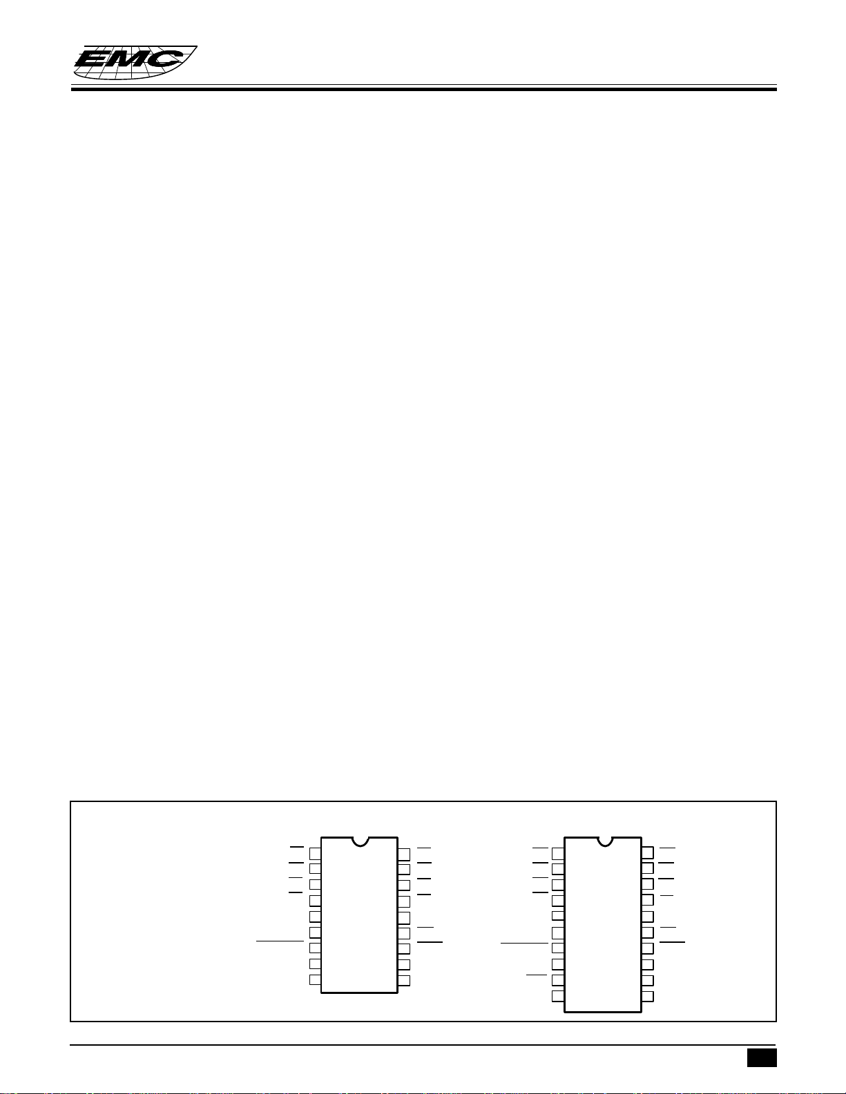
PIN ASSIGNMENTS
EM91810A
C2
1
C3
2
C4
3
C1
4
OSCI
OSCO
XMUTE
V
SDO
5
6
7
SS
8
9
* This specification are subject to be changed without notice.
18
17
16
15
14
13
12
11
10
R3
R2
R1
R4
TONE
PO
HKS
V
DD
KT
C2
C3
C4
C1
OSCI
OSCO
XMUTE
V
HFI
SDO
EM91810B
1
2
3
4
5
6
7
8
SS
9
10
20
19
18
17
16
15
14
13
12
11
R3
R2
R1
R4
TONE
PO
HKS
DD
V
HFO
KT
10.1.1997
1
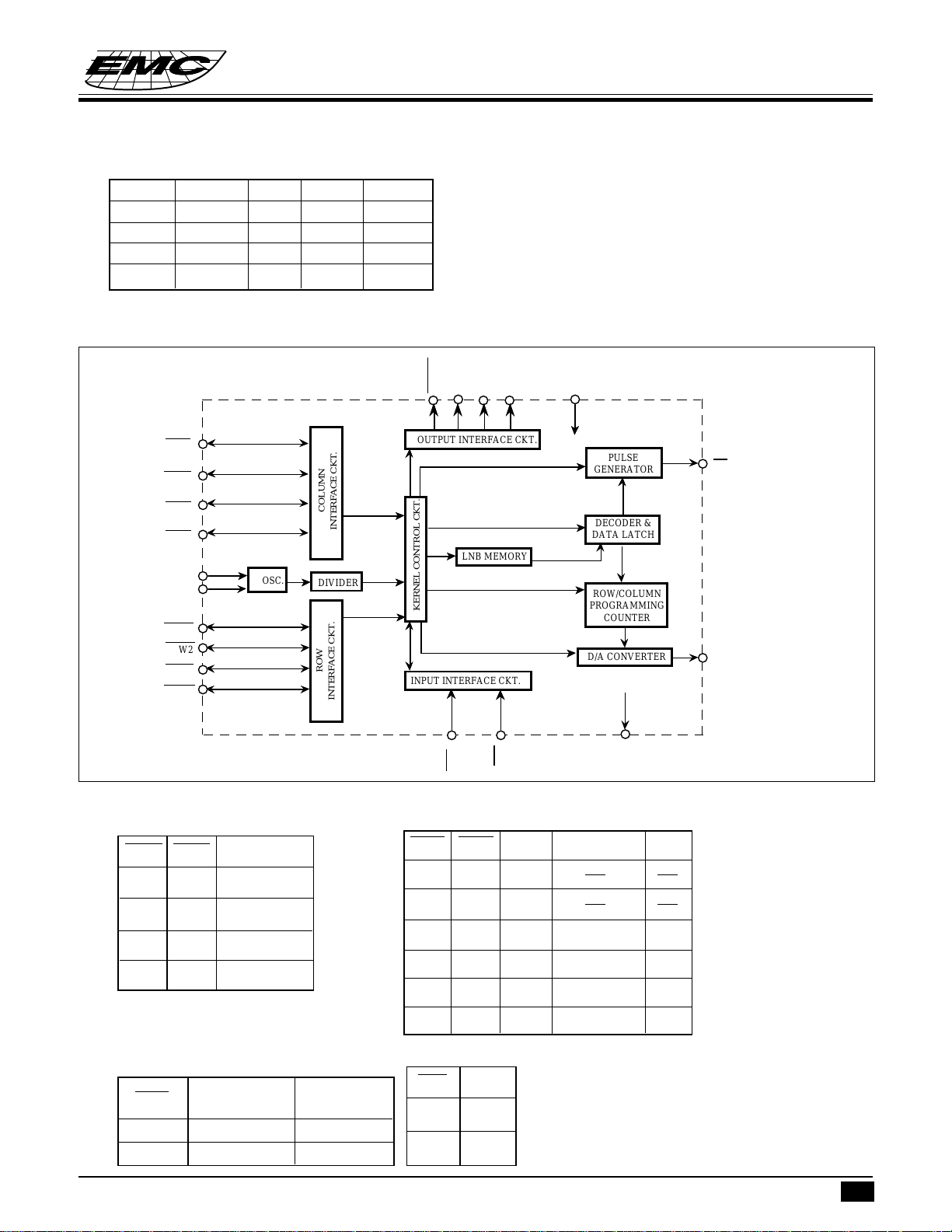
KEYBOARD ASSIGNMENT
EM91810A/B
TONE/PULSE SWITCHABLE DIALER WITH LCD INTERFACE
C1 C2 C3 C4
R1 1 2 3 P→T
R2 456F
R3 789P
R4 *or*/T 0 # RD
FUNCTIONAL BLOCK DIAGRAM
COL1
COL2
COL3
COL4
OSCI
OSCO
ROW1
ROW2
ROW3
ROW4
OSC.
COLUMN
INTERFACE CKT.
DIVIDER
ROW
INTERFACE CKT.
1). P→T : In pulse mode, execute P→T function.
2). F : Flash key.
3). RD : Redial key.
4). P : Pause key.
5). */T : In pulse mode, execte P→T function
KT
SDO
XMUTE
OUTPUT INTERFACE CKT.
LNB MEMORY
KERNEL CONTROL CKT.
INPUT INTERFACE CKT.
HFO
In tone mode, execte "*" key.
DD
V
PULSE
GENERATOR
DECODER &
DATA LATCH
ROW/COLUMN
PROGRAMMING
COUNTER
D/A CONVERTER
PO
TONE
DIALING SIGNAL OPTION :
a]:Flash time:
Row3 Row4
NR
R
R
flash time(ms)
NR
RNR
NR
R
600
300
100
80
c]:Tone function:
Col1
NR
R
Tone Duration
98 ms
83 ms
inter-Tone
Pause
98 ms
83 ms
* This specification are subject to be changed without notice.
b).
Row1 Row2
R NR TONE
R R TONE
NR
NR
UR
UR R PULSE 10PPS 33:66
d]:Key type select
Col2
NR
HKS
NR PULSE
R PULSE
NR PULSE
*or*/T
select
R */T
HFI
MODE PULSE RATE M/B
20PPS 40:60
20PPS 33:66
10PPS 40:60
Note: NR:no resistance.
*
R : A resistance connect to Vss
UR: A resistance connect to V
SS
V
(820KΩ typically)
DD
10.1.1997
2
TONE/PULES SWITCHABLE DIALER WITH LCD INTERFACE
n
PIN DESCRIPTION
Symbol Function
EM91810A/B
C1
C2
C3
C4
R1
R2
R3
R4
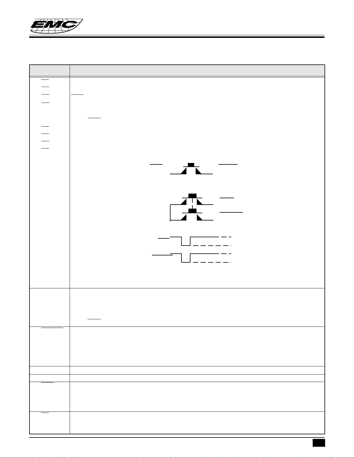
Provides keyboard scanning .
a. Keyboard scanning:
HKS pin is LOW, the column group stays in "HIGH" stays and row group stays in "LOW" state.
The key pad is compatible with the standard dual contact matrix keyboard (as Figure 1b.), the
inexpensive single contact keyboard (as Figure 1a.), and electronic input (as Figure 1c.).
When HKS is “low”, a valid key entry is defined by related Row & Column connection or by
electronic input; (as show in Figure 1c).
Activation of two or more keys will result in no response, except for single key.
To avoid keyboard bouncing error, this chip provides built-in debounce circuit. (The debounce
time = 20 ms.)
Row Column
Figure 1a : Single contact form keyboard configuration
Row
Column
Figure 1b : Dual contact form keyboard configuration
V
Row
Colum
V
V
DD
SS
DD
V
SS
Figure 1c : Electronic signal input keyboard configuration
OSCI
OSCO
Oscillator input & Oscillator output pins.
The 3.579545 MHz oscillator is formed by a built-in inverter inside of this chip and by connecting a
3.579545 MHz crystal or a ceramic resonator across the OSCI and OSCO pins. (built-in feedback
resistor and capacitor)
When HKS is “low”, a valid key-in may turn on this oscillator and generates a 3.579545 MHz clock.
XMUTE
Mute output pins.
NMOS open drain output structure.
The output is in “low” state during dialing sequence (both Pulse and Tone mode) otherwise this pin
is “high-impedance” .
Long (continue) Mute.
V
SS
V
DD
HKS
Negative power supply pin.
Positive power supply pin.
Hook switch input pin.
When the handset is in ON-HOOK state, this pin must be pulled “high” in order to disable the dialing
operation and decrease the power consumption.
When in OFF-HOOK state, the HKS pin must be pulled “low” state for all function operation.
PO
Pulse output signal pin.
NMOS open drain output structure.
The output is “low” during pulse dialing and Flash operation, otherwise this output is “floating”.
* This specification are subject to be changed without notice.
10.1.1997
3
TONE/PULSE SWITCHABLE DIALER WITH LCD INTERFACE
Symbol Function
EM91810A/B
TONE
HFI
HFO
SDO
KT
Dual Tone Multi-frequency output pin.
In TONE mode, when a entry of digit key (include * , # key), this pin will sent out a corresponding
DTMF signal.
The TONE pin provides minimum tone duration (t
key-in. If key-in time is less than t
, DTMF signal will last for tTD , otherwise the tone duration will
TD
),& minimum intertone pause time to support rapid
TD
last as long as the key is pressed.
Handfree input control pin.
Toggle input sturcture, falling edge trigger.
It is used to enable and disable Handfree function.
With waveshaped by a built-in Schmit trigger, the bounce of input can be eliminated by external R,
C debounce circuit.
A built-in pull up resistor is 200K typical.
Handfree output pin.
Inverter output structure (normally "low", active "high").
When a HFI pin is active, Handfree function will be enabled (HFO=1) or disabled (HFO=0).
When the Handfree function is enable (HFO=1), after OFF-HOOK action, it can reset Handfree
function and HFO pin return to "low" state.
Serial data output pin.
NMOS open drain output structure.
When there is a valid entry on keyboard, this pin will output a serial data.
This serial data is designed to drive LCD driver to display dialing number on LCD screen or drive
voice synthesizer to announce dialing number to speaker.
Key tone output pin for key pad input. The key tone duration is the same as the key pressed time.
No matter at Tone mode or pulse mode.
Inverter output structure.
FUNCTION DESCRIPTION
Keyboard Operation
Symbol definitions:
a). ↑ : OFF-HOOK or enable Hand Free function.
b). ↓ : ON-HOOK or disable Hand Free function.
c). : Input level from low to high.
d). : Input level from high to low.
e). D
.....Dn : Digit key; 1,2,3,4,5,6,7,8,9,0,*,# (C1.....Cn is same as D1.....Dn ).
1
f). D
g). D
h). t
i). t
j). t
k). t
l). t
... DPn: Pulse digit ; 1,2,3,4,5,6,7,8,9,0, (CP1... CPn is same as DP1... DPn).
P1
....Dtn: Tone digit ; 1,2,3,4,5,6,7,8,9,0,*, # (Ct1....Ctn is same as Dt1....Dtn).
t1
F
P
PT
FP
RP
: Flash time.
: Pause time.
: Pulse to Tone wait time.
: Pause time for flash.
: Pause time for redial.
m). LNB : Last number redial buffer.
* This specification are subject to be changed without notice.
10.1.1997
4

TONE/PULES SWITCHABLE DIALER WITH LCD INTERFACE
A. Normal Dialing
1. Digit Dialing
Procedure : ↑ D1,D2 . . . . . ., Dn↓
Dial out : Dt1, Dt2 . . . . . . ., Dtn in tone mode
Dial out : Dp1, Dp2 . . . . . ., Dpn in pulse mode
LNB : D1, D2 . . . . . . Dn
2. Dialing with flash key
Procedure : ↑ F,D1,D2 . . . . . ., Dn↓
Dial out : t
Dial out : t
, Dt1,Dt1 . . . . . . ., Dtn in tone mode
F
,Dp1,Dp1 . . . . . . ., Dpn in pulse mode
F
LNB : D1, D2 . . . . . . . Dn
3. Dialing with P→T key
Procedure : ↑ D1, D2 . . . . . .,P→T, . . . . . , Dn↓
Dial out : Dp1, Dp2, . . . . t
, . . . . . , Dtn in pulse mode
PT
LNB : D1, D2 . . . . . ,P→T, . . . . Dn
Note : If key in digit over maximum digit stored in LNB, then RD is inhibited even after on/off hook.
EM91810A/B
B. Mixed dialing
Procedure : ↑ D1, D2 . . . . . .,P→T, D9,D10, . . . . . , Dn↓
Dial out : Dp1, Dp2, . . . . t
, Dt9,Dt10 . . . . . , Dtn
PT
LNB : D1, D2 . . . . . ,P→T, D9,D10 . . . . Dn
C. Redial
LNB : D1, D2 . . . . . Dn
Procedure : ↑ RD ↓
Dial out : Dt1, Dt2, . . . . Dtn in tone mode
Dial out : Dp1, Dp2, . . . . Dpn in pulse mode
Note : If key in digit over maximum digit stored in LNB, then RD is inhibited.
D. Pause Function
Procedure : ↑ D1, D2, . . . .Dn, P, C1 . . . . .Cn↓
Dial out : Dt1, Dt2, . . . . Dtn , tp, Ct1 . . . . . . . . . Ctn in tone mode
Dial out : Dp1, Dp2, . . . . Dpn,tp, Cp1 . . . . . . . . .Cpn in pulse mode
LNB : D1, D2 . . . . . Dn, P, C1, C2 . . . . . . . . . .Cn
E. Flash Function
1. Reset
Procedure : ↑ D1, D2, . . . .Dn, F, C1 . . . . .Cn ↓
Dial out : Dt1, Dt2, . . . . Dtn , t
Dial out : Dp1, Dp2, . . . . Dpn, t
,Ct1 . . . . . . . . . Ctn in tone mode
F
,Cp1 . . . . . . . . .Cpn in pulse mode
F
LNB : C1, C2 . . . . . Cn
* This specification are subject to be changed without notice.
10.1.1997
5
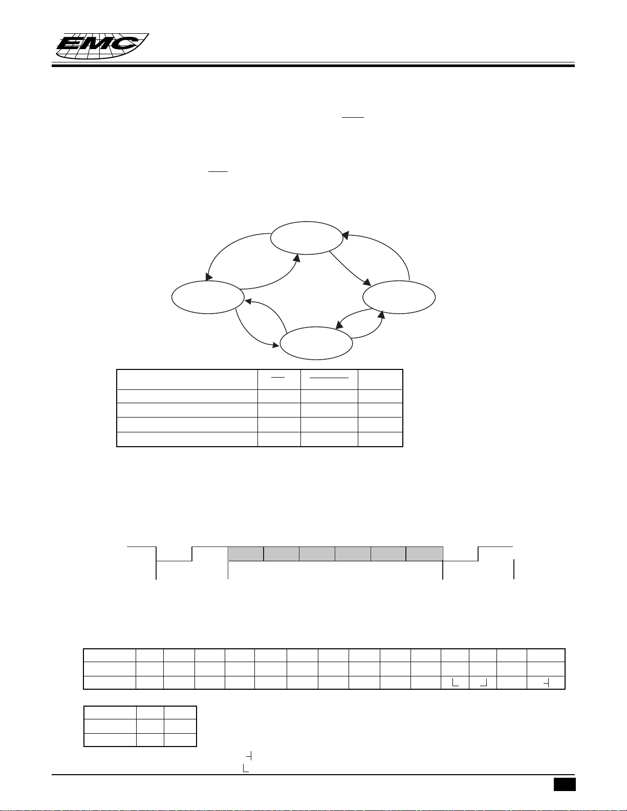
Handfree function operation:
A). To execute Handfree function : When HFO = "low", HFI pin is active , the Handfree function will be
enabled (HFO="HIGH").
B). Reset Handfree function:
a. OFF-HOOK action.
b. When HFO="high", a HFI pin is active again , the Handfree function will be reset (HFO="LOW").
Operating flow chart of Handfree
EM91810A/B
TONE/PULSE SWITCHABLE DIALER WITH LCD INTERFACE
HF
ON HKS
HF LINE
STATE NO. PO XMUTE HFO
(0) INITIAL STATE F F 0
(1) ON HKS HF LINE F F 1
(2) OFF HKS LINE F F 0
(3) OFF HKS HF LINE F F 1
* F : Floating (Hi-impedance)
SDO (Serial Data Output) function
The SDO is serial data output which format is the same with UART protocol. SDO function is designed to drive
LCD driver and voice synthesizer to display dialing number on LCD screen and announce it to speaker. The SDO
signal consists of two start bits, six data bits and two stop bits.
(1)
OFF
ON
ON HKS
INITIAL
HF
OFF HKS
HF LINE
(0)
(3)
HF
OFF
HF
OFF HKS
ON
(2)
* Note :
ON : ON HKS
OFF : OFF HKS
HF : Depress HF key
0 1 Bit0 Bit1 Bit2 Bit3 Bit4 Bit5 0 1
Start bit Data bits
LSB
The frequency of every bit is 256Hz (about 3.9 ms)
There are two categories of dialing data, and representation of serial data is as the following:
(b5,b4=0,0) Digit key
Key 1234 56 78 9 0*#PP-T
b3b2b1b0 0001 0010 0011 0100 0101 0110 0111 1000 1001 1010 1011 1100 1101 1110
Display 1 2 3 4 5 6 7 8 9 0 P
(b5,b4=1,0) Function key
Key HF F
b3b2b1b0 1010 1111
Display F
Note : */T key at pulse mode display " "
at tone mode display " "
* This specification are subject to be changed without notice.
MSB
Stop bit
10.1.1997
6
 Loading...