ELAN EM78P156E Datasheet

EM78P156E
I. GENERAL DESCRIPTION
EM78P156E is an 8-bit microprocessor with low-power and high-speed CMOS technology. There is a 1K*13bit Electrical One Time Programmable Read Only Memory (OTP-ROM) within it. It provides a PROTECTION
bit to prevent a user’s code from intruding as well as 7 OPTION bits to match the user’s requirements.
Because of the OTP-ROM, the EM78P156E offers users a convenient way to develop and verify their programs.
Moreover, a user’s developed code can be programmed easily by an EMC writer.
II. FEATURES
• Operating voltage range: 2.2V~5.5V
• Available in temperature range: 0°C~70°C
• Operating frequency range: DC ~ 36MHz
• Low power consumption:
* less than 1.6 mA at 5V/4MHz
* typical of 15 µA at 3V/32KHz
* typical of 1 µA during the sleep mode
• 1Kx13 bits on chip ROM
• One security register to prevent the code in the OTP memory from intruding
• One configuration register to match the user’s requirements
• 48x8 bits on chip registers (SRAM)
• 2 bi-directional I/O ports
• 5 level stacks for subroutine nesting
• 8-bit real time clock/counter (TCC) with selective signal sources, trigger edges, and overflow interrupt
• Two clocks per instruction cycle
• Power-down mode (SLEEP mode)
• Three available interruptions
* TCC overflow interrupt
* Input-port status changed interrupt (wake up from the sleep mode)
* External interrupt
• Programmable free running watchdog timer
• 8 pull-high pins
• 7 pull-down pins
• 8 open-drain pins
• Two R-option pins
• Package type: SOP, SOIC and DIP
• 99.9% single instruction cycle commands
* This specification is subject to be changed without notice. 8.11.1999
B3-1
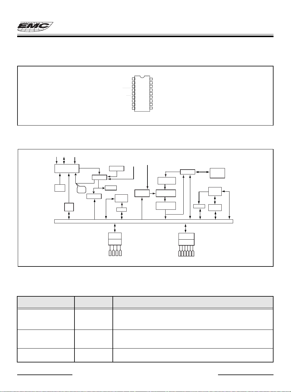
III. PIN ASSIGNMENTS
EM78P156E
EM78P156E
P52
1
P53
2
TCC
3
RESET
4
SS
V
5
P60,INT
6
P61
7
P62
8
P63
9
DIP
SOP
SOIC
Fig. 1 Pin assignments
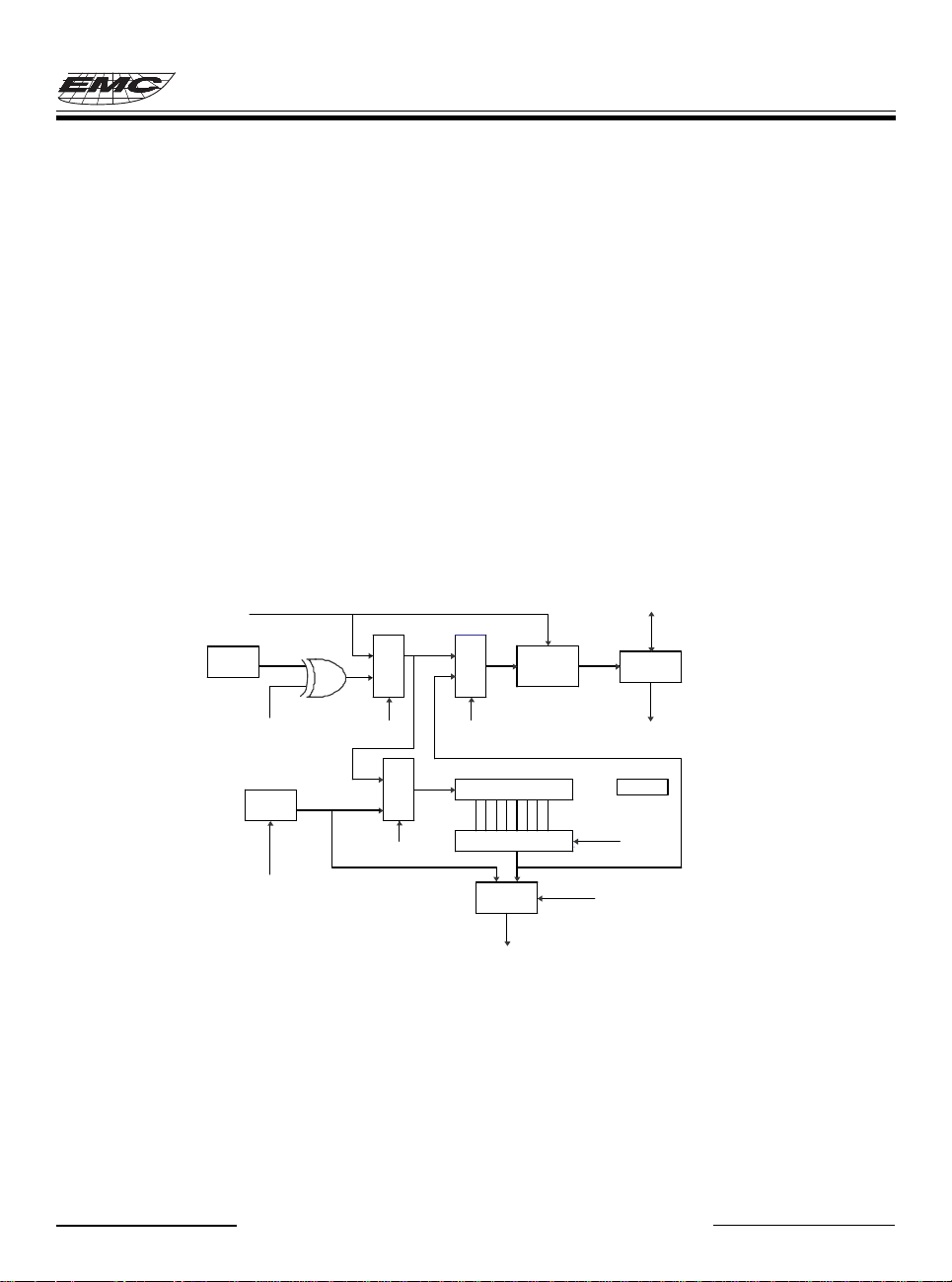
IV. FUNCTIONAL BLOCK DIAGRAM
OSCI OSCO /RESET
Oscillator/Timing
Control
Internal C
External R
oscillator
Sleep
& Wake
Control
WDT
Time-out
WDT Timer
Prescaler
IOCA
R1(TCC)
IOC5
TCC
Interrupt
RAM
Controller
R4
DATA & CONTROL BUS
R5
/INT
P51
18
P50
17
OSCI
16
OSCO
15
V
DD
14
P67
13
P66
12
P65
11
P64
10
R2
Stack
ROM
Instruction
register
Instruction
Decoder
ALU
R3
ACC
IOC6
R6
P
P
P
P
5
5
5
5
0
2
3
1
P
P
P
P
P
P
P
P
6
6
6
6
6
6
6
6
0
2
3
1
4
6
7
5
Fig. 2 Functional block diagram
V. PIN DESCRIPTION
Table 1 Pin description-EM78P156E
Symbol I/O Function
OSCI I *XTAL type : Crystal input terminal or external clock input pin.
*ERC type: RC oscillator input pin.
*IRC type: 50K ohm pulled high for 4MHz.
OSCO I/O * XTAL type: Output terminal for crystal oscillator or external clock input pin.
*RC type: Instruction clock ouput.
*External clock signal input.
TCC I * Real time clock/counter with Schmitt trigger input pin, must be tied to V
or VSS if not in use.
* This specification is subject to be changed without notice. 8.11.1999
B3-2
DD

EM78P156E
Symbol I/O Function
/RESET I * Input pin with Schmitt trigger. If this pin remains at logic low, the controller
will keep in reset condition.
P50~P53 I/O *P50~P53 are bi-directional I/O pins. P50 and P51 can also be defined as the
R-option pins. P50~P52 can be pulled down by software .
P60~P67 I/O *P60~P67 are bi-directional I/O pins. These can be pull-high or can be open-
drain by software programming. In addition, P60~P63 can be pull-down
also by software.
/INT I * External interrupt pin triggered by falling edge.
V
DD
V
SS
VI. FUNCTION DESCRIPTION
VI.1 Operational Registers
1. R0 (Indirect Addressing Register)
• R0 is not a physically implemented register. Its major function is to be an indirect addressing pointer. Any instruction
using R0 as a pointer actually accesses data pointed by the RAM Select Register (R4).
- * Power supply.
- * Ground.
2. R1 (Time Clock /Counter)
• Increased by an external signal edge which is defined by TE bit (CONT-4) through the TCC pin,
or by the instruction cycle clock.
• Writable and readable as any other registers.
3. R2 (Program Counter) & Stack
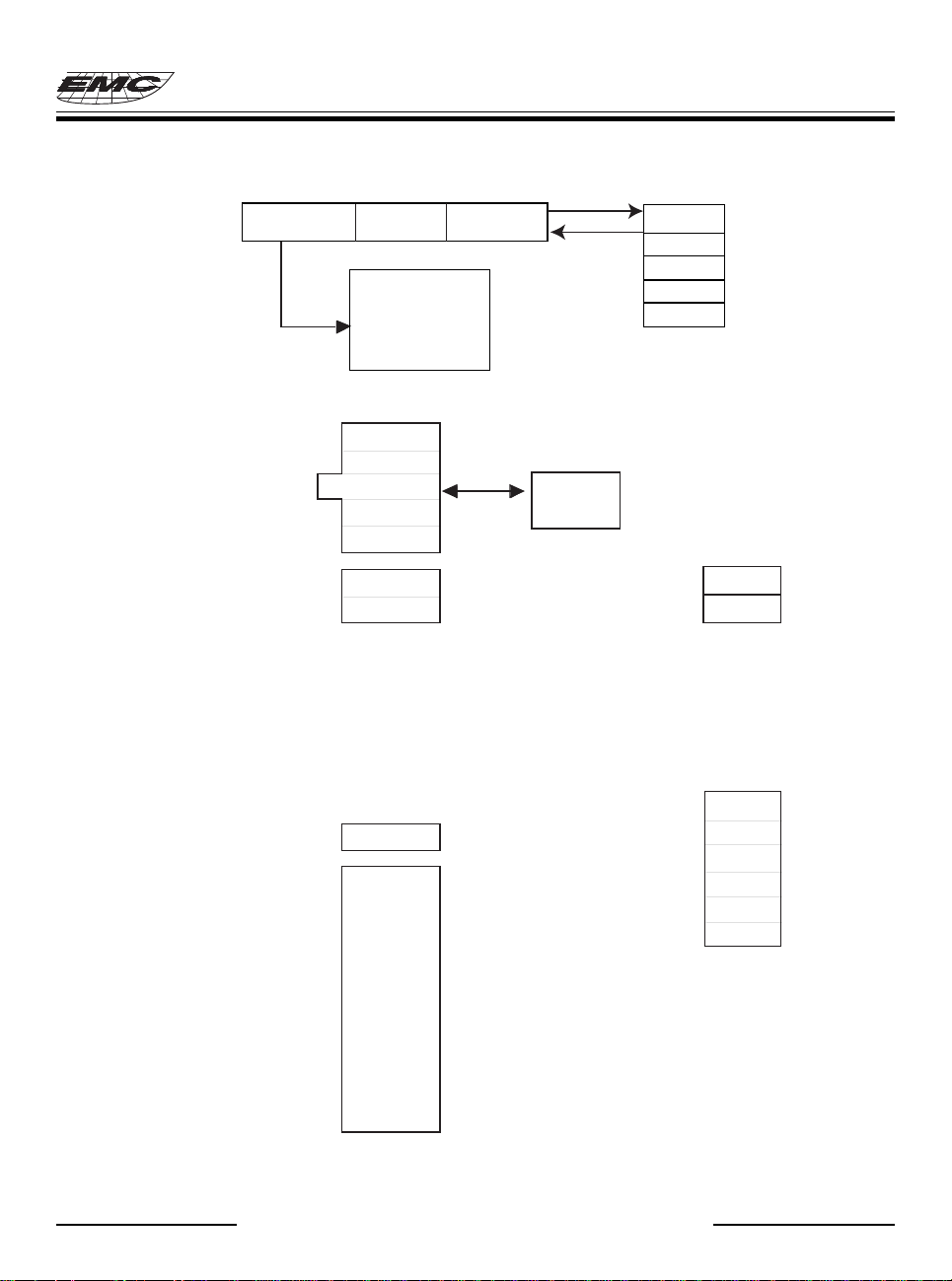
• R2 and hardware stacks are 10~12-bit wide. The structure is depicted in Fig. 3.
• Generating 1024x13 bits on-chip OTP ROM addresses to the relative programming instruction codes. One program
page is 1024 words long.
• The contents of R2 are set all “0”s upon a RESET condition.
• “JMP” instruction allows the direct loading of the lower 10 program counter bits. Thus, “JMP” allows PC to go to
any location within a page.
• “CALL” instruction loads the lower 10 bits of the PC, and then PC+1 is pushed into the stack. Thus, the subroutine
entry address can locate anywhere within a page.
“ RET” (“RETL K”, “RETI”) instruction loads the program counter with the contents of the top-level stack.
“ADD R2,A” allows a relative address to be added to the current PC, and the ninth and tenth bits of the PC are cleared.
• “MOV R2,A” allows to load an address from the “A” register to the lower 8 bits of the PC, and the ninth and tenth
bits of the PC are cleared.
• Any instruction which would change the contents of R2 (e.g. “ADD R2,A”, “MOV R2,A”, “BC R2,6”,......) will
cause the ninth and tenth bits (A8~A9) of the PC to be cleared. Thus, the computed jump is limited to the first
256 locations of a page.
• All instructions are single instruction cycle (fclk/2) except the instructions which would change the contents of R2
need one more instruction cycle.
* This specification is subject to be changed without notice. 8.11.1999
B3-3
CALL
IOC5
IOC6
IOCA
IOCB
IOCC
IOCD
IOCE
IOCF
Stack
(5 levels)
R0
R1(TCC)
R2(PC)
R3(Status)
R4(RSR)
00
01
02
03
04
R5(Port5)
R6(Port6)
RF
R10
:
:
48x8
Common
Register
R3F
05
06
07
08
09
0A
0B
0C
0D
0E
0F
10
:
:
3F
A11 A10 A9 A8 A7 ~ A0 Stack 1
PC
RET
000
00
PAGE 0
3FF
Fig. 3 Program counter organization
RETI
RETL
EM78P156E
Stack 2
Stack 3
Stack 4
Stack 5
Fig. 4 Data memory configuration
* This specification is subject to be changed without notice. 8.11.1999
B3-4

EM78P156E
4. R3 (Status Register)
7 6 543210
GP2 GP1 GP0 T P Z DC C
• Bit 0 (C) Carry flag
• Bit 1 (DC) Auxiliary carry flag
• Bit 2 (Z) Zero flag. Set to "1" if the result of an arithmetic or logic operation is zero.
• Bit 3 (P) Power-down bit. Set to 1 during power-on or by a “WDTC” command and reset to 0 by a
“SLEP” command.
• Bit 4 (T) Time-out bit. Set to 1 by the “SLEP” and “WDTC” commands, or during power-up and reset
to 0 by WDT time-out.
• Bit 5~7 (GP0~2) General-purpose read/write bits.
5. R4 (RAM Select Register)
• Bits 0 ~ 5 are used to select registers (address: 00~06, 0F~3F) in the indirect addressing mode.
• Bits 6 ~ 7 are general-purpose read/write bits.
• See the configuration of the data memory in Fig.4.
6. R5 ~ R6 (Port 5 ~ Port 6)
• R5 and R6 are I/O registers.
• Only the lower 4 bits of R5 are available.
7. RF (Interrupt Status Register)
76 5 4 32 10
- - - - - EXIF ICIF TCIF
• "1" means interrupt request, and "0" means non-interrupt occurence.
• Bit 0 (TCIF) TCC overflowing interrupt flag. Set when TCC timer overflows, reset by software.
• Bit 1 (ICIF) Port 6 input status changed interrupt flag. Set when Port 6 input changes, reset by software.
• Bit 2 (EXIF) External interrupt flag. Set by falling edge on /INT pin, reset by software.
• Bits 3 ~ 7 Not used.
• RF can be cleared by instruction but can not be set.
• IOCF is the interrupt mask register.
• Note that the result of reading RF is the "logic AND" of RF and IOCF.
8. R10 ~ R3F
• All of these are the 8-bit general-purpose registers.
VI.2 Special Purpose Registers
1. A (Accumulator)
* This specification is subject to be changed without notice. 8.11.1999
B3-5
• Internal data transfer, or instruction operand holding
• It can not be addressed.
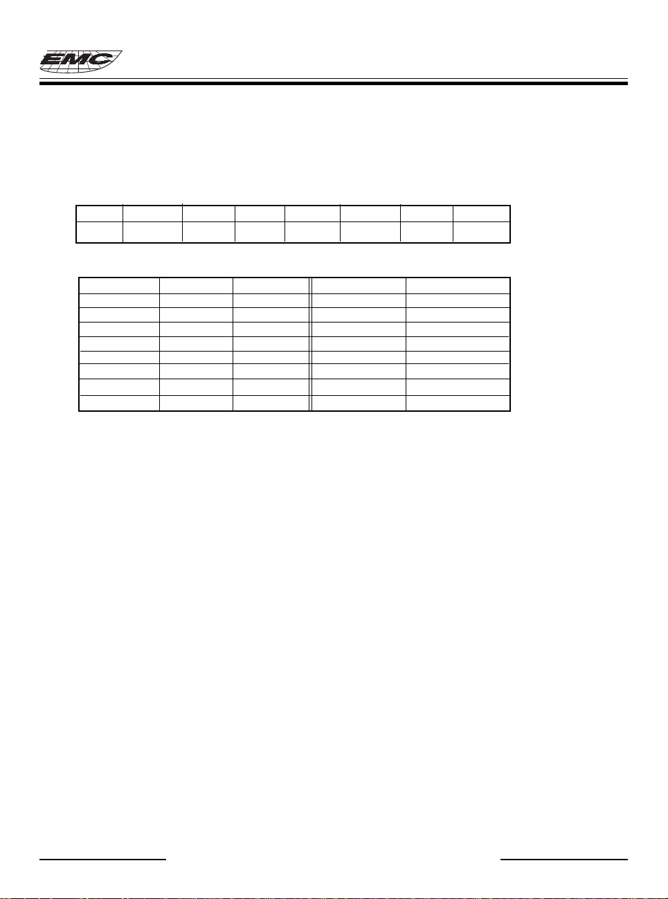
2. CONT (Control Register)
76 543 21 0
- /INT TS TE PAB PSR2 PSR1 PSR0
Bit 0 (PSR0)~Bit 2 (PSR2) TCC/WDT prescaler bits.
PSR2 PSR1 PSR0 TCC Rate WDT Rate
0 0 0 1:2 1:1
0 0 1 1:4 1:2
0 1 0 1:8 1:4
0 1 1 1:16 1:8
1 0 0 1:32 1:16
1 0 1 1:64 1:32
1 1 0 1:128 1:64
1 1 1 1:256 1:128
Bit 3 (PAB) Prescaler assignment bit.
0: TCC
1: WDT
Bit 4 (TE) TCC signal edge
0: increment if the transition from high to low takes place on TCC pin
1: increment if the transition from high to low takes place on TCC pin
Bit 5 (TS) TCC signal source
0: internal instruction cycle clock
1: transition on TCC pin
Bit 6 (INT) Interrupt enable flag
0: masked by DISI or hardware interrupt
1: enabled by ENI/RETI instruction
• CONT register is both readable and writable.
EM78P156E
3. IOC5 ~ IOC6 (I/O Port Control Register)
• “1” puts the relative I/O pin into high impedance, while “0” defines the relative I/O pin as output.
• Only the lower 4 bits of IOC5 are able to be defined.
• IOC5 and IOC6 registers are both readable and writable.
4. IOCA (Prescaler Counter Register)
• IOCA register is readable.
• The value of IOCA is equal to the contents of Prescaler counter.
• Down counter.
* This specification is subject to be changed without notice. 8.11.1999
B3-6
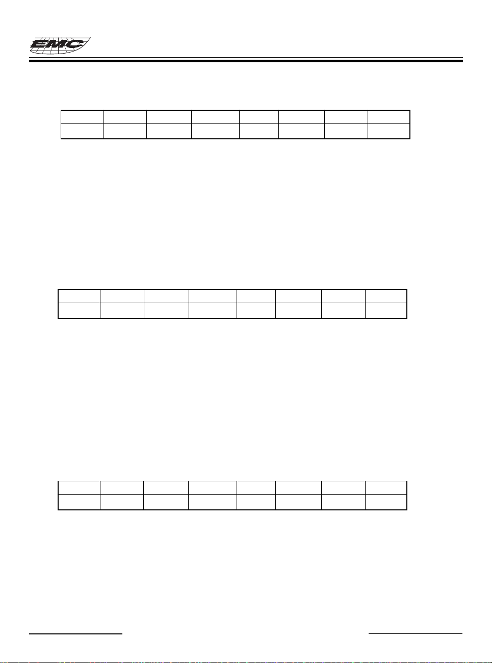
5. IOCB (Pull-down Control Register)
76543210
/PD7 /PD6 /PD5 /PD4 - /PD2 /PD1 /PD0
Bit 0 (/PD0) Control bit used to enable the pull-down of P50 pin.
0: Enable internal pull-down
1: Disable internal pull-down
Bit 1 (/PD1) Control bit used to enable the pull-down of P51 pin.
Bit 2 (/PD2) Control bit used to enable the pull-down of P52 pin.
Bit 3 Not used.
Bit 4 (/PD4) Control bit used to enable the pull-down of P60 pin.
Bit 5 (/PD5) Control bit used to enable the pull-down of P61 pin.
Bit 6 (/PD6) Control bit used to enable the pull-down of P62 pin.
Bit 7 (/PD7) Control bit used to enable the pull-down of P63 pin.
• IOCB register is both readable and writable.
6. IOCC (Open-drain Control Register)
76543210
OD7 OD6 OD5 OD4 OD3 OD2 OD1 OD0
Bit 0 (OD0) Control bit used to enable the open-drain of P60 pin.
0: Disable open-drain output
1: Enable open-drain output
Bit 1 (OD1) Control bit used to enable the open-drain of P61 pin.
Bit 2 (OD2) Control bit used to enable the open-drain of P62 pin.
Bit 3 (OD3) Control bit used to enable the open-drain of P63 pin.
Bit 4 (OD4) Control bit used to enable the open-drain of P64 pin.
Bit 5 (OD5) Control bit used to enable the open-drain of P65 pin.
Bit 6 (OD6) Control bit used to enable the open-drain of P66 pin.
Bit 7 (OD7) Control bit used to enable the open-drain of P67 pin.
• IOCC register is both readable and writable.
EM78P156E
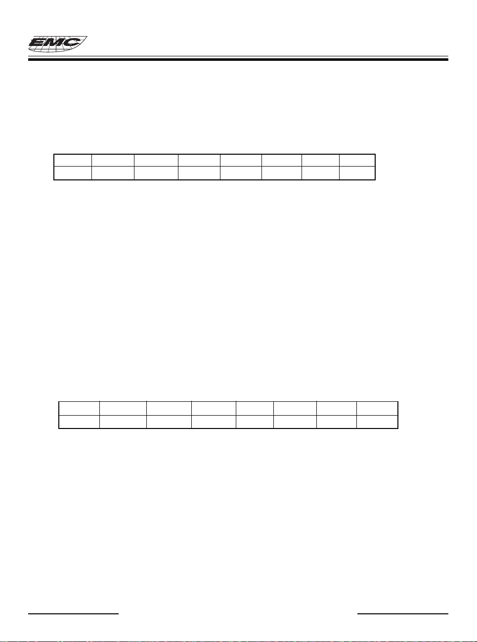
7. IOCD (Pull-high Control Register)
765 43210
/PH7 /PH6 /PH5 /PH4 /PH3 /PH2 /PH1 /PH0
Bit 0 (/PH0) Control bit used to enable the pull-high of P60 pin.
0: Enable internal pull-high
1: Disable internal pull-high
Bit 1 (/PH1) Control bit used to enable the pull-high of P61 pin.
Bit 2 (/PH2) Control bit used to enable the pull-high of P62 pin.
Bit 3 (/PH3) Control bit used to enable the pull-high of P63 pin.
Bit 4 (/PH4) Control bit used to enable the pull-high of P64 pin.
Bit 5 (/PH5) Control bit used to enable the pull-high of P65 pin.
* This specification is subject to be changed without notice. 8.11.1999
B3-7
EM78P156E
Bit 6 (/PH6) Control bit used to enable the pull-high of P66 pin.
Bit 7 (/PH7) Control bit used to enable the pull-high of P67 pin.
• IOCD register is readable and writable.
8. IOCE (WDT Control Register)
76543210
WDTE EIS - ROC - - - -
Bit 7 (WDTE) Control bit used to enable Watchdog Timer.
0: Disable WDT.
1: Enable WDT.
• WDTE is both readable and writable.
Bit 6 (EIS) Control bit used to define the function of P60 (/INT) pin.
0: P60, bi-directional I/O pin.
1: /INT, external interrupt pin. In this case, the I/O control bit of P60 (bit 0 of IOC6) must be set to “1”.
• When EIS is “0”, the path of /INT is masked. When EIS is “1”, the status of /INT pin can also be read by
way of reading Port 6 (R6). Refer to Fig.7(a).
• EIS is both readable and writable.
Bit 4 (ROC) ROC is used for the R-option.
Setting the ROC to “1” will enable the status of R-option pins (P50~P51) to be read by the controller. Clearing
the ROC will disable the R-option function. If the R-option function is selected, the user must connect the P51
pin or/and P50 pin to VSS by a 430KΩ external resistor (Rex). If the Rex is connected/disconnected, the status
of P50 (P51) will be read as “0”/”1". Refer to Fig.8.
• ROC is readable and writable.
Bits 0~3, 5 Not used.
9. IOCF (Interrupt Mask Register)
76543210
- - - - - EXIE ICIE TCIE
Bit 0 (TCIE) TCIF interrupt enable bit.
0: disable TCIF interrupt
1: enable TCIF interrupt
Bit 1 (ICIE) ICIF interrupt enable bit.
0: disable ICIF interrupt
1: enable ICIF interrupt
Bit 2 (EXIE) EXIF interrupt enable bit.
0: disable EXIF interrupt
1: enable EXIF interrupt
Bits 3~7 Not used.
• Individual interrupt is enabled by setting its associated control bit in the IOCF to “1”.
• Global interrupt is enabled by the ENI instruction and is disabled by the DISI instruction. Refer to Fig.10.
• IOCF register is both readable and writable.
* This specification is subject to be changed without notice. 8.11.1999
B3-8
EM78P156E
VI.3 TCC/WDT & Prescaler
There is an 8-bit counter available as prescaler for the TCC or WDT. The prescaler is available for the TCC only
or the WDT only at the same time and the PAB bit of the CONT register is used to determine the prescaler assigment.
The PSR0~PSR2 bits determine the ratio. The prescaler will be cleared by the instructions which write to TCC each time,
when assigned to TCC mode. The WDT and prescaler, when assigned to WDT mode, will be cleared by the “WDTC”
and “SLEP” instructions. Fig.5 depicts the circuit diagram of TCC/WDT.
• R1 (TCC) is an 8-bit timer/counter. The clock source of TCC can be internal clock or external clock input (edge
selectable from TCC pin). If TCC signal source is from internal clock, TCC will increase by 1 in every instruction
cycle (without prescaler). Refer to Fig.5, CLK=Fosc/2 or CLK=Fosc/4 is depended on the CODE option bit CLKS.
CLK=Fosc/2 if CLKS bit is “0”, and CLK=Fosc/4 if CLKS bit is “1”. If TCC signal source is from external clock
input, TCC will increase by 1 on every falling edge or rising edge of TCC pin.
• The watchdog timer is a free running on-chip RC oscillator. The WDT will keep running even the oscillator driver
has been turned off (i.e. in sleep mode). During the normal operation or the sleep mode, a WDT time-out (if enabled)
will cause the device to reset. The WDT can be enabled or disabled at any time during the normal mode by software
programming. Refer to WDTE bit of IOCE register. With no presacler, the WDT time-out period is approximately
18 ms.
CLK(Fosc/2 or Fosc/4)
TCC
Pin
Data Bus
0
1
1
M
U
X
M
U
X
0
SYNC
2 cycles
TCC(R1)
TE
WDT
WDTE
(in IOCE)
TS PAB
0
M
U
1
X
PAB
8-bit Counter
8-to-1 MUX
1
0
MUX
WDT time-out
TCC overflow interrupt
IOCA
PSR0 ~PSR2
PAB
Fig. 5 Block diagram of TCC and WDT
VI.4 I/O Ports
The I/O registers, both Port 5 and Port 6, are bi-directional tri-state I/O ports. Port 6 can be pulled high internally
by software. In addition, Port 6 can also have open-drain output by software. There is an input status changed interrupt
(or wake-up) function on Port 6. P50 ~ P52 and P60 ~ P63 pins can be pulled down by software. Each I/O pin can be
defined as “input” or “output” pin by the I/O control registers (IOC5 ~ IOC6). P50~P51 are the R-option pins enabled
by setting the ROC bit in the IOCE register to 1. While the R-option function is used, P50~P51 are recommended to be
used as output pins. During the period of R-option being enabled, P50~P51 must be programmed as input pins. In the
R-option mode, the current consuming by the Rex should be taken into the consideration, if the low power consumption
is concerned.
* This specification is subject to be changed without notice. 8.11.1999
B3-9
 Loading...