

ELAN EM78P153E User Manual

EM78P153E
OTP ROM
1. GENERAL DESCRIPTION
EM78P153E is an 8-bit microprocessor with low-power and high-speed CMOS technology. It is equipped
with a 512*13-bits Electrical One Time Programmable Read Only Memory (OTP-ROM). It provides a
PROTECTION bit to prevent intrusion of user’s code in the OTP memory as well as 15 OPTION bits to
match user’s requirements.
With its OTP-ROM feature, the EM78P153E offers users a convenient way of developing and verifying
their programs. Moreover, user developed code can be easily programmed with the EMC writer.
This specification is subject to change without prior notice. 2002/03/01 1

2. FEATURES
• 14-lead packages : EM78P153E
• Operating voltage range : 2.3V~5.5V
• Available in temperature range: 0°C~70°C
• Operating frequency rang (base on 2 clocks ):
* Crystal mode: DC~20MHz at 5V, DC~8MHz at 3V, DC~4MHz at 2.3V.
* ERC mode: DC~4MHz at 5V, DC~4MHz at 3V, DC~4MHz at 2.3V.
• Low power consumption:
* less then 1.5mA at 5V/4MHz
EM78P153E
OTP ROM
* typical of 15 µA, at 3V/32KHz
* typical of 1 µA, during the sleep mode
• 512 × 13 bits on chip ROM
• Three built-in calibrated IRC oscillators
• Programmable prescaler of oscillator set-up time
• On-board bit by bit programming
• One security register to prevent the code in the OTP memory from intruding
• One configuration register to match the user’s requirements
• 32× 8 bits on chip registers (SRAM, general purpose register)
• 2 bi-directional I/O ports
• 5 level stacks for subroutine nesting
• 8-bit real time clock/counter (TCC) with selective signal sources, trigger edges, and overflow interrupt
• Power down mode (SLEEP mode)
• Three available interruptions
* TCC overflow interrupt
* Input-port status changed interrupt (wake up from the sleep mode)
* External interrupt
• Programmable free running watchdog timer
• 7 programmable pull-high I/O pins
• 7 programmable open-drain I/O pins
• 6 programmable pull-down I/O pins
• Two clocks per instruction cycle
• 99.9% single instruction cycle commands
This specification is subject to change without prior notice. 2002/03/01 2

EM78P153E
• Package types:
* 14 pin DIP 300mil: EM78P153EP
* 14 pin SOP 150mil: EM78P153EN
• The transient point of system frequency between HXT and LXT is around 400KHz.
OTP ROM
This specification is subject to change without prior notice. 2002/03/01 3
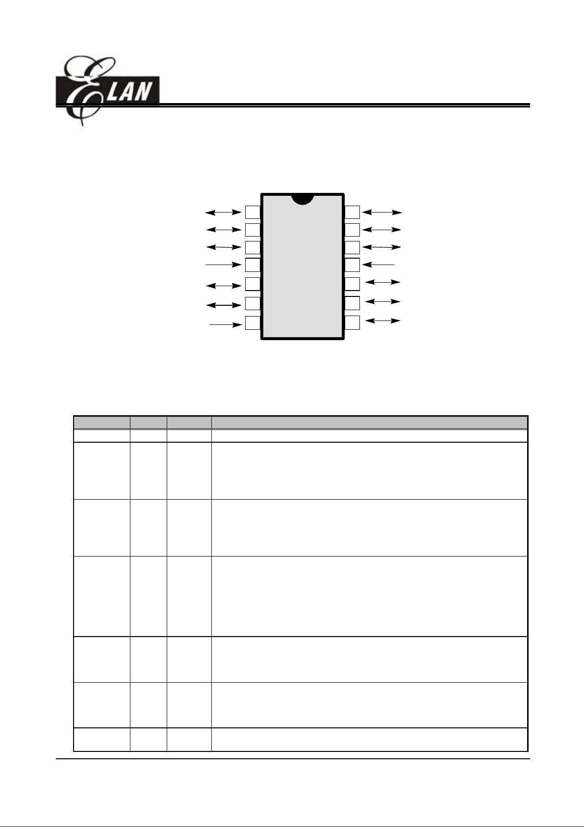
3. PIN ASSIGNMENTS
EM78P153E
P50
P67
P66
Vdd
P65/OSCI
P63//RST
P64/OSCO
EM78P153E
OTP ROM
1
2
3
4
5
6
7
14
13
12
11
1 0
9
8
P51
P52
P53
Vss
P60//INT
P61
P62/TCC
Fig. 1 Pin Assignment
Table 1 Pin Description
Symbol Pin No. Type Function
Vdd 4 - Power supply.
* General purpose I/O pin.
* External clock signal input.
P65/OSCI 5 I/O
* Input pin of XT oscillator.
* Pull_high/open-drain
* Wake up from sleep mode when the status of the pin changes.
* General purpose I/O pin.
* External clock signal input.
P64/OSCO 6 I/O
* Input pin of XT oscillator.
* Pull_high/open-drain
* Wake up from sleep mode when the status of the pin changes.
* If set as /RESET and remain at logic low, the device will be under reset.
* If P63 is set and kept at logic “high,” the oscillator will oscillate.
* If kept at logic low, it cannot oscillate.
P63/RESET 7 I
* Wake up from sleep mode when the status of the pin changes.
* Voltage on /RESET must not exceed Vdd during the normal mode.
* Pull_high is on if defined as /RESET.
* P63 is input pin only
* General purpose I/O pin.
P62/TCC 8 I/O
* Pull_high/open_drain/pull_down.
* Wake up from sleep mode when the status of the pin changes.
* External Timer/Counter input.
* General purpose I/O pin.
P61 9 I/O
P60//INT 10 I/O
This specification is subject to change without prior notice. 2002/03/01 4
* Pull_high/open_drain/pull_down.
* Wake up from sleep mode when the status of the pin changes.
* Schmitt Trigger input during programming mode
* General purpose I/O pin.
* Pull_high/open_drain/pull_down.

* Wake up from sleep mode when the status of the pin changes.
* Schmitt Trigger input during the programming mode.
* External interrupt pin triggered by falling edge.
* General purpose I/O pin.
P66, P67 2, 3 I/O
P50~P52 1,14,13 I/O
P53 12 I/O * General purpose I/O pin.
VSS 11 - * Ground.
* Pull-high/open-drain.
* Wake up from sleep mode when the status of the pin changes.
* General purpose I/O pin.
* Pull-down
EM78P153E
OTP ROM
This specification is subject to change without prior notice. 2002/03/01 5
4. FUNCTION DESCRIPTION
OSCO
OSCI
Oscillator/Timing
Control
/RESET
WDT timer
Prescaler
TCC /INT
ROM
R2
EM78P153E
OTP ROM
Stack
Built-in
OSC
RAM
R3
R1(TCC)
Interrupt
Controller
DATA & CONTROL BUS
IOC6
R6
Fig. 2 Function Block Diagram
4.1 Operational Registers
1. R0 (Indirect Addressing Register)
R0 is not a physically implemented register. Its major function is to be an indirect addressing pointer.
Any instruction using R0 as a pointer, actually accesses data pointed by the RAM Select Register
I/O
PORT 6
Instruction
Register
Instruction
Decoder
P60
P61
P62/TCC
P63/REST
P64/OSCO
P65/OSCI
P66
P67
ALU
R3
ACC
(R4).
2. R1 (Time Clock /Counter)
• Increased by an external signal edge, which is defined by TE bit (CONT-4) through the TCC pin, or
by the instruction cycle clock.
• Writable and readable as any other registers.
• Defined by resetting PAB(CONT-3).
• The prescaler is assigned to TCC if the PAB bit (CONT-3) is reset.
• The contents of the prescaler counter is cleared only when a value is written to TCC register.
This specification is subject to change without prior notice. 2002/03/01 6
EM78P153E
OTP ROM
3. R2 (Program Counter) & Stack
• Depending on the device type, R2 and hardware stack are 9-bit wide. The structure is depicted in
Fig.3.
• 512×13 bits on-chip OTP ROM addresses to the relative programming instruction codes. One
program page is 512 words long.
• R2 is set as all "0"s when under RESET condition.
• "JMP" instruction allows direct loading of the lower 9 program counter bits. Thus, "JMP" allows PC to
go to any location within a page.
• "CALL" instruction loads the lower 9 bits of the PC, and then PC+1 is pushed into the stack. Thus,
the subroutine entry address can be located anywhere within a page.
• "RET" ("RETL k", "RETI") instruction loads the program counter with the contents of the top-level
stack.
• "ADD R2,A" allows the contents of ‘A’ to be added to the current PC, and the ninth of the PC are
cleared.
• "MOV R2,A" allows to load an address from the "A" register to the lower 8 bits of the PC, and the
ninth bits of the PC are cleared.
• Any instruction that is written to R2 (e.g. "ADD R2,A", "MOV R2,A", "BC R2,6",⋅⋅⋅⋅⋅) will cause the
ninth bits (A8) of the PC to be cleared. Thus, the computed jump is limited to the first 256 locations
of a page.
• All instructions are single instruction cycle (fclk/2 or fclk/4), except for the instruction that would
change the contents of R2. This instruction will need one more instruction cycle.
PC 0 0
00
A8
000
1FF
A7 ~ A0
Page 0
CALL
RET
RETL
RETL K
Stack 1
Stack 2
Stack 3
Stack 4
Stack 5
Fig. 3 Program Counter Organization
This specification is subject to change without prior notice. 2002/03/01 7
EM78P153E
OTP ROM
00
01
02
03
04
05
06
0B
0C
0D
0E
0F
R0
R1(TCC)
R2(PC)
R3(Status)
R4(RSR)
R5(Port5)
R6(Port6)
RF
CONT
Stack
(5 levels)
IOC5
IOC6
IOCB
IOCC
IOCD
IOCE
IOCF
R10
.
.
.
.
General
Registers
R2F
Fig. 4 Data Memory Configuration
This specification is subject to change without prior notice. 2002/03/01 8

EM78P153E
OTP ROM
4. R3 (Status Register)
7 6 5 4 3 2 1 0
RST GP1 GP0 T P Z DC C
• Bit 0 (C) Carry flag
• Bit 1 (DC) Auxiliary carry flag
• Bit 2 (Z) Zero flag.
Set to "1" if the result of an arithmetic or logic operation is zero.
• Bit 3 (P) Power down bit.
Set to 1 during power on or by a "WDTC" command and reset to 0 by a "SLEP" command.
• Bit 4 (T) Time-out bit.
Set to 1 with the "SLEP" and "WDTC" command, or during power up and reset to 0 by WDT
time-out.
• Bit5 ~ 6 (GP0 ~ 1) General-purpose read/write bits.
• Bit 7 (RST) Bit for reset type.
Set to 1 if wake-up from sleep mode on pin change.
Set to 0 if wake-up from other reset types
5. R4 (RAM Select Register)
• Bits 0~5 are used to select registers (address: 00~06, 0F~2F) in the indirect addressing mode.
• Bits 6~7 are general-purpose read/write bits.
• See the configuration of the data memory in Fig. 4.
6. R5 ~ R6 (Port 5 ~ Port 6)
• R5 and R6 are I/O registers.
• Only the lower 4 bits of R5 are available.
• The upper 4 bits of R5 are fixed to 0.
• P63 is input only.
7. RF (Interrupt Status Register)
7 6 5 4 3 2 1 0
- - - - - EXIF ICIF TCIF
“1” means interrupt request, and “0” means no interrupt occurs.
• Bit 0 (TCIF) TCC overflowing interrupt flag. Set when TCC overflows, reset by software.
• Bit 1 (ICIF) Port 6 input status changed interrupt flag. Set when Port 6 input changes, reset by
software.
• Bit 2 (EXIF) External interrupt flag. Set by falling edge on /INT pin, reset by software.
This specification is subject to change without prior notice. 2002/03/01 9

• Bits 3 ~ 7 Not used.
• RF can be cleared by instruction but cannot be set.
• IOCF is the interrupt mask register.
• Note that the result of reading RF is the "logic AND" of RF and IOCF.
8. R10 ~ R2F
• All of these are the 8-bit general-purpose registers.
4.2 Special Purpose Registers
1. A (Accumulator)
• Internal data transfer, or instruction operand holding
• It can not be addressed.
EM78P153E
OTP ROM
2. CONT (Control Register)
7 6 5 4 3 2 1 0
- /INT TS TE PAB PSR2 PSR1 PSR0
• Bit 0 (PSR0) ~ Bit 2 (PSR2) TCC/WDT prescaler bits.
PSR2 PSR1 PSR0 TCC Rate WDT Rate
0 0 0 1:2 1:1
0 0 1 1:4 1:2
0 1 0 1:8 1:4
0 1 1 1:16 1:8
1 0 0 1:32 1:16
1 0 1 1:64 1:32
1 1 0 1:128 1:64
1 1 1 1:256 1:128
• Bit 3 (PAB) Prescaler assignment bit.
0: TCC
1: WDT
• Bit 4 (TE) TCC signal edge
0: increment if the transition from low to high takes place on TCC pin
1: increment if the transition from high to low takes place on TCC pin
• Bit 5 (TS) TCC signal source
0: internal instruction cycle clock
1: transition on TCC pin
When TS is 1, the R62 I/O control bit will set to 1; otherwise, it will be the value defined by user.
• Bit 6 (INT) Interrupt enable flag
0: masked by DISI or hardware interrupt
This specification is subject to change without prior notice. 2002/03/01 10

EM78P153E
OTP ROM
1: enabled by ENI/RETI instructions
• Bit 7 Not used.
• CONT register is both readable and writable.
3. IOC5 ~ IOC6 (I/O Port Control Register)
• "1" put the relative I/O pin into high impedance, while "0" defines the relative I/O pin as output.
• Only the lower 4 bits of IOC5 are available to be defined.
• IOC5 and IOC6 registers are both readable and writable.
4. IOCB (Pull-down Control Register)
7 6 5 4 3 2 1 0
- /PD6 /PD5 /PD4 - /PD2 /PD1 /PD0
• Bit 0 (/PD0) Control bit is used to enable the pull-down of P50 pin.
0: Enable internal pull-down
1: Disable internal pull-down
• Bit 1 (/PD1) Control bit is used to enable the pull-down of P51 pin.
• Bit 2 (/PD2) Control bit is used to enable the pull-down of P52 pin.
• Bit 3 Not used.
• Bit 4 (/PD4) Control bit is used to enable the pull-down of P60 pin.
• Bit 5 (/PD5) Control bit is used to enable the pull-down of P61 pin.
• Bit 6 (/PD6) Control bit is used to enable the pull-down of P62 pin.
• Bit 7 Not used.
• IOCB Register is both readable and writable.
5. IOCC (Open-drain Control Register)
7 6 5 4 3 2 1 0
OD7 OD6 OD5 OD4 - OD2 OD1 OD0
• Bit 0 (OD0) Control bit is used to enable the open-drain of P60 pin.
0: Disable open-drain output
1: Enable open-drain output
• Bit 1 (OD1) Control bit is used to enable the open-drain of P61 pin.
• Bit 2 (OD2) Control bit is used to enable the open-drain of P62 pin.
• Bit 3 Not used.
• Bit 4 (OD4) Control bit is used to enable the open-drain of P64 pin.
• Bit 5 (OD5) Control bit is used to enable the open-drain of P65 pin.
• Bit 6 (OD6) Control bit is used to enable the open-drain of P66 pin.
• Bit 7 (OD7) Control bit is used to enable the open-drain of P67 pin.
This specification is subject to change without prior notice. 2002/03/01 11

EM78P153E
• IOCC Register is both readable and writable.
6. IOCD (Pull-high Control Register)
7 6 5 4 3 2 1 0
/PH7 /PH6 /PH5 /PH4 - /PH2 /PH1 /PH0
• Bit 0 (/PH0) Control bit used to enable the pull-high of P60 pin.
0: Enable internal pull-high
1: Disable internal pull-high
• Bit 1 (/PH1) Control bit is used to enable the pull-high of P61 pin.
• Bit 2 (/PH2) Control bit is used to enable the pull-high of P62 pin.
• Bit 3 Not used.
• Bit 4 (/PH4) Control bit is used to enable the pull-high of P64 pin.
OTP ROM
• Bit 5 (/PH5) Control bit is used to enable the pull-high of P65 pin.
• Bit 6 (/PH6) Control bit is used to enable the pull-high of P66 pin.
• Bit 7 (/PH7) Control bit is used to enable the pull-high of P67 pin.
• IOCD Register is both readable and writable.
7. IOCE (WDT Control Register)
7 6 5 4 3 2 1 0
WDTE EIS - - - - - -
• Bit 7 (WDTE) Control bit used to enable Watchdog timer.
0: Disable WDT.
1: Enable WDT.
WDTE is both readable and writable.
• Bit 6 (EIS) Control bit is used to define the function of P60(/INT) pin.
0: P60, bi-directional I/O pin.
1: /INT, external interrupt pin. In this case, the I/O control bit of P60 (bit 0 of IOC6) must be set to "1".
When EIS is "0", the path of /INT is masked. When EIS is "1", the status of /INT pin can also be read
by way of reading Port 6 (R6). Refer to Fig. 7.
EIS is both readable and writable.
• Bits 0~5 Not used.
8. IOCF (Interrupt Mask Register)
7 6 5 4 3 2 1 0
- - - - - EXIE ICIE TCIE
• Bit 0 (TCIE) TCIF interrupt enable bit.
0: disable TCIF interrupt
This specification is subject to change without prior notice. 2002/03/01 12
 Loading...