

ELAN EM73PA88ABQ, EM73PA88AAQ Datasheet

1
* This specification are subject to be changed without notice.
EM73PA88AEM73PA88A
EM73PA88AEM73PA88A
EM73PA88A
4-BIT MICRO-CONTROLLER FOR LCD PRODUCT4-BIT MICRO-CONTROLLER FOR LCD PRODUCT
4-BIT MICRO-CONTROLLER FOR LCD PRODUCT4-BIT MICRO-CONTROLLER FOR LCD PRODUCT
4-BIT MICRO-CONTROLLER FOR LCD PRODUCT
10.8.2001
PreliminaryPreliminary
PreliminaryPreliminary
Preliminary
GENERAL DESCRIPTIONGENERAL DESCRIPTION
GENERAL DESCRIPTIONGENERAL DESCRIPTION
GENERAL DESCRIPTION
EM73PA88A is an advanced single chip CMOS 4-bit one-time programming (OTP) micro-controller. It contains
16K-byte ROM, 500-nibble RAM, 4-bit ALU, 13-level subroutine nesting, 22-stage time base, two 12-bit timer/
counters for the kernel function. EM73PA88A also equipped with 6 interrupt sources, 3 I/O ports (including 1
input port and 2 bidirection ports), LCD display (64x16), built-in sound generator and speech synthesizer can direct
drive speaker.
It's low power consumption and high speed feature are further strengten with DUAL, SLOW, IDLE and STOP
operation mode for optimized power saving.
FEATURESFEATURES
FEATURESFEATURES
FEATURES
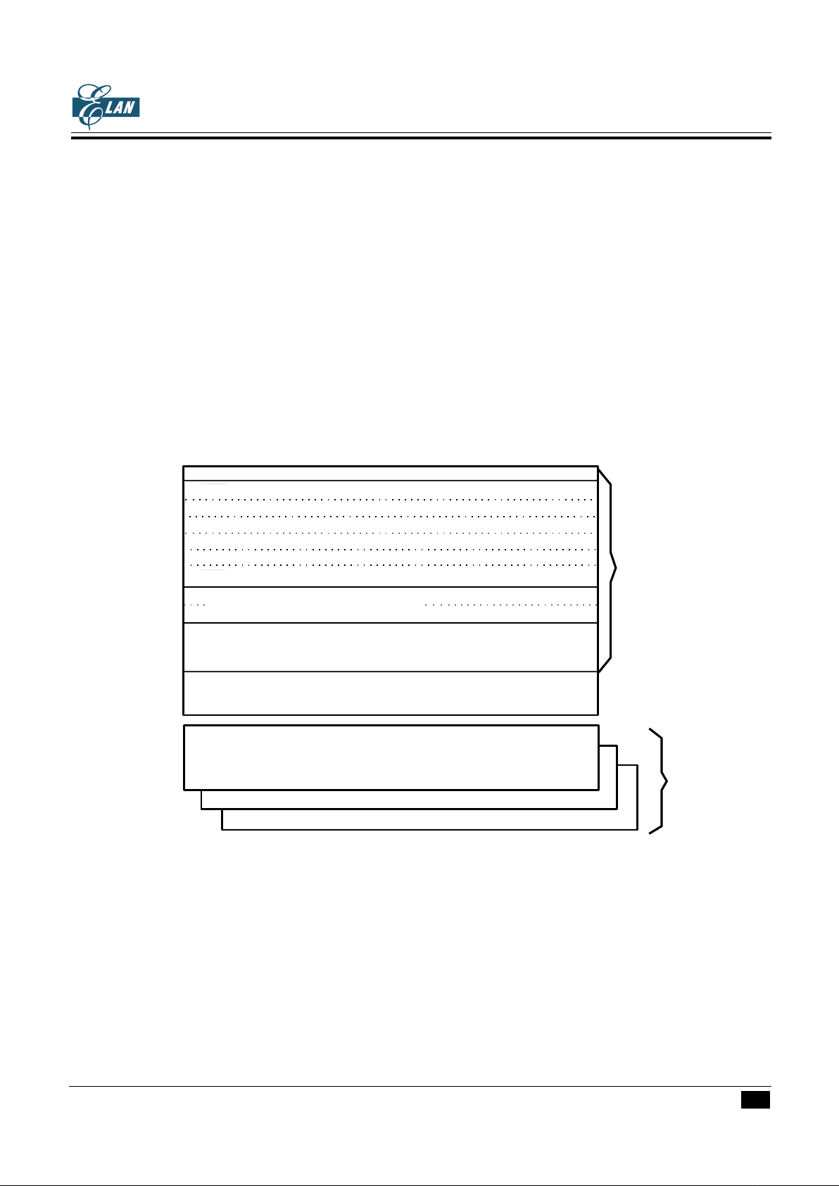
• Operation voltage : 2.2V to 4.8V.
• Clock source : Dual clock system. Low-frequency oscillator is 32 KHz Crystal or RC oscillator
and high-frequency oscillator is a built-in internal oscillator (4.6 MHz).
• Instruction set : 107 powerful instructions.
• Instruction cycle time : 1.7µs for 4.6M Hz (high speed clock).
244µs for 32768 Hz (low speed clock).
• ROM capacity : 16K x 8 bits.
• RAM capacity : 500 x 4 bits.
• Input port : 1 port (P0.0-P0.3), IDLE/STOP releasing function is available by mask option.
(each input pin has a pull-up and pull-down resistor available by mask option).
• Bidrection port : 2 ports (P4, P8). IDLE/STOP release function for P8(0..3) is available by mask
option.
• Built-in watch-dog-timer counter : It is available by mask option.
• 12-bit timer/counter : Two 12-bit timer/counters are programmable for timer, event counter and pulse
width measurement mode.
• Built-in time base counter : 22 stages.
• Subroutine nesting : Up to 13 levels.
• Interrupt : External interrupt . . . . . . 2 input interrupt sources.
Internal interrupt . . . . . . 2 timer overflow interrupts, 1 time base interrupt.
1 speech interrupt.
• LCD driver : 64x16 dots, 1/16 duty, 1/5 bias with voltage multiplier.
• Sound effect : Tone generator and random generator.
• Speech synthesizer : 448K speech data ROM (use as 448K nibbles data ROM).
• PWM or current D/A : Output selection by mask option.
• Power saving function : SLOW, IDLE, STOP operation modes.
• Package type : Chip form 109 pins.
QFP form 160 pins (AQ).
QFP form 128 pins (BQ).
2
* This specification are subject to be changed without notice.
10.8.2001
EM73PA88AEM73PA88A
EM73PA88AEM73PA88A
EM73PA88A
4-BIT MICRO-CONTROLLER FOR LCD PRODUCT4-BIT MICRO-CONTROLLER FOR LCD PRODUCT
4-BIT MICRO-CONTROLLER FOR LCD PRODUCT4-BIT MICRO-CONTROLLER FOR LCD PRODUCT
4-BIT MICRO-CONTROLLER FOR LCD PRODUCT
PreliminaryPreliminary
PreliminaryPreliminary
Preliminary
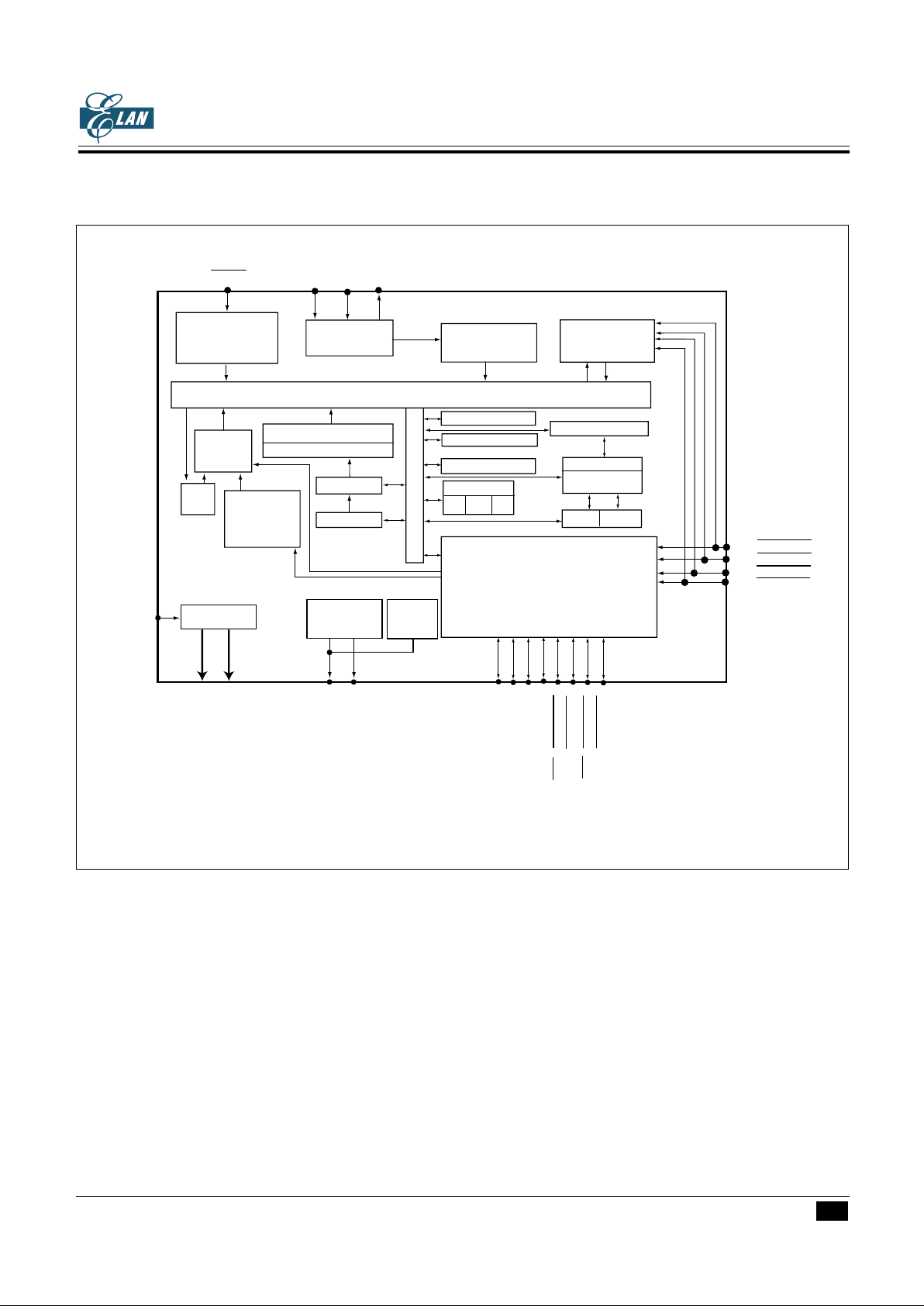
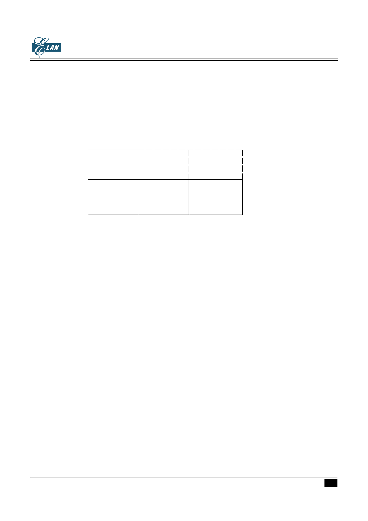
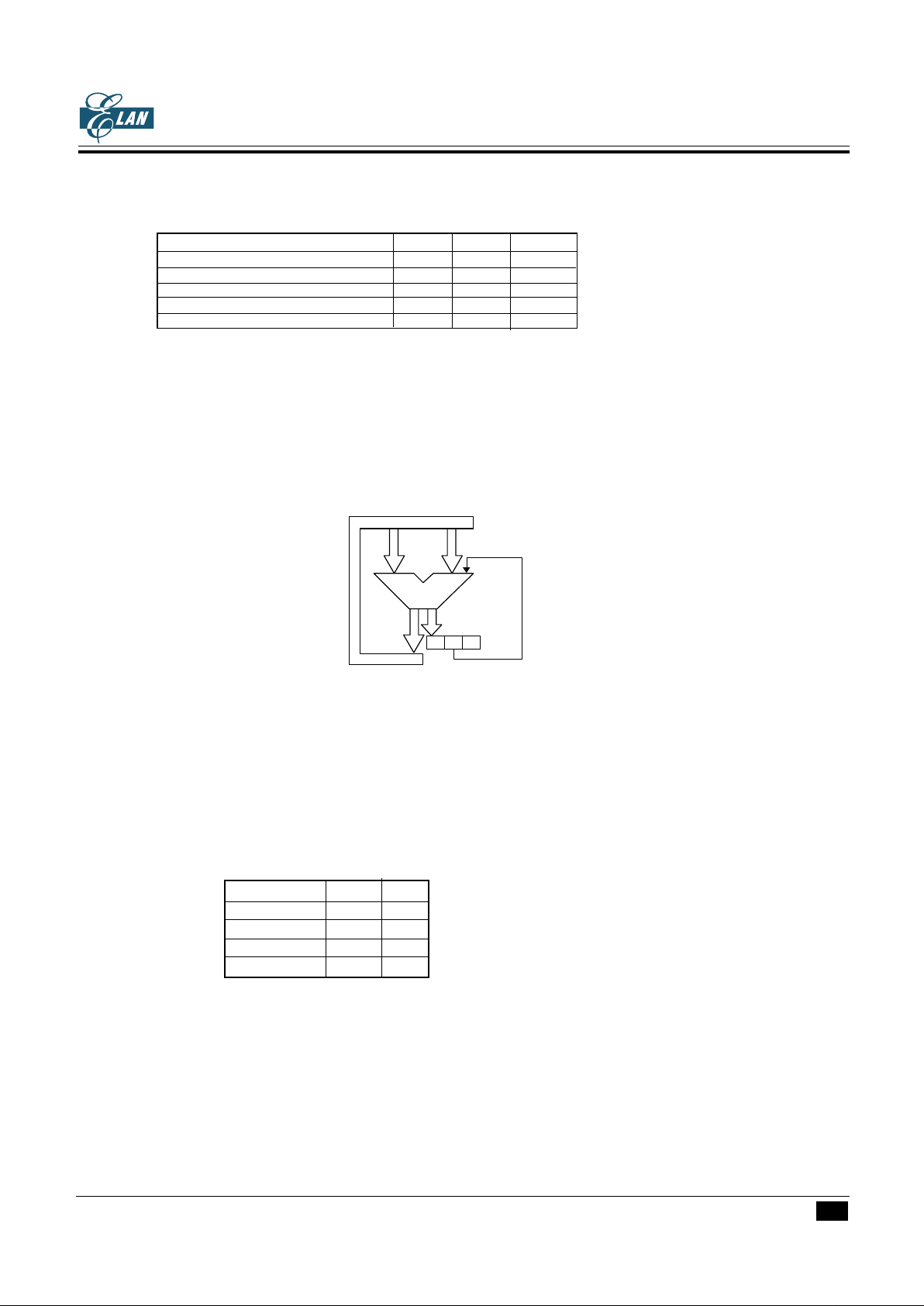
FUNCTION BLOCK DIAGRAMFUNCTION BLOCK DIAGRAM
FUNCTION BLOCK DIAGRAMFUNCTION BLOCK DIAGRAM
FUNCTION BLOCK DIAGRAM
Interrupt
Control
Time
Base
Timer/Counter
(TA,TB)
System Control
Instruction Decoder
Instruction Register
ROM
PC
Data Bus
Reset
Control
Clock
Generator
Timing
Generator
Clock Mode
Control
Data pointer
ACC
ALU
Flag
ZCS
Stack pointer
Stack
RAM
HR
LR
I/O Control
P0.0/WAKEUP0
P0.1/WAKEUP1
P0.2/WAKEUP2
P0.3/WAKEUP3
P4.0
P4.1
P4.2
P4.3
P8.0(INT1)/WAKEUPA
P8.1(TRGB)/WAKEUPB
P8.2(INT0)/WAKEUPC
P8.3(TRGA)/WAKEUPD
RESET
CLK
LXOUT
Speech
synthesizer
LCD Driver
V1~V5
VA,VB
COM0~COM15
BZ1
BZ2
SEG0~SEG63
LXIN
Sound
Generator
3
* This specification are subject to be changed without notice.
EM73PA88AEM73PA88A
EM73PA88AEM73PA88A
EM73PA88A
4-BIT MICRO-CONTROLLER FOR LCD PRODUCT4-BIT MICRO-CONTROLLER FOR LCD PRODUCT
4-BIT MICRO-CONTROLLER FOR LCD PRODUCT4-BIT MICRO-CONTROLLER FOR LCD PRODUCT
4-BIT MICRO-CONTROLLER FOR LCD PRODUCT
10.8.2001
PreliminaryPreliminary
PreliminaryPreliminary
Preliminary
PIN ASSIGNMENTPIN ASSIGNMENT
PIN ASSIGNMENTPIN ASSIGNMENT
PIN ASSIGNMENT
123456789
101112131415161718192021222324252627282930
60
59
58
57
56
55
54
53
52
51
50
49
48
47
46
45
44
43
42
41
110
109
108
107
106
105
104
103
102
101
100
99989796959493929190898887868584838281
141
142
143
144
145
146
147
148
149
150
151
152
153
154
155
156
157
158
159
160
SEG44
SEG43
SEG42
SEG41
SEG40
SEG39
SEG38
SEG37
SEG36
SEG35
SEG34
NC
NC
NC
NC
NC
NC
NC
NC
NC
NGNGNG
SEG33
SEG32
P8.0/DIN
P8.1/DOUT
P8.2
P8.3
P4.0
P4.1
P4.2
P4.3
P0.0/ACLK
P0.1/PGM
P0.2/OE
P0.3/DCLK
VDD2
BZ1
BZ2
VSS
RESET
CLK
VPP
LXIN
LXOUT
VDD
V1V2V3
SEG19
SEG20
SEG21
SEG22
SEG23
SEG24
SEG25
SEG26
SEG27
SEG28
SEG29
NC
NC
NC
NC
NC
NC
NC
NC
NC
SEG62
SEG63
COM15
COM14
COM13
COM12
COM11
COM10
COM9
COM8
COM7
COM6
COM5
COM3
COM2
COM1
COM0
SEG0
SEG1
SEG2
SEG3
SEG4
SEG5
SEG6
SEG7
SEG8NCNC
NC
EM73PA88AAQ
QFP 160
313233343536373839
40
80
79
78
77
76
75
74
73
72
71
70
69
68
67
66
65
64
63
62
61
120
119
118
117
116
115
114
113
112
111
121
122
123
124
125
126
127
128
129
130
131
132
133
134
135
136
137
138
139
140
V4
V5
VA
VB
SEG31
SEG30
NC
NC
NC
NC
SEG9
SEG10
SEG11
SEG12
SEG13
SEG14
SEG15
SEG16
SEG17
SEG18
NC
NC
NC
NC
NC
NC
NC
NC
NC
NC
SEG56
SEG57
SEG58
SEG59
SEG60
SEG61
NCNCNC
SEG55
SEG48
SEG47
SEG46
SEG45
SEG52
SEG51
SEG50
SEG49
NC
NC
SEG54
SEG53
NC
NC
NC
NC
NC
NC
NC
NC
COM4
4
* This specification are subject to be changed without notice.
10.8.2001
EM73PA88AEM73PA88A
EM73PA88AEM73PA88A
EM73PA88A
4-BIT MICRO-CONTROLLER FOR LCD PRODUCT4-BIT MICRO-CONTROLLER FOR LCD PRODUCT
4-BIT MICRO-CONTROLLER FOR LCD PRODUCT4-BIT MICRO-CONTROLLER FOR LCD PRODUCT
4-BIT MICRO-CONTROLLER FOR LCD PRODUCT
PreliminaryPreliminary
PreliminaryPreliminary
Preliminary
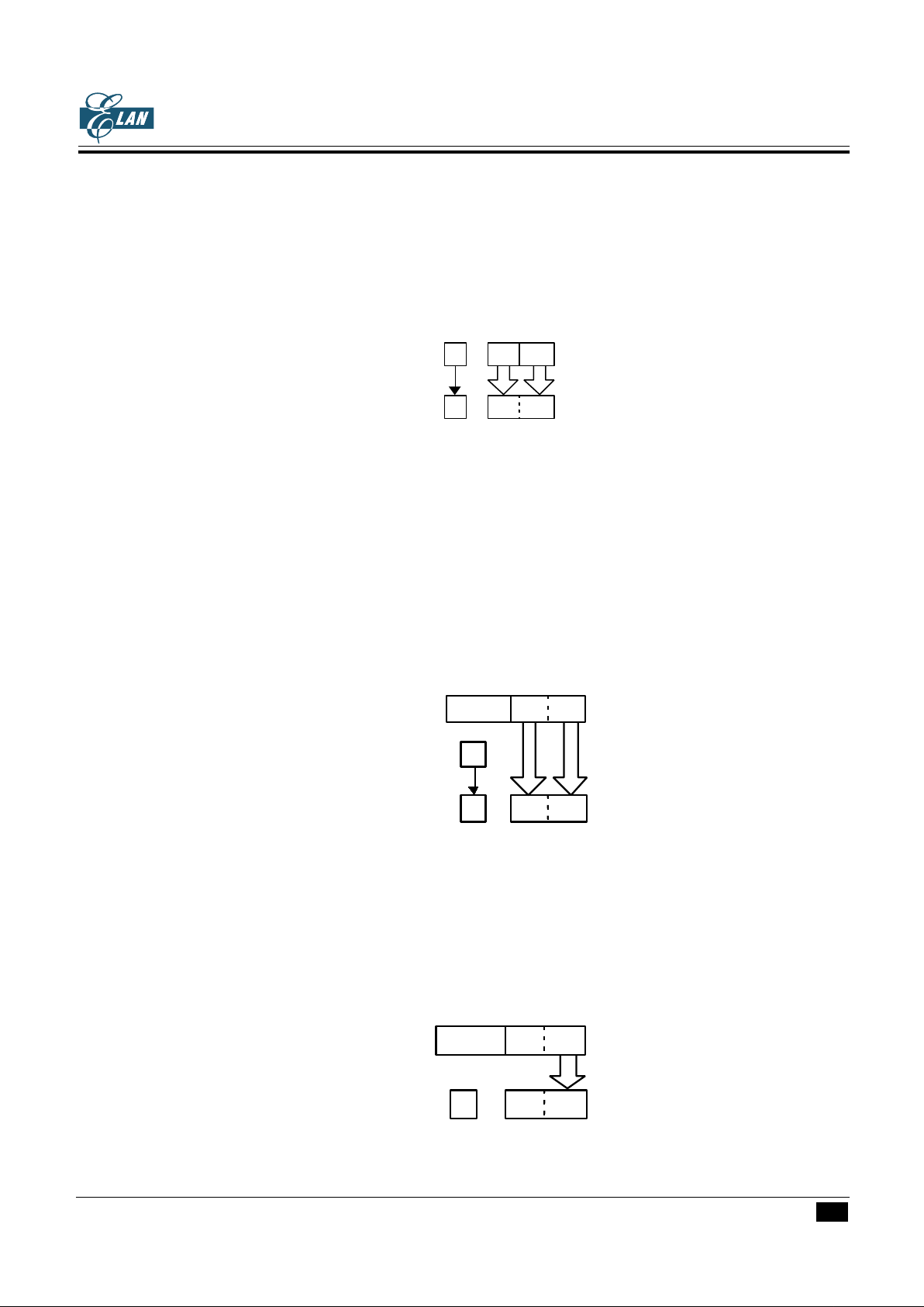
PIN ASSIGNMENTPIN ASSIGNMENT
PIN ASSIGNMENTPIN ASSIGNMENT
PIN ASSIGNMENT
123456789
101112131415161718192021222324252627282930
60
59
58
57
56
55
54
53
52
51
50
49
48
47
46
45
44
43
42
41
102
101
100
99989796959493929190898887868584838281
109
110
111
112
113
114
115
116
117
118
119
120
121
122
123
124
125
126
127
128
NC
NC
NCNCNC
NCNCNC
EM73PA88ABQ
QFP 128
31323334353637
38
64
63
62
61
103
104
105
106
107
108
NCNCNC
NC
NC
NC
NC
40
39
NC
NC
807978777675747372717069686766
65
NC
NC
P8.0/DIN
P8.1/DOUT
P8.2
P8.3
P4.0
P4.1
P4.2
P4.3
P0.0/ACLK
P0.1/PGM
P0.2/OE
P0.3/DCLK
VDD2
BZ1
BZ2
VSS
RESET
CLK
VPP
LXIN
LXOUT
VDD
V1V2V3V4V5
VA
VB
SEG31
SEG32
SEG30
SEG19
SEG20
SEG21
SEG22
SEG23
SEG24
SEG25
SEG26
SEG27
SEG28
SEG29
SEG9
SEG10
SEG11
SEG12
SEG13
SEG14
SEG15
SEG16
SEG17
SEG18
SEG62
SEG63
COM15
COM14
COM13
COM12
COM11
COM10
COM9
COM8
COM7
COM6
COM5
COM3
COM2
COM1
COM0
SEG0
SEG1
SEG2
SEG3
SEG4
SEG5
SEG6
SEG7
SEG8
SEG56
SEG57
SEG58
SEG59
SEG60
SEG61
COM4
SEG44
SEG43
SEG42
SEG41
SEG40
SEG39
SEG38
SEG37
SEG36
SEG35
SEG34
SEG48
SEG47
SEG46
SEG45
SEG52
SEG51
SEG50
SEG49
SEG54
SEG53
SEG55
SEG33
5
* This specification are subject to be changed without notice.
EM73PA88AEM73PA88A
EM73PA88AEM73PA88A
EM73PA88A
4-BIT MICRO-CONTROLLER FOR LCD PRODUCT4-BIT MICRO-CONTROLLER FOR LCD PRODUCT
4-BIT MICRO-CONTROLLER FOR LCD PRODUCT4-BIT MICRO-CONTROLLER FOR LCD PRODUCT
4-BIT MICRO-CONTROLLER FOR LCD PRODUCT
10.8.2001
PreliminaryPreliminary
PreliminaryPreliminary
Preliminary
SymbolSymbol
SymbolSymbol
Symbol
Pin-type Pin-type
Pin-type Pin-type
Pin-type
FunctionFunction
FunctionFunction
Function
VDD Power supply (+).
Power supply (+) for programming OTP.
VDD2 Power supply (+).
VSS Power supply (-).
Power supply (-) for programming OTP.
RESET RESET-A System reset input signal, low active.
Reset input signal for programming OTP.
Always internal pull-up.
CLK OSC-G Capacitor connecting pin for internal high frequency oscillator.
LXIN OSC-B/OSC-H Crystal or RC osc connecting pin for low speed clock source.
LXOUT OSC-B Crystal osc connecting pin for low speed clock source.
P0(0..3)/WAKEUP0..3 INPUT-B 4-bit input port with IDLE/STOP releasing function
P0.0/ACLK : address counter clock for programming OTP.
P0.1/PGMB : program data to OTP cells for programming OTP.
P0.2/OEB : data output enable for programming OTP.
P0.3/DCLK : data in/out clock signal for programming OTP.
mask option : wakeup enable, pull-up
wakeup enable, none
wakeup disable, pull-up
wakeup disable, pull-down
wakeup disable, none
P4(0..3) I/O-O 4-bit bidirection I/O port with high current source.
mask option : open-drain
push-pull, high current PMOS
push-pull, low current PMOS
P8.0(INT1)/WAKEUPA I/O-L 2-bit bidirection I/O port with external interrupt sources input and IDLE
P8.2(INT0)/WAKEUPC /STOP releasing function.
P8.0/DIN : data input for programming OTP.
mask option : wakeup enable, push-pull
wakeup disable, push-pull
wakeup disable, open-drain
P8.1(TRGB)/WAKEUPB I/O-L 2-bit bidirection I/O port with time/counter A,B external input and IDLE
P8.3(TRGA)/WAKEUPD /STOP releasing function.
P8.1/DOUT : data output for programming OTP.
mask option : wakeup enable, push-pull
wakeup disable, push-pull
wakeup disable, open-drain
BZ1 Tone / Speech PWM / D/A output pin.
BZ2 Tone / Speech PWM output pin.
V1, V2, V3, V4, V5, LCD bias pins.
VA, VB
COM0~COM15 LCD common output pins.
SEG0~SEG63 LCD segment output pins.
TEST/VPP Test pin must be floating.
VPP : high voltage (12V) power source for programming OTP.
PIN DESCRIPTIONSPIN DESCRIPTIONS
PIN DESCRIPTIONSPIN DESCRIPTIONS
PIN DESCRIPTIONS
6
* This specification are subject to be changed without notice.
10.8.2001
EM73PA88AEM73PA88A
EM73PA88AEM73PA88A
EM73PA88A
4-BIT MICRO-CONTROLLER FOR LCD PRODUCT4-BIT MICRO-CONTROLLER FOR LCD PRODUCT
4-BIT MICRO-CONTROLLER FOR LCD PRODUCT4-BIT MICRO-CONTROLLER FOR LCD PRODUCT
4-BIT MICRO-CONTROLLER FOR LCD PRODUCT
PreliminaryPreliminary
PreliminaryPreliminary
Preliminary
.
.
.
SCALL, subroutine call entry address
Data table for
[LDAX],[LDAXI]
instruction
Subroutine call entry address
designated by [LCALL a]
instruction
Bank 1
Bank 2
Bank 3
Reset start address
INT0 ; interrupt service routine entry address
TRGA
TRGB
TBI
INT1
0000h
0002h
0004h
0006h
0008h
000Ah
000Ch
000Eh
0086h
07FFh
0800h
0FFFh
1000h
1FFFh
SPI
FUNCTION DESCRIPTIONSFUNCTION DESCRIPTIONS
FUNCTION DESCRIPTIONSFUNCTION DESCRIPTIONS
FUNCTION DESCRIPTIONS
PROGRAM ROM ( 16K X 8 bits )PROGRAM ROM ( 16K X 8 bits )
PROGRAM ROM ( 16K X 8 bits )PROGRAM ROM ( 16K X 8 bits )
PROGRAM ROM ( 16K X 8 bits )
16 K x 8 bits program ROM contains user's program and some fixed data.
The basic structure of the program ROM may be categorized into 5 partitions.
1. Address 0000h: Reset start address.
2. Address 0002h - 000Ch : 6 kinds of interrupt service routine entry addresses.
3. Address 000Eh-0086h : SCALL subroutine entry address, only available at 000Eh, 0016h, 001Eh, 0026h, 002Eh,
0036h, 003Eh, 0046h, 004Eh, 0056h, 005Eh, 0066h, 006Eh, 0076h, 007Eh,0086h.
4. Address 0000h - 07FFh : LCALL subroutine entry address.
5. Address 0000h - 1FFFh : Except used as above function, the other region can be used as user's program and
data region.
address Bank 0 :
7
* This specification are subject to be changed without notice.
EM73PA88AEM73PA88A
EM73PA88AEM73PA88A
EM73PA88A
4-BIT MICRO-CONTROLLER FOR LCD PRODUCT4-BIT MICRO-CONTROLLER FOR LCD PRODUCT
4-BIT MICRO-CONTROLLER FOR LCD PRODUCT4-BIT MICRO-CONTROLLER FOR LCD PRODUCT
4-BIT MICRO-CONTROLLER FOR LCD PRODUCT
10.8.2001
PreliminaryPreliminary
PreliminaryPreliminary
Preliminary
User's program and fixed data are stored in the program ROM. User's program is executed using the PC value
to fetch an instruction code.
The 16Kx8 bits program ROM can be divided into 4 banks. There are 4Kx8 bits per bank.
The program ROM bank is selected by P3(1..0). The program counter is a 13-bit binary counter. The PC
and P3 are initialized to "0" during reset.
When P3(1..0)=00B, the bank0 and bank1 of program ROM will be selected. P3(1..0)=01B, the bank0 and
bank2 will be selected.
Address P3=xx00B P3=xx01B P3=xx10B
0000h
:
: Bank0 Bank0 Bank0
0FFFh
1000h
:
: Bank1 Bank2 Bank3
1FFFh
PROGRAM EXAMPLE :
BANK 0
START: :
:
:
LDIA #00H ; set program ROM to bank1
OUTA P3
B XA1
:
XA : :
:
LDIA #01H ; set program ROM to bank2
OUTA P3
B XB1
:
XB : :
:
LDIA #02H ; set program ROM to bank3
OUTA P3
B XC1
:
XC : :
:
BXD
XD : :
:
:
; - - - - - - - - - - - - - - - - - - - - - - - - - - - - - - - - - - - - - - - - - - - - - - - - - - - - - - - - - - - - - - - - - - - - - - - - - - - - -
BANK 1
XA1 : :
:
BXA
:
XA2 : :

8
* This specification are subject to be changed without notice.
10.8.2001
EM73PA88AEM73PA88A
EM73PA88AEM73PA88A
EM73PA88A
4-BIT MICRO-CONTROLLER FOR LCD PRODUCT4-BIT MICRO-CONTROLLER FOR LCD PRODUCT
4-BIT MICRO-CONTROLLER FOR LCD PRODUCT4-BIT MICRO-CONTROLLER FOR LCD PRODUCT
4-BIT MICRO-CONTROLLER FOR LCD PRODUCT
PreliminaryPreliminary
PreliminaryPreliminary
Preliminary
B XA2
:
; - - - - - - - - - - - - - - - - - - - - - - - - - - - - - - - - - - - - - - - - - - - - - - - - - - - - - - - - - - - - - - - - - - - - - - - - - - - - -
BANK 2
XB1 : :
:
BXB
:
XB2 : :
B XB2
:
; - - - - - - - - - - - - - - - - - - - - - - - - - - - - - - - - - - - - - - - - - - - - - - - - - - - - - - - - - - - - - - - - - - - - - - - - - - - - -
BANK 3
XC1 : :
:
BXC
:
XC2 : :
B XC2
Fixed data can be read out by table-look-up instruction. Table-look-up instruction is requires the Data point
(DP) to indicate the ROM address in obtaining the ROM code data (Except bank 0) :
LDAXLDAX
LDAXLDAX
LDAX
Acc Acc
Acc Acc
Acc
←←
←←
←
ROM[DP] ROM[DP]
ROM[DP] ROM[DP]
ROM[DP]
LL
LL
L
LDAXILDAXI
LDAXILDAXI
LDAXI
Acc Acc
Acc Acc
Acc
←←
←←
←
ROM[DP] ROM[DP]
ROM[DP] ROM[DP]
ROM[DP]
HH
HH
H
,DP+1,DP+1
,DP+1,DP+1
,DP+1
DP is a 12-bit data register that stores the program ROM address as pointer for the ROM code data.
User has to initially load ROM address into DP with instructions "STADPL", and "STADPM, STADPH",
then to obtain the lower nibble of ROM code data by instruction "LDAX" and higher nibble by instruction
"LDAXI"
PROGRAM EXAMPLE: Read out the ROM code of address 1777h by table-look-up instruction.
LDIA #07h;
STADPL ; [DP]L ← 07h
STADPM ; [DP]M ← 07h
STADPH ; [DP]H ← 07h, Load DP=777h
:
LDL #00h;
LDH #03h;
LDAX ; ACC ← 6h
STAMI ; RAM[30] ← 6h
LDAXI ; ACC ← 5h
STAM ; RAM[31] ← 5h
;
ORG 1777h
DATA 56h;
DATA RAM ( 500-nibble ) DATA RAM ( 500-nibble )
DATA RAM ( 500-nibble ) DATA RAM ( 500-nibble )
DATA RAM ( 500-nibble )
A total 500 - nibble data RAM is available from address 000 to 1FFh
Data RAM includes the zero page region, stacks and data areas.
9
* This specification are subject to be changed without notice.
EM73PA88AEM73PA88A
EM73PA88AEM73PA88A
EM73PA88A
4-BIT MICRO-CONTROLLER FOR LCD PRODUCT4-BIT MICRO-CONTROLLER FOR LCD PRODUCT
4-BIT MICRO-CONTROLLER FOR LCD PRODUCT4-BIT MICRO-CONTROLLER FOR LCD PRODUCT
4-BIT MICRO-CONTROLLER FOR LCD PRODUCT
10.8.2001
PreliminaryPreliminary
PreliminaryPreliminary
Preliminary
ZERO- PAGE:
From 000h to 00Fh is the zero-page location. It is used as the zero-page address mode pointer for the
instruction of "STD #k,y; ADD #k,y; CLR y,b; CMP k,y".
PROGRAM EXAMPLE: To write immediate data "07h" to RAM [03] and to clear bit 2 of RAM [0Eh].
STD #07h, 03h ; RAM[03] ← 07h
CLR 0Eh,2 ; RAM[0Eh]2 ← 0
STACK:
There are 13 - level (maximum) stack levels that user can use for subroutine (including interrupt and CALL).
User can assign any level be the starting stack by providing the level number to stack pointer (SP).
When an instruction (CALL or interrupt) is invoked, before enter the subroutine, the previous PC address
is saved into the stack until returned from those subroutines, the PC value is restored by the data saved
in stack.
DATA AREA:
Except the area used by user's application, the whole RAM can be used as data area for storing and loading
general data.
ADDRESSING MODE
The 500 nibble data memory consists of two banks (bank 0 and bank 1). There are 244x4 bits (address
000h~0F3h) in bank 0 and 256x4 bits (address 100h~1FFh) in bank 1.
Increment
Address
020h - 02Fh
0C0h - 0CFh
0D0h - 0DFh
0E0h - 0EFh
Level 0
Level 4
Level 8
Level 12
Level 1
Level 5
Level 9
Level 2
Level 6
Level 10
Level 3
Level 7
Level 11
Increment
Zero-page
000h - 00Fh
010h - 01Fh
0F0h - 0F3h
:
:
:
110h - 11Fh
1E0h - 1EFh
1F0h - 1FFh
100h - 10Fh
:
:
:
Bank 0
Bank 1
10
* This specification are subject to be changed without notice.
10.8.2001
EM73PA88AEM73PA88A
EM73PA88AEM73PA88A
EM73PA88A
4-BIT MICRO-CONTROLLER FOR LCD PRODUCT4-BIT MICRO-CONTROLLER FOR LCD PRODUCT
4-BIT MICRO-CONTROLLER FOR LCD PRODUCT4-BIT MICRO-CONTROLLER FOR LCD PRODUCT
4-BIT MICRO-CONTROLLER FOR LCD PRODUCT
PreliminaryPreliminary
PreliminaryPreliminary
Preliminary
P9.3
instruction field
RAM address
xxxxxxxx
xxxxxxxx
0
instruction field
RAM address
yyyy
0000
yyyy
PROGRAM EXAMPLE: Load the data of RAM address "143h" to RAM address "023h".
SEP P9,3 ; P9.3← 1
LDA 43h ; Acc← RAM[143h]
CLP P9,3 ; P9.3← 0
STA 23h ; RAM[023h]← Acc
(3) Zero-page addressing mode:
The zero-page is in the bank 0 (address 000h~00Fh). The address is the lower 4 bits code of the second byte
in the instruction field.
PROGRAM EXAMPLE: Write immediate "0Fh" to RAM address "005h".
STD #0Fh, 05h ; RAM[05h]← 0Fh
The bank is selected by P9.3. When P9.3 is cleared to "0", the bank 0 is selected. When P9.3 is set to "1", the bank
1 is selected.
The Data Memory consists of three Address mode, namely -
(1) Indirect addressing mode:
The address in the bank is specified by the HL registers.
PROGRAM EXAMPLE: Load the data of RAM address "143h" to RAM address "032h".
SEP P9,3 ; P9.3← 1
LDL #3h ; LR← 3
LDH #4h ; HR← 4
LDAM ; Acc← RAM[134h]
CLP P9,3 ; P9.3← 0
LDL #2h ; LR← 2
LDH #3h ; HR← 3
STAM ; RAM[023h]← Acc
(2) Direct addressing mode:
The address in the bank is directly specified by 8 bits code of the second byte in the instruction field.
P9.3 HR LR
R
AM address
11
* This specification are subject to be changed without notice.
EM73PA88AEM73PA88A
EM73PA88AEM73PA88A
EM73PA88A
4-BIT MICRO-CONTROLLER FOR LCD PRODUCT4-BIT MICRO-CONTROLLER FOR LCD PRODUCT
4-BIT MICRO-CONTROLLER FOR LCD PRODUCT4-BIT MICRO-CONTROLLER FOR LCD PRODUCT
4-BIT MICRO-CONTROLLER FOR LCD PRODUCT
10.8.2001
PreliminaryPreliminary
PreliminaryPreliminary
Preliminary
+2
PROGRAM COUNTER (16K ROM)PROGRAM COUNTER (16K ROM)
PROGRAM COUNTER (16K ROM)PROGRAM COUNTER (16K ROM)
PROGRAM COUNTER (16K ROM)
Program counter ( PC ) is composed by a 13-bit counter, which indicates the next executed address for the
instruction of program ROM instruction.
For BRANCH and CALL instructions, PC is changed by instruction indicating. PC only can indicate the address
from 0000h-1FFFh. The bank number is decided by P3.
(1) Branch instruction:(1) Branch instruction:
(1) Branch instruction:(1) Branch instruction:
(1) Branch instruction:
SBR aSBR a
SBR aSBR a
SBR a
Object code: 00aa aaaa
Condition: SF=1; PC ← PC
12-6.a
( branch condition satisified )
PC Hold original PC value+1 aaaaaa
SF=0; PC← PC +1( branch condition not satisified)
PC Original PC value + 1
LBR aLBR a
LBR aLBR a
LBR a
Object code: 1100 aaaa aaaa aaaa
Condition: SF=1; PC ← PC
12.a
( branch condition satisified )
PC
Hold
a a a a a aaaaaaa
SF=0; PC← PC +2( branch condition not satisified)
PC Original PC value + 2
SLBR aSLBR a
SLBR aSLBR a
SLBR a
Object code: 0101 0101 1100 aaaa aaaa aaaa (a:1000h~1FFFh)
0101 0111 1100 aaaa aaaa aaaa (a:0000h~0FFFh)
Condition: SF=1; PC ← a ( branch condition satisified)
PCaaaaaaaaaaaa a
SF=0 ; PC ← PC + 3 ( branch condition not satisified )
PC Original PC value + 3
(2) Subroutine instruction:(2) Subroutine instruction:
(2) Subroutine instruction:(2) Subroutine instruction:
(2) Subroutine instruction:
SCALL aSCALL a
SCALL aSCALL a
SCALL a
Object code: 1110 nnnn
Condition : PC ← a ; a=8n+6 ; n=1..Fh ; a=86h, n=0
PC00000aaaaa aaa
LCALL aLCALL a
LCALL aLCALL a
LCALL a
Object code: 0100 0aaa aaaa aaaa
Condition: PC ← a
12
* This specification are subject to be changed without notice.
10.8.2001
EM73PA88AEM73PA88A
EM73PA88AEM73PA88A
EM73PA88A
4-BIT MICRO-CONTROLLER FOR LCD PRODUCT4-BIT MICRO-CONTROLLER FOR LCD PRODUCT
4-BIT MICRO-CONTROLLER FOR LCD PRODUCT4-BIT MICRO-CONTROLLER FOR LCD PRODUCT
4-BIT MICRO-CONTROLLER FOR LCD PRODUCT
PreliminaryPreliminary
PreliminaryPreliminary
Preliminary
(3) Interrupt acceptance operation:(3) Interrupt acceptance operation:
(3) Interrupt acceptance operation:(3) Interrupt acceptance operation:
(3) Interrupt acceptance operation:
When an interrupt is accepted, the original PC is pushed into stack and interrupt vector will be loaded into
PC. The interrupt vectors are as follows :
INT0INT0
INT0INT0
INT0 (External interrupt from P8.2)
PC00000000000 1 0
SPISPI
SPISPI
SPI (speech end interrupt)
PC000000000010 0
TRGATRGA
TRGATRGA
TRGA (Timer A overflow interrupt)
PC0000000000 1 1 0
TRGBTRGB
TRGBTRGB
TRGB (Time B overflow interrupt)
PC00000000 0 1 0 0 0
TBI TBI
TBI TBI
TBI (Time base interrupt)
PC00000000 0 1 0 1 0
INT1INT1
INT1INT1
INT1 (External interrupt from P8.0)
PC00000000 0 1 1 0 0
(4) Reset operation:(4) Reset operation:
(4) Reset operation:(4) Reset operation:
(4) Reset operation:
PC00000000000 0 0
PC00aaaaaaaaaa a
RETRET
RETRET
RET
Object code: 0100 1111
Condition: PC ← STACK[SP]; SP + 1
PC The return address stored in stack
RT IRT I
RT IRT I
RT I
Object code: 0100 1101
Condition : FLAG. PC ← STACK[SP]; EI ← 1; SP + 1
PC The return address stored in stack

13
* This specification are subject to be changed without notice.
EM73PA88AEM73PA88A
EM73PA88AEM73PA88A
EM73PA88A
4-BIT MICRO-CONTROLLER FOR LCD PRODUCT4-BIT MICRO-CONTROLLER FOR LCD PRODUCT
4-BIT MICRO-CONTROLLER FOR LCD PRODUCT4-BIT MICRO-CONTROLLER FOR LCD PRODUCT
4-BIT MICRO-CONTROLLER FOR LCD PRODUCT
10.8.2001
PreliminaryPreliminary
PreliminaryPreliminary
Preliminary
(5) Other operations:(5) Other operations:
(5) Other operations:(5) Other operations:
(5) Other operations:
For 1-byte instruction execution: PC + 1
For 2-byte instruction execution: PC + 2
For 3-byte instruction execution: PC + 3
ACCUMULATORACCUMULATOR
ACCUMULATORACCUMULATOR
ACCUMULATOR
Accumulator(ACC) is a 4-bit data register for temporary data storage. For the arithematic, logic and
comparative opertion.., ACC plays a role which holds the source data and result.
FLAGSFLAGS
FLAGSFLAGS
FLAGS
There are three kinds of flag, CF (Carry flag), ZF (Zero flag) and SF (Status flag), these three 1-bit flags
are included by the arithematic, logic and comparative .... operation.
All flags will be put into stack when an interrupt subroutine is served, and the flags will be restored after
RTI instruction is executed.
(1) Carry Flag ( CF )
The carry flag is affected by the following operations:
a. Addition : CF as a carry out indicator, under addition operation, when a carry-out occures, the CF is "1",
likewise, if the operation has no carry-out, CF is "0".
b. Subtraction : CF as a borrow-in indicator, under subtraction operation, when a borrow occures, the CF
is "0", likewise, if there is no borrow-in, the CF is "1".
c. Comparision: CF as a borrow-in indicator for Comparision operation as in the subtraction operation.
d. Rotation: CF shifts into the empty bit of accumulator for the rotation and holds the shift out data after
rotation.
e. CF test instruction : Under TFCFC instruction, the CF content is sent into SF then clear itself as "0".
Under TTSFC instruction, the CF content is sent into SF then set itself as "1".
(2) Zero Flag ( ZF )
ZF is affected by the result of ALU, if the ALU operation generates a "0" result, the ZF is "1",
likewise, the ZF is "0".
(3) Status Flag ( SF )
The SF is affected by instruction operation and system status.
a. SF is initiated to "1" for reset condition.
b. Branch instruction is decided by SF, when SF=1, branch condition is satisified, likewise, when SF = 0,
branch condition is unsatisified.
14
* This specification are subject to be changed without notice.
10.8.2001
EM73PA88AEM73PA88A
EM73PA88AEM73PA88A
EM73PA88A
4-BIT MICRO-CONTROLLER FOR LCD PRODUCT4-BIT MICRO-CONTROLLER FOR LCD PRODUCT
4-BIT MICRO-CONTROLLER FOR LCD PRODUCT4-BIT MICRO-CONTROLLER FOR LCD PRODUCT
4-BIT MICRO-CONTROLLER FOR LCD PRODUCT
PreliminaryPreliminary
PreliminaryPreliminary
Preliminary
PROGRAM EXAMPLE:
Check following arithematic operation for CF, ZF, SF
CF ZF SF
LDIA #00h; - 1 1
LDIA #03h; - 0 1
ADDA #05h; - 0 1
ADDA #0Dh; - 0 0
ADDA #0Eh; - 0 0
ALUALU
ALUALU
ALU
The arithematic operation of 4 - bit data is performed in ALU unit . There are 2 flags that can be affected by
the result of ALU operation, ZF and SF. The operation of ALU is affected by CF only.
ALU STRUCTUREALU STRUCTURE
ALU STRUCTUREALU STRUCTURE
ALU STRUCTURE
ALU supported user arithematic operation functions, including Addition, Subtraction and Rotaion.
ALU FUNCTIONALU FUNCTION
ALU FUNCTIONALU FUNCTION
ALU FUNCTION
(1) Addition:
ALU supports addition function with instructions ADDAM, ADCAM, ADDM #k, ADD #k,y .... .
The addition operation affects CF and ZF. Under addition operation, if the result is "0", ZF will be "1",
otherwise, ZF will be "0", When the addition operation has a carry-out. CF will be "1", otherwise, CF will
be "0".
EXAMPLE:
Operation Carry Zero
3+4=7 0 0
7+F=6 1 0
0+0=0 0 1
8+8=0 1 1
(2) Subtraction:
ALU supports subtraction function with instructions SUBM #k, SUBA #k, SBCAM, DECM... . The
subtraction operation affects CF and ZF. Under subtraction operation, if the result is negative, CF will
be "0", and a borrow out, otherwise, if the result is positive, CF will be "1". For ZF, if the result of subtraction
operation is "0", the ZF is "1", likewise, ZF is "1".
ZF CF SF
ALU
DATA BUS
 Loading...