

ELAN EM73P968 Datasheet

EM73P968
4-BIT MICRO-CONTROLLER FOR LCD PRODUCT
GENERAL DESCRIPTION
EM73P968 is an advanced single chip CMOS 4-bit one time programming (OTP) micro-controller. It contains
16K-byte ROM, 2.5K nibbles RAM, 4-bit ALU, 13-level subroutine nesting, 22-stage time base, two 12-bit timer/
counters for the kernel function. EM73P968 also contains 6 interrupt sources, 1 input port, 8 bidirection ports, Max
LCD display (52x5), built-in watch-dog-timer and high speed Timer/Counter.
An analog to digital (A/D) converter having 8-bit multipler analog input and 8-bit resolution. Serial peripheral
interface (SPI).
EM73P968 has plentiful operating modes (SLOW, IDLE, STOP) intended to reduce the power consumption.
FEATURES
Operation voltage : 2.2V ~ 6V.
Clock source : Dual clock system. Low-frequency oscillator is Crystal or RC oscillator (32K Hz,
Instruction set : 107 powerful instructions.
Instruction cycle time : Up to 2us for 4 MHz (high speed clock).
ROM capacity : 16K x 8 bits.
RAM capacity : 2.5K x 4 bits.
Input port : 1 port, P0(0..3), IDLE/STOP releasing function are available by mask option.
Output port : 9 pins (P17.0, P30, P31), P17.0, P30, P31 are shared with LCD pins.
Bidirection port : 9 ports (P1, P2, P4, P5, P6, P7, P8, P11, P15). IDLE/STOP releasing function are
12-bit timer/counter : Two 12-bit timer/counters are programmable for timer, event counter and pulse width
A/D converter : An analog to digital (A/D) converter having 8-bit multipler analog input and 8-bit
SPI : Serial peripheral interface.
Built-in watch-dog-timer : It is available by mask option.
Built-in time base counter : 22 stages.
Built-in high Speed Timer/Counter : Could be timer.
Subrountine nesting : Up to 13 levels.
Interrupt : External . . . . . 2 input interrupt sources.
LCD driver : 52 X 5 dots, 1/3 bias, 1/4 or 1/5 duty by mask option.
Power saving function : SLOW, IDLE, STOP operation mode.
Package type : Chip form.
Preliminary
connect an external resistor) by mask option and high-frequency oscillator is RC
(Connect an external resistor) or Crystall oscillator.
122 µs for 32768 Hz (low speed clock with frequency Double)
available by mask option for P8(0..3), P5 and P6 have high current sink.
measurement.
resolution.
Internal . . . . . . 2 Timer overflow interrupts, 1 time base interrupt.
1 high speed counter overflow interrupt.
QFP 128 pin.
APPLICATIONS
EM73P968 is suitable for application in family applicance, consumer products, hand held games, calculator and
the toy controller.
* This specification are subject to be changed without notice.
8.14.2001
1
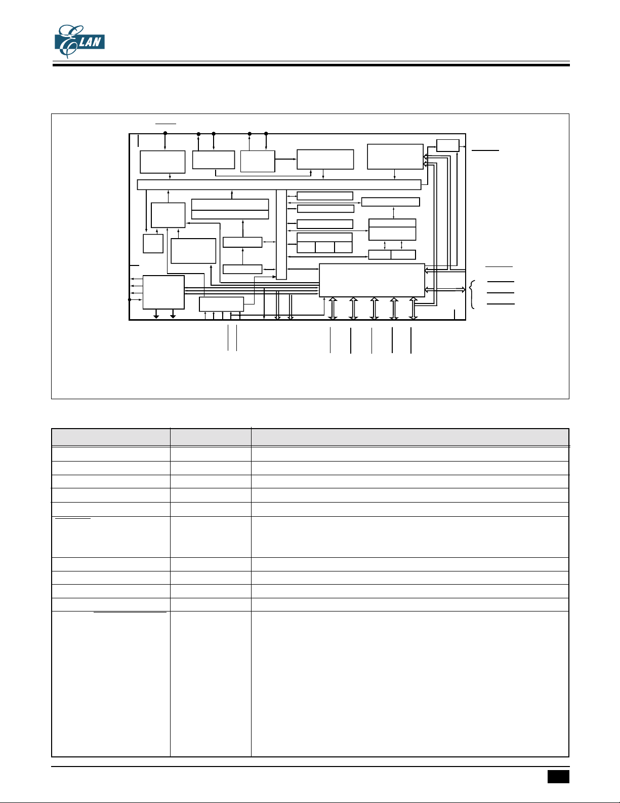
FUNCTION BLOCK DIAGRAM
EM73P968
4-BIT MICRO-CONTROLLER FOR LCD PRODUCT
Preliminary
TEST
V
RLC
LXIN
LXOUT
Clock
Generator
(slow)
System Control
Data Bus
ROM
PC
P17.0/COM4
P30/SEG(44~47)
(AIN 0~3)P6/WAKEUP
(AIN 4~7)P7/WAKEUP
Timing
Generator
Data pointer
ACC
ALU
Flag
ZCS
P31/SEG(48~51)
P1/WAKEUP
Stack pointer
HR
I/O Control
P11/WAKEUP
Sleep Mode
Control
Stack
RAM
LR
P15.2/WAKEUP
P15.3/WAKEUP
P8/WAKEUP
SPI
VSS
P15.0/P15.1/
WAKEUP
P0/WAKEUP
/WAKEUP
P2
/WAKEUP
P4
/WAKEUP
P5
Generator
(TA,TB)
XINXOUT
Clock
Instruction Decoder
Instruction Register
ADC
Vref
VAD
VADSS
RESET
VDD
Reset
Control
Interrupt
Control
Time
Timer/Counter
Base
V1
V2
V3
LCD
SEG0~SEG43
COM0~COM3
PIN DESCRIPTIONS
Symbol Pin-type Function
V
DD
V
SS
Vref ADC power (+)
V
AD
V
ADSS
RESET RESET-A System reset input signal, low active
XIN/RC
OSC OSC-A/OSC-H1 Crystal/RC clock source connecting pin
XOUT OSC-A Crystal connecting pin
LXIN OSC-B/OSC-H2 Crystal/RC connecting pin for low speed clock source
LXOUT OSC-B Crystal connecting pin for low speed clock source
P0(0..3)/WAKEUP(0..3) INPUT-K 4-bit input port with IDLE/STOP releasing function
Power supply (+)
Power supply (-)
ADC power (+)
ADC power (-)
mask option : none
pull-up
P0.0/ACLK : address counter clock for programming OTP.
P0.1/PGMB : program data to OTP cells for programming OTP.
P0.2/OEB : data output enable for programming OTP.
P0.3/DCLK : data in/out clock signal for programming OTP.
mask option 1 : wakeup disable
wakeup enable
mask option 2 : low current pull up
normal current pull up
high current pull up
none
* This specification are subject to be changed without notice.
8.14.2001
2
EM73P968
4-BIT MICRO-CONTROLLER FOR LCD PRODUCT
Preliminary
PIN DESCRIPTIONS
Symbol Pin-type Function
P8.0(INT1)/WAKEUPA I/O-R1 2-bit bidirection I/O port with external interrupt sources input and IDLE/
/DIN STOP releasing function
P8.2(INT0)/WAKEUPC P8.0/DIN : data input for programming OTP
mask option 1 : wakeup disable
wakeup enable
mask option 2 : low current push pull
normal current push pull
high current push pull
none
P8.1(TRGB)/WAKEUPB, I/O-R1 2-bit bidirection I/O port with timer/counter A, B external input and
/DOUT IDLE/STOP releasing function
P8.3(TRGA)/WAKEUPD P8.1/DOUT : data output for programming OTP
mask option 1 : wakeup disable
wakeup enable
mask option 2 : low current push pull
normal current push pull
high current push pull
none
P6(0..3)/WAKEUP(20..23) I/O-R1 8-bit bidirection I/O port with IDLE/STOP releasing function.
AIN (0..3) Share with A/D analog input pin.
P7(0..3)/WAKEUP(24..27) mask option 1 : wakeup disable
AIN (4..7) wakeup enable
mask option 2 : low current push pull
normal current push pull
high current push pull
none
P4(0..3)/WAKEUP(12,15) I/O-R1 4-bit bidirection I/O port with IDLE/STOP releasing function
mask option 1 : wakeup disable
wakeup enable
mask option 2 : low current push pull
normal current push pull
high current push pull
none
* This specification are subject to be changed without notice.
8.14.2001
3
EM73P968
4-BIT MICRO-CONTROLLER FOR LCD PRODUCT
Preliminary
PIN DESCRIPTIONS
Symbol Pin-type Function
P1(0..3)/WAKEUP(4..7) I/O-R1 18-bit bidirection I/O pins with IDLE/STOP releasing function
P2(0..3)/WAKEUP(8..11) mask option 1 : wakeup disable
P5(0..3)/WAKEUP(16..19) wakeup enable
P11(0..3)/ mask option 2 : low current push pull
WAKEUP(28..31) normal current push pull
P15.2/P15.3/ high current push pull
WAKEUP(34,35) none
P15.0/WAKEUP(32) 1-bit bidirection I/O pins with IDLE/STOP releasing function. Share with
SPI data input/output pin.
mask option 1 : wakeup disable
wakeup enable
mask option 2 : low current push pull
normal current push pull
high current push pull
none
P15.1/WAKEUP(33) I/O-R1 1-bit bidirection I/O pins with IDLE/STOP releasing function.Share with
SPI clock input/output pin.
mask option 1 : wakeup disable
wakeup enable
mask option 2 : low current push pull
normal current push pull
high current push pull
none
P17.0/COM4 Output-L 1-bit output pin with LCD common pin
mask option : LCD common pin
Push pull
Open-drain
P30(0..3)/SEG(51..48) Output-M 8-bit output pins are shared with LCD segment pin
P31(0..3)/SEG(47..44) mask option : LCD segment pin
Low current push pull
Normal current push pull
High current push pull
Open drain
COM0~COM3 LCD common output pins
SEG0~SEG43 LCD segment output pins
VRLC, V1, V2, V3 -- LCD bias voltage pins
TEST -- Test pin must be connected to VSS
VPP : high voltage (12V) power source for programming OTP
* This specification are subject to be changed without notice.
8.14.2001
4
* This specification are subject to be changed without notice.
SEG40
SEG41
127
128
SEG38
SEG39
125
126
SEG36
SEG37
123
124
SEG34
SEG35
121
122
SEG32
SEG33
119
120
SEG30
SEG31
117
118
SEG29
SEG28
115
116
SEG26
SEG27
113
114
SEG24
SEG25
111
112
NC
110
NC
109
NC
108
NC
107
NC
106
NC
105
NC
104
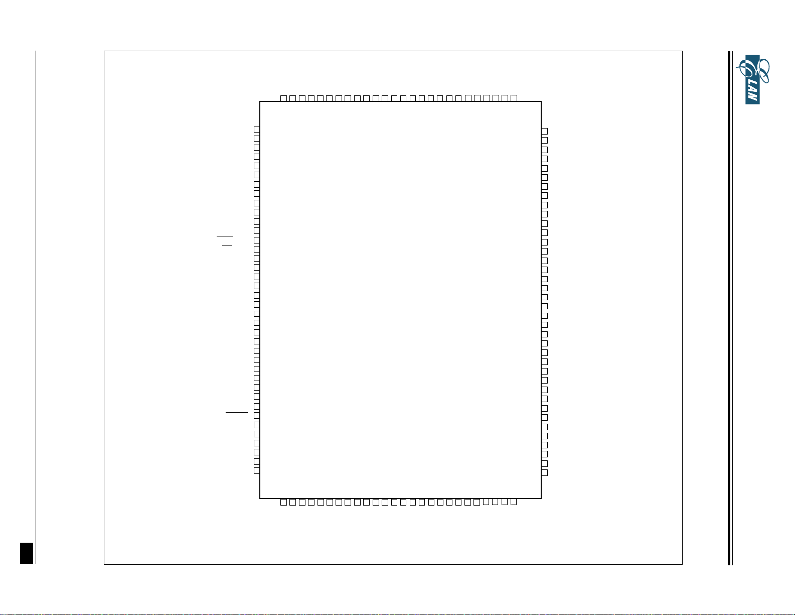
PIN ASSIGNMENT
SEG23
103
8.14.2001
SEG42
SEG43
SEG44
SEG45
SEG46
SEG47
SEG48
SEG49
SEG50
SEG51
VPP
ACLK/P0.0
PGM/P0.1
OE/P0.2
DCLK/P0.3
P1.0
P1.1
P1.2
P1.3
P2.0
P2.1
P2.2
P2.3
P4.0
P4.1
P4.2
P4.3
P5.0
P5.1
P5.2
P5.3
RESET
P6.0
P6.1
P6.2
P6.3
P7.0
P7.1
1
2
3
4
5
6
7
8
9
10
11
12
13
14
15
16
17
18
19
20
21
22
23
24
25
26
27
28
29
30
31
32
33
34
35
36
37
38
49
48
47
46
45
44
43
42
41
40
39
XIN
VSS
P8.3
P8.2
DOUT/P8.1
DIN/P8.0
VAD
VREF
VADSS
P7.3
P7.2
EM73P968
QFP 128
55
54
53
52
51
50
VR1
LXOUT
VDDC
LXIN
VSS
XOUT
VDDI
62
61
60
59
58
57
56
NC
NC
NC
VR2
NC
NC
63
NC
64
NC
102
101
100
SEG22
SEG21
SEG20
99
SEG19
98
SEG18
97
SEG17
SEG16
96
95
SEG15
94
SEG14
93
SEG13
92
SEG12
91
SEG11
90
SEG10
89
SEG9
88
SEG8
87
SEG7
86
SEG6
85
SEG5
84
SEG4
83
SEG3
82
SEG2
81
SEG1
80
SEG0
79
COM4
78
COM3
77
COM2
76
COM1
75
COM0
74
P15.3
73
P15.2
72
P15.1
71
P15.0
70
P11.3
69
P11.2
68
P11.1
67
P11.0
66
VRLC
65
VR3
Preliminary
4-BIT MICRO-CONTROLLER FOR LCD PRODUCT
EM73P968
5
4-BIT MICRO-CONTROLLER FOR LCD PRODUCT
Preliminary
FUNCTION DESCRIPTIONS
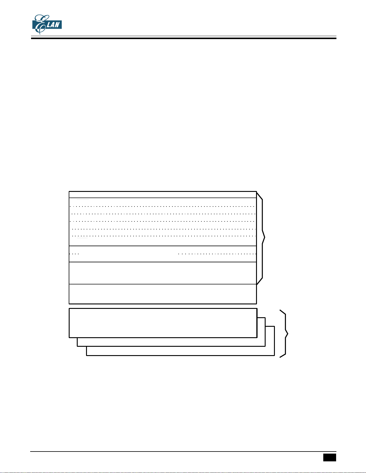
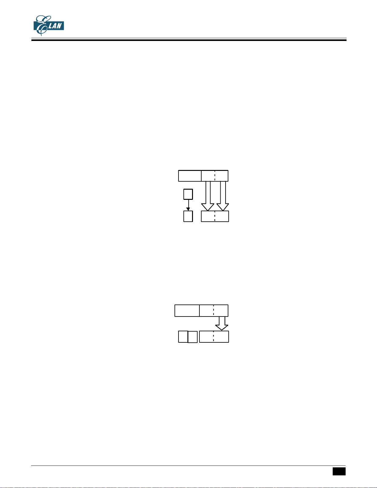
PROGRAM ROM ( 16K X 8 bits )
16 K x 8 bits program ROM contains user's program and some fixed data.
The basic structure of the program ROM may be categorized into 5 partitions.
1. Address 0000h : Reset start address.
2. Address 0002h - 000Ch : 6 kinds of interrupt service routine entry addresses.
3. Address 000Eh - 0086h : SCALL subroutine entry address, only available at 000Eh, 0016h, 001Eh, 0026h, 002Eh,
0036h, 003Eh, 0046h, 004Eh, 0056h, 005Eh, 0066h, 006Eh, 0076h, 007Eh, 0086h.
4. Address 0000h - 07FFh : LCALL subroutine entry address.
5. Address 0000h - 1FFFh : Except used as above function, the other region can be used as user's program and
data region.
address Bank 0 :
EM73P968
0000h
0002h
0004h
0006h
0008h
000Ah
000Ch
000Eh
0086h
.
.
.
07FFh
0800h
0FFFh
1000h
1FFFh
Reset start address
INT0 ; interrupt service routine entry address
HTCI / ADI
TRGA
TRGB
TBI
INT1
SCALL, subroutine call entry address
Bank 1
Bank 2
Bank 3
Subroutine call entry address
designated by [LCALL a]
instruction
Data table for
[LDAX],[LDAXI]
instruction
* This specification are subject to be changed without notice.
8.14.2001
6
EM73P968
4-BIT MICRO-CONTROLLER FOR LCD PRODUCT
User's program and fixed data are stored in the program ROM. User's program is executed using the PC value
Preliminary
to fetch an instruction code.
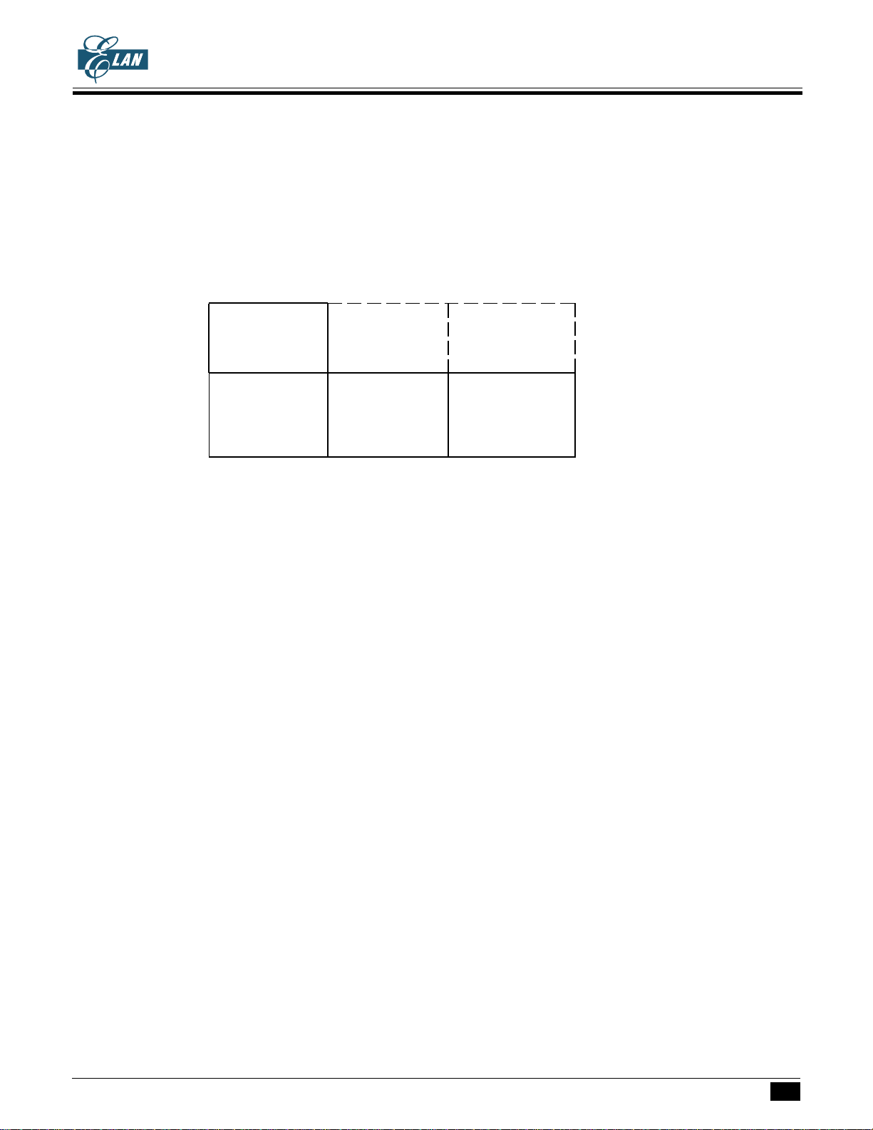
The 16Kx8 bits program ROM can be divided into 4 banks. There are 4Kx8 bits per bank.
The program ROM bank is selected by P3(1..0). The program counter is a 13-bit binary counter. The PC and
P3 are initialized to "0" during reset.
When P3(1..0)=00B, the bank0 and bank1 of program ROM will be selected. P3(1..0)=01B, the bank0 and
bank2 will be selected.
P3=xx00B
Address P3=xx11B P3=xx01B P3=xx10B
0000h
:
: Bank0 Bank0 Bank0
0FFFh
1000h
:
: Bank1 Bank2 Bank3
1FFFh
PROGRAM EXAMPLE:
BANK 0
START: :
:
:
LDIA #00H ; set program ROM to bank1
OUTA P3
B XA1
:
XA : :
:
LDIA #01H ; set program ROM to bank2
OUTA P3
B XB1
:
XB : :
:
LDIA #02H ; set program ROM to bank3
OUTA P3
B XC1
:
XC : :
:
BXD
XD : :
:
:
; - - - - - - - - - - - - - - - - - - - - - - - - - - - - - - - - - - - - - - - - - - - - - - - - - - - - - - - - - - - - - - - - - - - - - - - - - - - - - - - - - - - - - -
BANK 1
XA1 : :
:
BXA
:
XA2 : :
* This specification are subject to be changed without notice.
8.14.2001
7

EM73P968
4-BIT MICRO-CONTROLLER FOR LCD PRODUCT
B XA2
Preliminary
:
; - - - - - - - - - - - - - - - - - - - - - - - - - - - - - - - - - - - - - - - - - - - - - - - - - - - - - - - - - - - - - - - - - - - - - - - - - - - - -
BANK 2
XB1 : :
:
BXB
:
XB2 : :
B XB2
:
; - - - - - - - - - - - - - - - - - - - - - - - - - - - - - - - - - - - - - - - - - - - - - - - - - - - - - - - - - - - - - - - - - - - - - - - - - - - - -
BANK 3
XC1 : :
:
BXC
:
XC2 : :
B XC2
Fixed data can be read out by table-look-up instruction. Table-look-up instruction is requires the Data point
(DP) to indicate the ROM address in obtaining the ROM code data (Except bank 0) :
LDAX Acc
LDAXI Acc
←←
← ROM[DP]
←←
←←
← ROM[DP]
←←
L
,DP+1
H
DP is a 12-bit data register that stores the program ROM address as pointer for the ROM code data.
User has to initially load ROM address into DP with instructions "STADPL", and "STADPM, STADPH",
then to obtain the lower nibble of ROM code data by instruction "LDAX" and higher nibble by instruction
"LDAXI".
PROGRAM EXAMPLE: Read out the ROM code of address 1777h by table-look-up instruction.
LDIA #07h;
STADPL ; [DP]
STADPM ; [DP]
STADPH ; [DP]
:
LDL #00h;
LDH #03h;
LDAX ; ACC ← 6h
STAMI ; RAM[30] ← 6h
LDAXI ; ACC ← 5h
STAM ; RAM[31] ← 5h
;
ORG 1777h
DATA 56h;
← 07h
L
← 07h
M
← 07h, Load DP=777h
H
DATA RAM ( 2548-nibble )
A total 2548 - nibble data RAM is available from address 000 to 9FFh
Data RAM includes the zero page region, stacks and data areas.
* This specification are subject to be changed without notice.
8.14.2001
8
EM73P968
4-BIT MICRO-CONTROLLER FOR LCD PRODUCT
Preliminary
Bank 0 Address 0 1 2 3 4 56789ABCDEF
P9=0000B 000-00Fh ZERO PAGE
010-01Fh
020-02Fh COM0
030-03Fh COM1
040-04Fh COM2
050-05Fh COM3
060-06Fh COM4
070-07Fh
080-08Fh
090-09Fh
0A0-0AFh
0B0-0BFh
0C0-0CFh Level 0 Level 1 Level 2 Level 3
0D0-0DFh Level 4 Level 5 Level 6 Level 7
0E0-0EFh Level 8 Level 8 Level 10 Level 11
0F0-0FFh Level 12 TCA TCB DP SPW
Bank 1
P9=0001B 100-10Fh
:
:
1F0-1FFh
Bank 2
P9=0010B 200-20Fh
:
:
2F0-2FFh
Bank 3
P9=0011B 300-30Fh
:
:
3F0-3FFh
Bank 9
P9=1001B 900-90Fh
:
:
9F0-9FFh
:
:
:
:
:
:
:
* This specification are subject to be changed without notice.
8.14.2001
9
EM73P968
4-BIT MICRO-CONTROLLER FOR LCD PRODUCT
Preliminary
ZERO- PAGE:
From 000h to 00Fh is the zero-page location. It is used as the zero-page address mode pointer for the
instruction of "STD #k,y; ADD #k,y; CLR y,b; CMP k,y".
PROGRAM EXAMPLE: To write immediate data "07h" to RAM [03] and to clear bit 2 of RAM [0Eh].
STD #07h, 03h ; RAM[03] ← 07h
CLR 0Eh,2 ; RAM[0Eh]
STACK:
There are 13 - level (maximum) stack levels that user can use for subroutine (including interrupt and CALL).
User can assign any level be the starting stack by providing the level number to stack pointer (SP).
When an instruction (CALL or interrupt) is invoked, before enter the subroutine, the previous PC address
is saved into the stack until returned from those subroutines, the PC value is restored by the data saved in stack.
DATA AREA:
← 0
2
Except the area used by user's application, the whole RAM can be used as data area for storing and loading
general data.
ADDRESSING MODE
The 2548 nibble data memory consists of ten banks (bank 0 ~ bank 9). There are 244x4 bits (address
000h~0F3h) in bank 0 and 2304x4 bits (address 100h ~ 9FF) in bank 1 ~ bank 9.
The bank is selected by P9.
P9(3..0) Initial value : 0 0 0 0
RBK Bank RAM address(hex)
0 0 0 0 0 0 0 0 ~ 0 F F
0 0 0 1 1 1 0 0 ~ 1 F F
0 0 1 0 2 2 0 0 ~ 2 F F
0 0 1 1 3 3 0 0 ~ 3 F F
0 1 0 0 4 4 0 0 ~ 4 F F
0 1 0 1 5 5 0 0 ~ 5 F F
0 1 1 0 6 6 0 0 ~ 6 F F
0 1 1 1 7 7 0 0 ~ 7 F F
1 0 0 0 8 8 0 0 ~ 8 F F
1 0 0 1 9 9 0 0 ~ 9 F F
1 0 1 0~ 0 0 0 0 ~ 0 F F
1 1 1 1
The Data Memory consists of three Address mode, namely -
(1) Indirect addressing mode:
The address in the bank is specified by the HL registers.
* This specification are subject to be changed without notice.
P9(3,2,1,0)
RAM address
HR LR
8.14.2001
10
4-BIT MICRO-CONTROLLER FOR LCD PRODUCT
Preliminary
PROGRAM EXAMPLE: Load the data of RAM address "143h" to RAM address "032h".
OUT #0001B,P9 ; RAM bank1
LDL #3h ; LR← 3
LDH # 4h ; HR ← 4
LDAM ; Acc← RAM[134h]
OUT #0000B,P9 ; RAM bank0
LDL #2h ; LR← 2
LDH # 3h ; HR ← 3
STAM ; RAM[023h]← Acc
(2) Direct addressing mode:
The address in the bank is directly specified by 8 bits code of the second byte in the instruction field.
instruction field
xxxxxxxx
P9(3..0)
EM73P968
RAM address
PROGRAM EXAMPLE: Load the data of RAM address "143h" to RAM address "023h".
OUT #0001B,P9
LDA 43h ; Acc← RAM[143h]
OUT #0001B,P9
STA 23h ; RAM[023h]← Acc
(3) Zero-page addressing mode:
The zero-page is in the bank 0 (address 000h~00Fh). The address is the lower 4 bits code of the second byte
in the instruction field.
xxxxxxxx
instruction field
yyyy
RAM address
PROGRAM EXAMPLE: Write immediate "0Fh" to RAM address "005h".
STD #0Fh, 05h ; RAM[05h]← 0Fh
00 00
0000
yyyy
* This specification are subject to be changed without notice.
8.14.2001
11
EM73P968
4-BIT MICRO-CONTROLLER FOR LCD PRODUCT
PROGRAM COUNTER (16K ROM)
Preliminary
Program counter ( PC ) is composed by a 13-bit counter, which indicates the next executed address for the
instruction of program ROM instruction.
For BRANCH and CALL instructions, PC is changed by instruction indicating. PC only can indicate the address
from 0000h-1FFFh. The bank number is decided by P3.
(1) Branch instruction:
SBR a
Object code: 00aa aaaa
Condition: SF=1; PC ← PC
( branch condition satisified )
12-6.a
PC Hold original PC value+1 aaaaaa
SF=0; PC← PC +1( branch condition not satisified )
PC Original PC value + 1
LBR a
Object code: 1100 aaaa aaaa aaaa
Condition: SF=1; PC ← PC
( branch condition satisified )
12.a
Hold
PC
a a a a a a aaaaaa
+2
SF=0; PC← PC +2( branch condition not satisified )
PC Original PC value + 2
SLBR a
Object code: 0101 0101 1100 aaaa aaaa aaaa (a:1000h~1FFFh)
0101 0111 1100 aaaa aaaa aaaa (a:0000h~0FFFh)
Condition: SF=1; PC ← a ( branch condition satisified )
PCaaaaaaaaaaaa a
SF=0 ; PC ← PC + 3 ( branch condition not satisified )
PC Original PC value + 3
(2) Subroutine instruction:
SCALL a
Object code: 1110 nnnn
Condition : PC ← a ; a=8n+6 ; n=1..Fh ; a=86h, n=0
PC00000aaaaa aaa
LCALL a
Object code: 0100 0aaa aaaa aaaa
Condition: PC ← a
* This specification are subject to be changed without notice.
8.14.2001
12
EM73P968
4-BIT MICRO-CONTROLLER FOR LCD PRODUCT
Preliminary
PC00aaaaaaaaaa a
RET
Object code: 0100 1111
Condition: PC ← STACK[SP]; SP + 1
PC The return address stored in stack
RT I
Object code: 0100 1101
Condition : FLAG. PC ← STACK[SP]; EI ← 1; SP + 1
PC The return address stored in stack
(3) Interrupt acceptance operation:
When an interrupt is accepted, the original PC is pushed into stack and interrupt vector will be loaded into
PC. The interrupt vectors are as follows :
INT0 (External interrupt from P8.2)
PC00000000000 1 0
TRGH (High speed counter interrupt)
PC000000000010 0
TRGA (Timer A overflow interrupt)
PC0000000000 1 1 0
TRGB (Time B overflow interrupt)
PC00000000 0 1 0 0 0
TBI (Time base interrupt)
PC00000000 0 1 0 1 0
INT1 (External interrupt from P8.0)
PC00000000 0 1 1 0 0
(4) Reset operation:
PC00000000000 0 0
* This specification are subject to be changed without notice.
8.14.2001
13

EM73P968
4-BIT MICRO-CONTROLLER FOR LCD PRODUCT
Preliminary
(5) Other operations:
For 1-byte instruction execution: PC + 1
For 2-byte instruction execution: PC + 2
For 3-byte instruction execution: PC + 3
ACCUMULATOR
Accumulator(ACC) is a 4-bit data register for temporary data storage. For the arithematic, logic and
comparative opertion.., ACC plays a role which holds the source data and result.
FLAGS
There are three kinds of flag, CF (Carry flag), ZF (Zero flag) and SF (Status flag), these three 1-bit flags
are included by the arithematic, logic and comparative .... operation.
All flags will be put into stack when an interrupt subroutine is served, and the flags will be restored after
RTI instruction is executed.
(1) Carry Flag ( CF )
The carry flag is affected by the following operations:
a. Addition : CF as a carry out indicator, under addition operation, when a carry-out occures, the CF is "1",
likewise, if the operation has no carry-out, CF is "0".
b. Subtraction : CF as a borrow-in indicator, under subtraction operation, when a borrow occures, the CF
is "0", likewise, if there is no borrow-in, the CF is "1".
c. Comparision : CF as a borrow-in indicator for Comparision operation as in the subtraction operation.
d. Rotation : CF shifts into the empty bit of accumulator for the rotation and holds the shift out data after
rotation.
e. CF test instruction : Under TFCFC instruction, the CF content is sent into SF then clear itself as "0".
Under TTSFC instruction, the CF content is sent into SF then set itself as "1".
(2) Zero Flag ( ZF )
ZF is affected by the result of ALU, if the ALU operation generates a "0" result, the ZF is "1", likewise, the
ZF is "0".
(3) Status Flag ( SF )
The SF is affected by instruction operation and system status.
a. SF is initiated to "1" for reset condition.
b. Branch instruction is decided by SF, when SF=1, branch condition is satisified, likewise, when SF = 0,
branch condition is unsatisified.
* This specification are subject to be changed without notice.
8.14.2001
14
EM73P968
4-BIT MICRO-CONTROLLER FOR LCD PRODUCT
PROGRAM EXAMPLE:
Preliminary
Check following arithematic operation for CF, ZF, SF
CF ZF SF
LDIA #00h; - 1 1
LDIA #03h; - 0 1
ADDA #05h; - 0 1
ADDA #0Dh; - 0 0
ADDA #0Eh; - 0 0
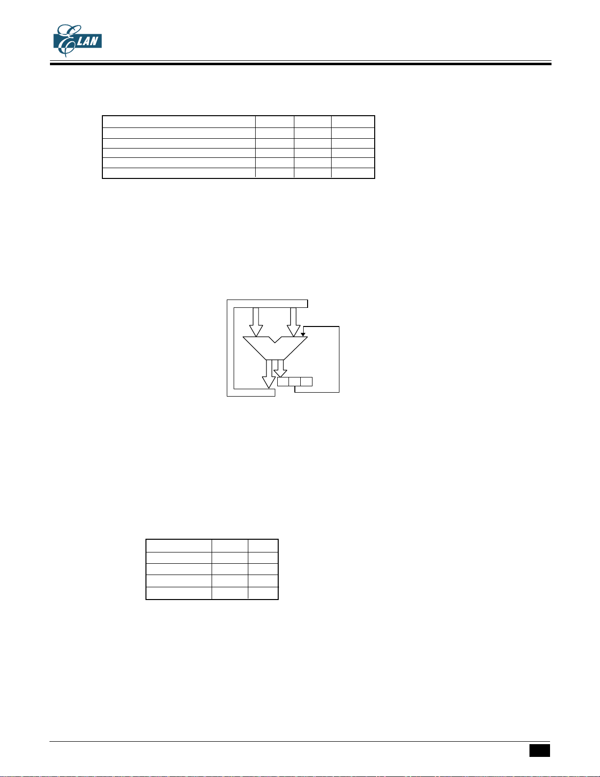
ALU
The arithematic operation of 4-bit data is performed in ALU unit. There are 2 flags that can be affected by
the result of ALU operation, ZF and SF. The operation of ALU is affected by CF only.
ALU STRUCTURE
ALU supported user arithematic operation functions, including Addition, Subtraction and Rotaion.
DATA BUS
ALU
ZF CF SF
ALU FUNCTION
(1) Addition:
ALU supports addition function with instructions ADDAM, ADCAM, ADDM #k, ADD #k,y .... .
The addition operation affects CF and ZF. Under addition operation, if the result is "0", ZF will be "1",
otherwise, ZF will be "0". When the addition operation has a carry-out, CF will be "1", otherwise, CF will
be "0".
EXAMPLE:
Operation Carry Zero
3+4=7 0 0
7+F=6 1 0
0+0=0 0 1
8+8=0 1 1
(2) Subtraction:
ALU supports subtraction function with instructions SUBM #k, SUBA #k, SBCAM, DECM... . The
subtraction operation affects CF and ZF. Under subtraction operation, if the result is negative, CF will
be "0", and a borrow out, otherwise, if the result is positive, CF will be "1". For ZF, if the result of subtraction
operation is "0", the ZF is "1", likewise, ZF is "1".
* This specification are subject to be changed without notice.
8.14.2001
15
EM73P968
4-BIT MICRO-CONTROLLER FOR LCD PRODUCT
EXAMPLE:
Preliminary
Operation Carry Zero
8-4=4 1 0
7-F= -8(1000) 0 0
9-9=0 1 1
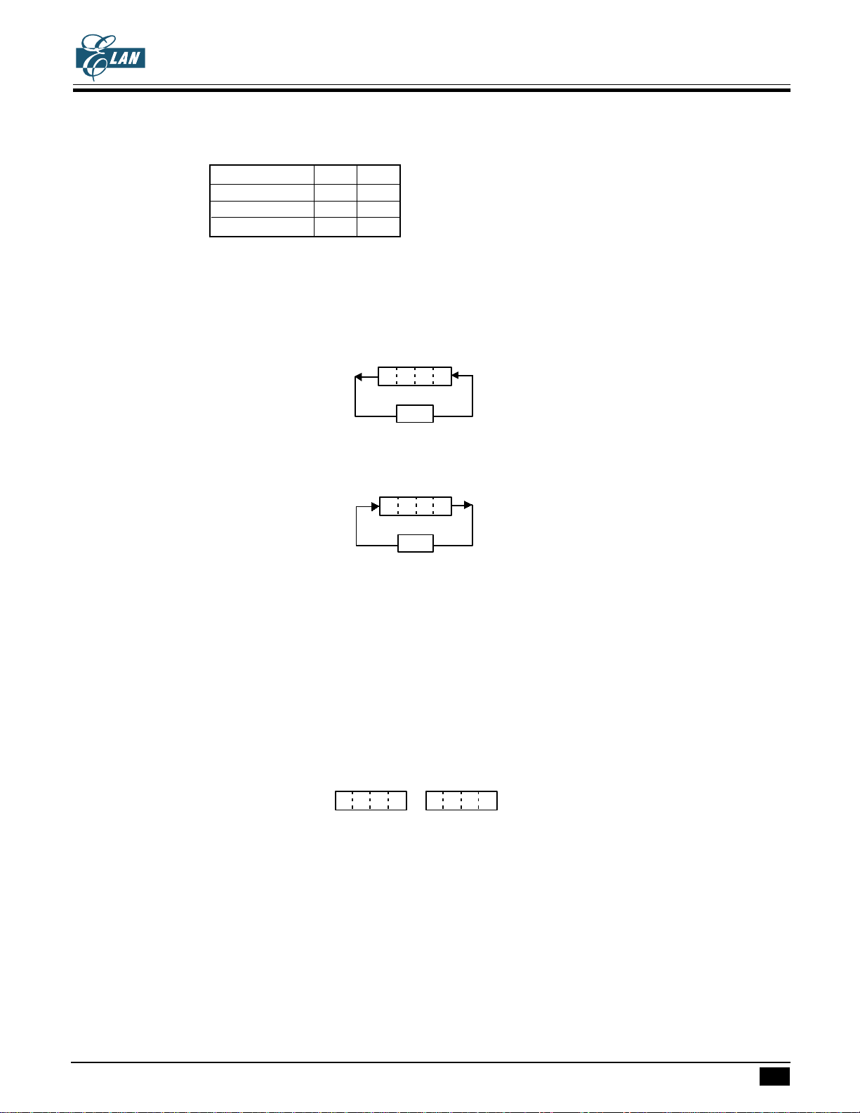
(3) Rotation:
Two types of rotation operation are available, one is rotation left, the other is rotation right.
RLCA instruction rotates Acc value counter-clockwise, shift the CF value into the LSB bit of Acc and hold
the shift out data in CF.
MSB LSB
ACC
CF
RRCA instruction operation rotates Acc value clockwise, shift the CF value into the MSB bit of Acc and
hold the shift out data in CF.
MSB LSB
ACC
CF
PROGRAM EXAMPLE: To rotate Acc clockwise (right) and shift a "1" into the MSB bit of Acc.
TTCFS; CF ← 1
RRCA; rotate Acc right and shift CF=1 into MSB.
HL REGISTER
HL register are two 4-bit registers, they are used as a pair of pointer for the RAM memoryaddress. They are
used as also 2 independent temporary 4-bit data registers. For certain instructions, L register can be a pointer
to indicate the pin number (Port4 only).
HL REGISTER STRUCTURE
3 2 1 0
H REGISTER
3 2 1 0
L REGISTER
HL REGISTER FUNCTION
(1) HL register is used as a temporary register for instructions : LDL #k, LDH #k, THA, THL, INCL, DECL,
EXAL, EXAH.
PROGRAM EXAMPLE:
LDL #05h;
LDH #0Dh;
Load immediate data "5h" into L register, "0Dh" into H register.
(2) HL register is used as a pointer for the address of RAM memory for instructions : LDAM, STAM, STAMI ..
PROGRAM EXAMPLE: Store immediate data "#0Ah" into RAM of address 35h.
* This specification are subject to be changed without notice.
8.14.2001
16
 Loading...