

ELAN EM73P362CQ, EM73P362BQ Datasheet

GENERAL DESCRIPTIONGENERAL DESCRIPTION
GENERAL DESCRIPTION
GENERAL DESCRIPTIONGENERAL DESCRIPTION
EM73P362 is an advanced single chip CMOS 4-bit one-time-programmable (OTP) micro-controller. It contains
3K-byte ROM, 52-nibble RAM, 4-bit ALU, 13-level subroutine nesting, 22-stage time base, one 12-bit timer for
the kernal function and one high speed counter. EM73P362 also contains 5 interrupt sources, 1 input port, 4
bidirection ports, built-in watch-dog-timer and LCD driver (27x3 to 15x3).
Except low-power consumption and high speed, EM73P362 has the STOP mode and IDLE mode operation for
power saving function.
FEATURESFEATURES
FEATURES
FEATURESFEATURES
• Operation voltage : 1.3V to 1.8V. (clock frequency : 32K Hz)
• Clock source : Single clock system for crystal, connect a external resistor or external clock
• Instruction set : 109 powerful instructions.
• Instruction cycle time : Up to 122µs for 32 K Hz.
• ROM capacity : 3072 x 8 bits.
• RAM capacity : 52 x 4 bits.
• Input port : 1 port (4-bit).
• Bidirection port : 4 ports (P4, P6, P7, P8) are available by mask option. P4 is a high current port.
• 12-bit timer : One 12-bit timer is programmable for timer.
• High speed counter : The high speed counter includes one 8-bit high speed counter, one 12-bit general
• Built-in time base counter: 22 stages.
• Subrountine nesting : Up to 13 levels.
• Interrupt : External interrupt . . . . . .2 input interrupt sources.
• LCD driver : 27x3 to 15x3 dots available by mask option. 1/3, 1/2 and static three kinds of duty
• Built-in watch-dog-timer is available by mask option.
• Built-in low battery detector.
• Power saving function : STOP mode and IDLE mode.
• Package type : Chip form 50 pins.
EM73P362EM73P362
EM73P362
EM73P362EM73P362
4-BIT MICRO-CONTROLLER FOR LCD PRODUCT4-BIT MICRO-CONTROLLER FOR LCD PRODUCT
4-BIT MICRO-CONTROLLER FOR LCD PRODUCT
4-BIT MICRO-CONTROLLER FOR LCD PRODUCT4-BIT MICRO-CONTROLLER FOR LCD PRODUCT
source, available by mask option.
(P4.0 and TONE available by mask option. P4.1~P4.3 are shared with the input/
output of RFO.) P6, P7 and P8 are shared with SEG15-SEG26.
counter and a resistor frequency oscillator. It has resistor to frequency oscillation
mode, melody mode and auto load timer mode.
Internal interrupt . . . . . . 2 timer overflow interrupts,
1 time base interrupt.
(1/2 bias) selectable. The programming method of LCD driver is RAM mapping.
QFP 52 pins (CQ).
QFP 100 pins (BQ).
*
This specification are subject to be changed without notice.
11.1.2001
1
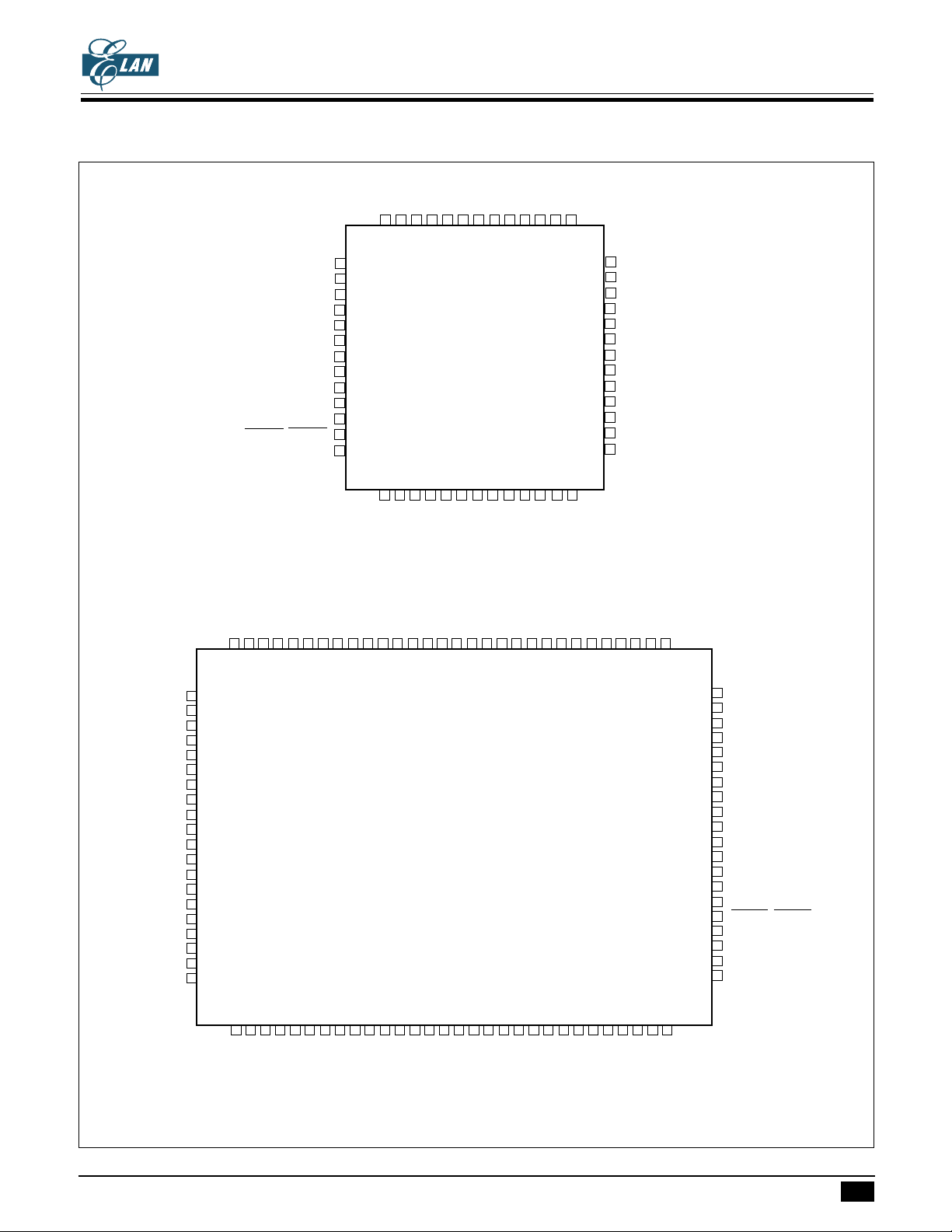
PIN ASSIGNMENTPIN ASSIGNMENT
PIN ASSIGNMENT
PIN ASSIGNMENTPIN ASSIGNMENT
COM1
COM0
VEE
VB
VA
(VSS)VSS
XIN
XOUT
(VDD)VDD
VEE2
BAT
(RESET)RESET
(ACLK)P0.0
NCNCSEG0
525150
1
2
3
4
5
6
EM73P362CQ
7
8
9
10
11
12
13
EM73P362EM73P362
EM73P362
EM73P362EM73P362
4-BIT MICRO-CONTROLLER FOR LCD PRODUCT4-BIT MICRO-CONTROLLER FOR LCD PRODUCT
4-BIT MICRO-CONTROLLER FOR LCD PRODUCT
4-BIT MICRO-CONTROLLER FOR LCD PRODUCT4-BIT MICRO-CONTROLLER FOR LCD PRODUCT
SEG2
SEG3
SEG4
SEG5
SEG6
SEG7
SEG8
SEG9
SEG1
48
47464544434241
49
QFP 52
SEG10
40
39
38
37
36
35
34
33
32
31
30
29
28
27
SEG11
SEG12
SEG13
SEG14
P8.0
P8.1
P8.2
P8.3
P7.0
P7.1
P7.2
P7.3
P6.0
NC
NC
NC
NC
SEG14
SEG13
SEG12
SEG11
SEG10
SEG9
SEG8
SEG7
SEG6
SEG5
SEG4
SEG3
NC
NC
NC
NC
141516171819202122
P4.0
TONE
(OEB)P0.2
(PGMB)P0.1
NCNCNCNCNCNCNCNCP8.0
8079787776757473727170696867666564636261605958575655545352
81
82
83
84
85
86
87
88
89
90
91
92
93
94
95
96
97
98
99
100
123456789
P8.1
P8.2
P8.3
P7.0
EM73P362BQ
QFP 100
101112131415161718192021222324252627282930
(DIN)P4.1
(DCLK)P0.3
P7.1
P7.2
P7.3
(DOUT)P4.2
P6.0
P6.1
24
26
25
P6.3
P6.1
P6.2
COM2
COM2NCNCNCNCNCNCNCNC
P4.3
(VPP)VPP
P6.2
P6.3
23
NC
51
50
49
48
47
46
45
44
43
42
41
40
39
38
37
36
35
34
33
32
31
NC
NC
NC
NC
NC
VPP(VPP)
P4.3
P4.2(DOUT)
P4.1(DIN)
P4.0
SOUND
P0.3(DCLK)
P0.2(OEB)
P0.1(PGMB)
P0.0(ACLK)
RESET(RESET)
NC
NC
NC
NC
NCNCNCNCNCNCNC
NC
SEG2
SEG1
SEG0
COM1
VEE
COM0
VB
VA
LXIN
(GND)GND
Remark : In ( ) pin used for OTP programming.
*
This specification are subject to be changed without notice.
VEE2
LXOUT
(VDD)VDD
NCNCNCNCNCNCNC
BAT
NC
11.1.2001
2
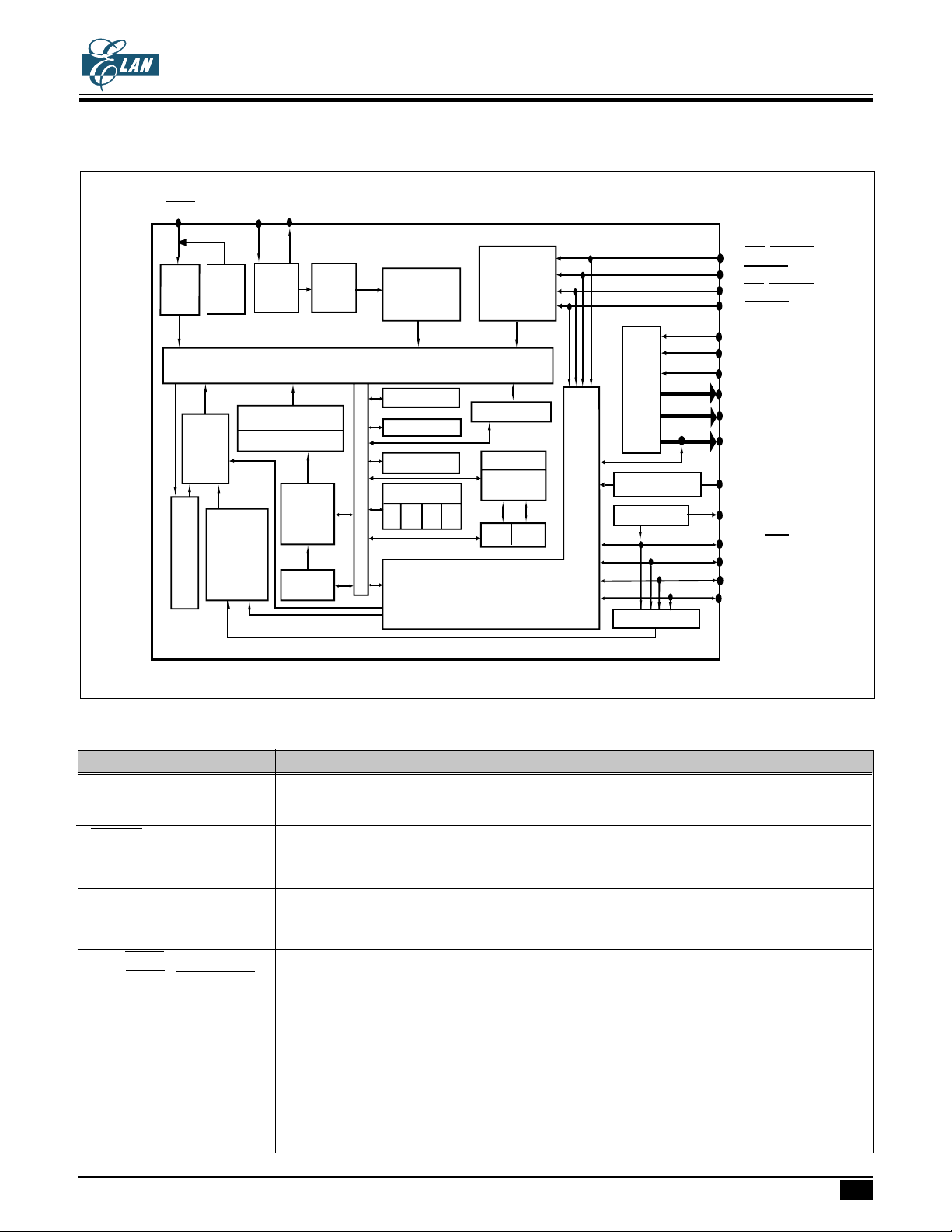
FUNCTION BLOCK DIAGRAMFUNCTION BLOCK DIAGRAM
FUNCTION BLOCK DIAGRAM
FUNCTION BLOCK DIAGRAMFUNCTION BLOCK DIAGRAM
EM73P362EM73P362
EM73P362
EM73P362EM73P362
4-BIT MICRO-CONTROLLER FOR LCD PRODUCT4-BIT MICRO-CONTROLLER FOR LCD PRODUCT
4-BIT MICRO-CONTROLLER FOR LCD PRODUCT
4-BIT MICRO-CONTROLLER FOR LCD PRODUCT4-BIT MICRO-CONTROLLER FOR LCD PRODUCT
RESET
Reset
Control
Interrupt
Control
Time
Base
XOUT
XIN
WDT
Clock
Generator
Instruction Decoder
Instruction Register
12-bit
timer
(TA)
Frequency
doubler
System Control
ROM
PC
Data pointer
Data Bus
ZCS G
Timing
Generator
ACC
ALU
Flag
Sleep Mode
Control
Stack pointer
Stack
RAM
HR
LR
I/O Control
P0.0(INT1)/WAKEUP0
P0.1/WAKEUP1
P0.2(INT0)/WAKEUP2
P0.3/WAKEUP3
VA
VB
LCD
driver
Low battery detector
Tone generator
High speed counter
VEE
COM0~COM2
SEG0~SEG14
P6,P7,P8/SEG(26..15)
BAT
TONE
P4.0(RX)/TONE
P4.1(CS)
P4.2(RY)
P4.3(RZ)
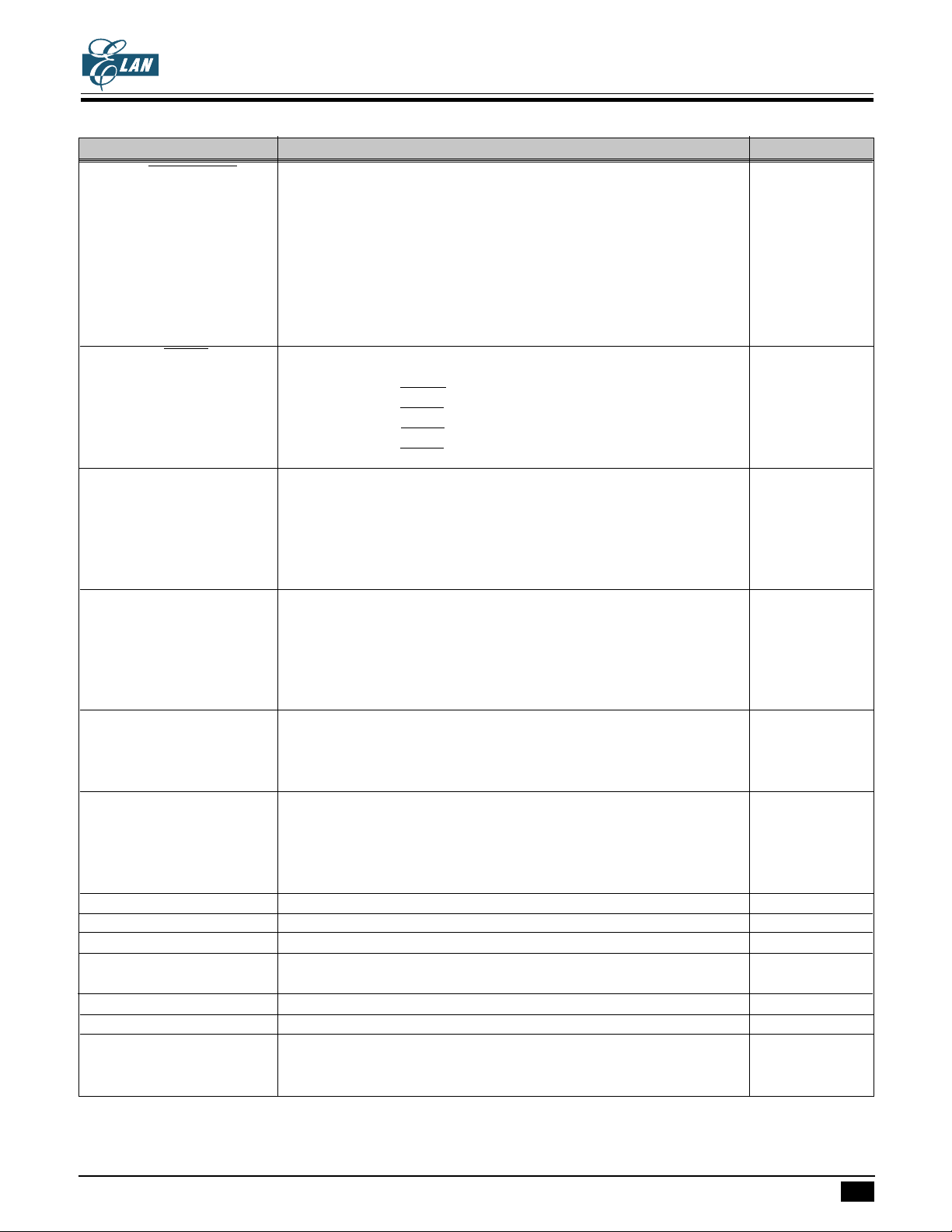
PIN DESCRIPTIONSPIN DESCRIPTIONS
PIN DESCRIPTIONS
PIN DESCRIPTIONSPIN DESCRIPTIONS
Pin name Function PIN type
VDD Power supply (+), Power supply (+) for programming OTP
VSS Power supply (-), Power supply (-) for programming OTP
RESET System reset input signal, low active RESET_A
mask option : none
pull-up
XIN Crystal / external resistor or external clock source OSC_A / OSC_F
connecting pin
XOUT Crystal / external resistor connecting pin OSC_A / OSC_F
P0.0(INT1)/WAKEUP0, 2-bit input pins with external interrupt sources input INPUT_J
P0.2(INT0)/WAKEUP2 and STOP/IDLE releasing function
mask option : wake-up enable, pull-up
wakeup enable, none
wakeup disable, pull-up
wakeup disable, pull-down
wakeup disable, none
In programming OTP mode:
P0.0/ACLK : address counter clock for programming OTP
P0.2/OEB : data output enable for programming OTP
*
This specification are subject to be changed without notice.
11.1.2001
3
EM73P362EM73P362
EM73P362
EM73P362EM73P362
4-BIT MICRO-CONTROLLER FOR LCD PRODUCT4-BIT MICRO-CONTROLLER FOR LCD PRODUCT
4-BIT MICRO-CONTROLLER FOR LCD PRODUCT
4-BIT MICRO-CONTROLLER FOR LCD PRODUCT4-BIT MICRO-CONTROLLER FOR LCD PRODUCT
PIN DESCRIPTIONSPIN DESCRIPTIONS
PIN DESCRIPTIONS
PIN DESCRIPTIONSPIN DESCRIPTIONS
Pin name Function P
P0(1,3)/WAKEUP1,3 2-bit input pins with STOP / IDLE releasing function INPUT_H
mask option : wakeup enable, pull-up
wakeup enable, none
wakeup disable, pull-up
wakeup disable, pull-down
wakeup disable, none
In programming OTP mode :
P0.1/PGMB : program data to OTP cells for programming OTP
P0.3/DCLK : data in/out clock signal for programming OTP
P4.0(RX)/TONE 1-bit bidirection I/O pin or inverse sound effect output or I/O_O
RF oscillation
mask option : TONE enable, push-pull, high current PMOS
TONE disable, open-drain(apply to RF oscillation)
TONE disable, push-pull, high current PMOS
TONE disable, push-pull, low current PMOS
P4.1(CS) 1-bit bidirection I/O pin or RF oscillation bias pin I/O_X
mask option : open-drain(apply to RF oscillation)
push-pull, high current PMOS
push-pull, low current PMOS
In programming OTP mode :
P4.1/DIN : data input for programming OTP
P4.2(RY) 1-bit bidirection I/O pins or RF oscillation input pins I/O_Y
mask option : open-drain(apply to RF oscillation)
push-pull, high current PMOS
push-pull, low current PMOS
In programming OTP mode :
P4.2/DOUT : data output for programming OTP
P4.3(RZ) 1-bit bidirection I/O pins or RF oscillation input pins I/O_Y
mask option : open-drain(apply to RF oscillation)
push-pull, high current PMOS
push-pull, low current PMOS
P6(0..3)/SEG(23..26), 12-bit bidirection I/O pins are shared with LCD segment pin I/O_O
P7(0..3)/SEG(19..22), mask option : segment enable, open-drain
P8(0..3)/SEG(15..18) segment disable, open-drain
segment disable, push-pull, high current PMOS
segment disable, push-pull, low current PMOS
BAT Connect the capacitor for built-in low battery detector
TONE Built-in tone generator output
VA, VB, VEE Connect the capacitors for LCD bias voltage
VEE2 Used for LCD bias voltage
Connect to VDD
COM0 ~ COM2 LCD common output pins
SEG0 ~ SEG14 LCD segment output pins
VPP In normal mode : No connection (Floating)
In programming OTP mode :
VPP : high voltage (12V) power source for programming OTP
IN type
*
This specification are subject to be changed without notice.
11.1.2001
4
4-BIT MICRO-CONTROLLER FOR LCD PRODUCT4-BIT MICRO-CONTROLLER FOR LCD PRODUCT
4-BIT MICRO-CONTROLLER FOR LCD PRODUCT
4-BIT MICRO-CONTROLLER FOR LCD PRODUCT4-BIT MICRO-CONTROLLER FOR LCD PRODUCT
FUNCTION DESCRIPTIONSFUNCTION DESCRIPTIONS
FUNCTION DESCRIPTIONS
FUNCTION DESCRIPTIONSFUNCTION DESCRIPTIONS
PROGRAM ROM ( 3K X 8 bits )PROGRAM ROM ( 3K X 8 bits )
PROGRAM ROM ( 3K X 8 bits )
PROGRAM ROM ( 3K X 8 bits )PROGRAM ROM ( 3K X 8 bits )
3 K x 8 bits program ROM contains user's program and some fixed data.
The basic structure of program ROM can be divided into 4 parts.
1. Address 000h: Reset start address.
2. Address 002h - 00Ch : 5 kinds of interrupt service routine entry addresses.
3. Address 00Eh-086h : SCALL subroutine entry address, only available at 00Eh,016h,01Eh,026h, 02Eh,
036h, 03Eh, 046h, 04Eh, 056h, 05Eh, 066h, 06Eh, 076h, 07Eh, 086h.
4. Address 000h - 7FFh : LCALL subroutine entry address.
5. Address 000h - BFFh : Except used as above function, the other region can be used as user's program region.
address 3072 x 8 bits
000h Reset start address
002h INT0; External interrupt service toutine entry address
004h
006h TRGA; Timer/counter A interrupt service routine entry address
008h TRGB; Timer/counter B interrupt service routine entry address
00Ah TBI; Time base interrupt service routine entry address
00Ch INT1; External interrupt service routine entry address
00Eh
086h
.
.
.
SCALL, subroutine call entry address
EM73P362EM73P362
EM73P362
EM73P362EM73P362
BFFh
User's program and fixed data are stored in the program ROM. User's program is according the PC value
to send next executed instruction code. Fixed data can be read out by table-look-up instruction.
Table-look-up instruction is depended on the Data Pointer (DP) to indicate to ROM address, then to get the
ROM code data.
LDAXLDAX
LDAX
LDAXLDAX
LDAXILDAXI
LDAXI
LDAXILDAXI
Acc Acc
Acc
Acc Acc
Acc Acc
Acc
Acc Acc
←←
ROM[DP] ROM[DP]
←
ROM[DP]
←←
ROM[DP] ROM[DP]
←←
ROM[DP] ROM[DP]
←
ROM[DP]
←←
ROM[DP] ROM[DP]
LL
L
LL
,DP+1,DP+1
,DP+1
,DP+1,DP+1
HH
H
HH
DP is a 12-bit data register which can store the program ROM address to be the pointer for the ROM code data.
First, user load ROM address into DP by instruction "STADPL, STADPM, STADPH", then user can get the
lower nibble of ROM code data by instruction "LDAX" and higher nibble by instruction "LDAXI".
*
This specification are subject to be changed without notice.
11.1.2001
5
4-BIT MICRO-CONTROLLER FOR LCD PRODUCT4-BIT MICRO-CONTROLLER FOR LCD PRODUCT
4-BIT MICRO-CONTROLLER FOR LCD PRODUCT
4-BIT MICRO-CONTROLLER FOR LCD PRODUCT4-BIT MICRO-CONTROLLER FOR LCD PRODUCT
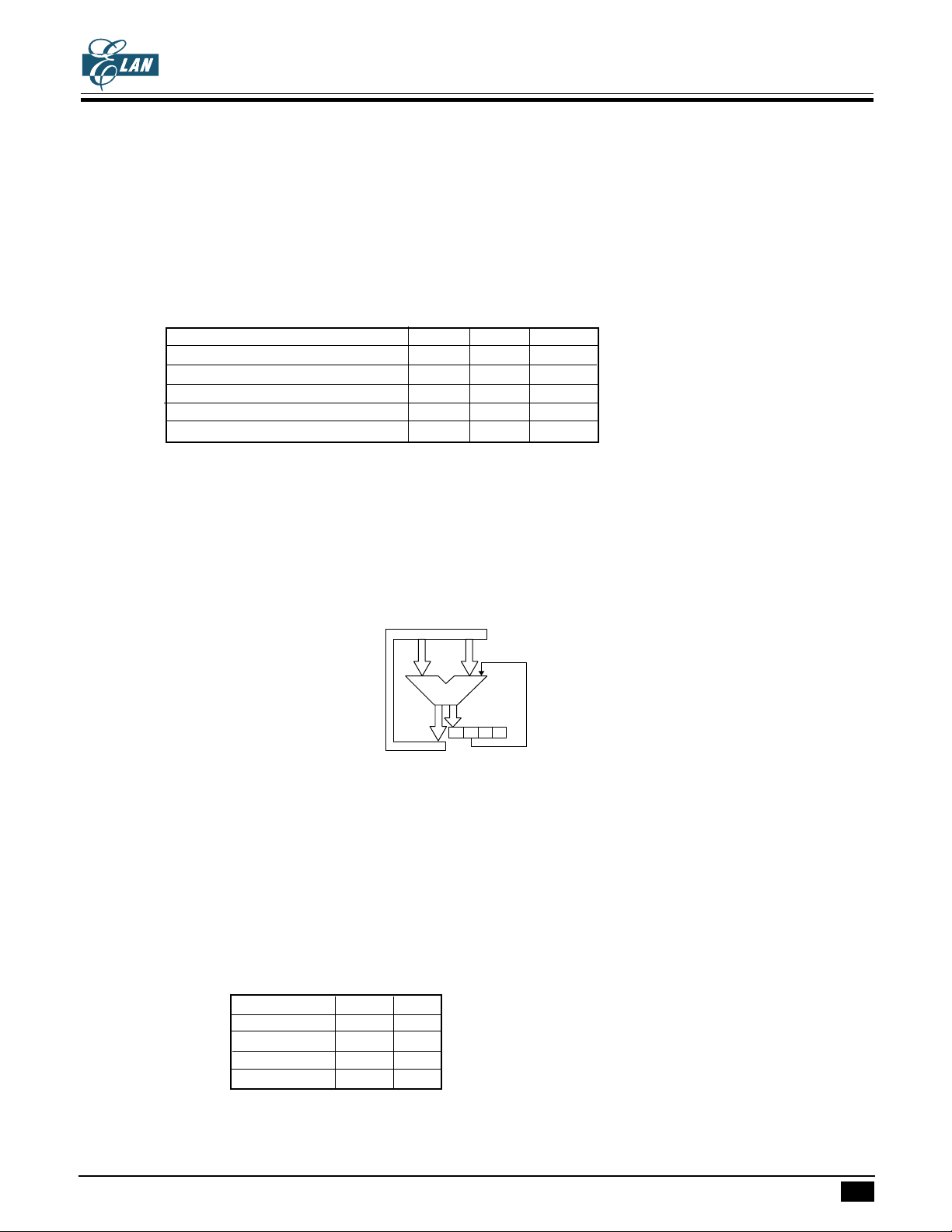
PROGRAM EXAMPLE: Read out the ROM code of address 777h by table-look-up instruction.
LDIA #07h;
STADPL ; [DP]L ← 07h
STADPM ; [DP]M ← 07h
STADPH ; [DP]H ← 07h, Load DP=777h
:
LDL #00h;
LDH #03h;
LDAX ; ACC ← 6h
STAMI ; RAM[30] ← 6h
LDAXI ; ACC ← 5h
STAM ; RAM[31] ← 5h
;
ORG 777h
DATA 56h;
:
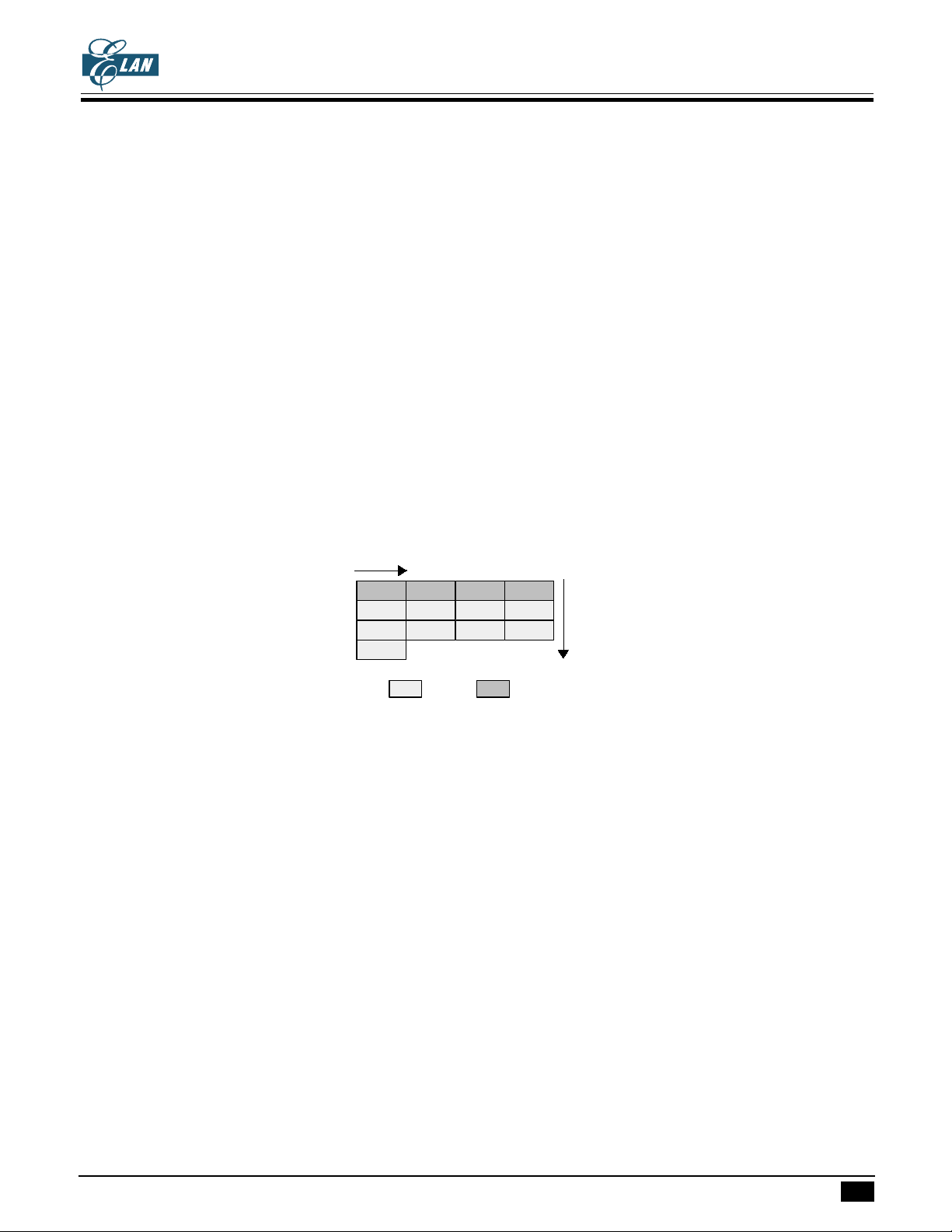
DATA RAM ( 52-nibble ) DATA RAM ( 52-nibble )
DATA RAM ( 52-nibble )
DATA RAM ( 52-nibble ) DATA RAM ( 52-nibble )
EM73P362EM73P362
EM73P362
EM73P362EM73P362
There is total 52 - nibble data RAM from address 00 to 33h
Data RAM includes 3 parts: zero page region, stacks and data area.
Address
00h - 0Fh
10h - 1Fh
20h - 2Fh
30h - 33h
Increment
Level 0
Level 4
Level 8
Level 12
Level 1
Level 5
Level 9
Level 2
Level 6
Level 10
Stack Zero-page
Level 3
Level 7
Level 11
Increment
ZERO- PAGE:
From 00h to 0Fh is the location of zero-page. It is used as the pointer in zero-page addressing mode for the
instruction of "STD #k,y; ADD #k,y; CLR y,b; CMP k,y".
PROGRAM EXAMPLE: To wirte immediate data "07h" to address "03h" of RAM and to clear bit 2 of RAM.
STD #07h, 03h ; RAM[03] ← 07h
CLR 0Eh,2 ; RAM[0Eh]2 ← 0
STACK:
There are 13-level (maximum) stack for user using for subroutine (including interrupt and CALL). User can
assign any level be the starting stack by giving the level number to stack pointer (SP).
When user using any instruction of CALL or subroutine, before entry the subroutine, the previous PC address
will be saved into stack until return from those subroutines, the PC value will be restored by the data saved
in stack.
DATA AREA:
Except the special area used by user, the whole RAM can be used as data area for storing and loading general
data.
*
This specification are subject to be changed without notice.
11.1.2001
6
EM73P362EM73P362
EM73P362
EM73P362EM73P362
4-BIT MICRO-CONTROLLER FOR LCD PRODUCT4-BIT MICRO-CONTROLLER FOR LCD PRODUCT
4-BIT MICRO-CONTROLLER FOR LCD PRODUCT
4-BIT MICRO-CONTROLLER FOR LCD PRODUCT4-BIT MICRO-CONTROLLER FOR LCD PRODUCT
ADDRESSING MODE
(1) Indirect addressing mode:
Indirect addressing mode indicates the RAM address by specified HL register.
For example:
LDAM ; Acc ← RAM[HL]
STAM ; RAM[HL] ← Acc
(2) Direct addressing mode:
Direct addressing mode indicates the RAM address by immediate data.
For example:
LDA x ; Acc← RAM[x]
STA x ; RAM[x] ← Acc
(3) Zero-page addressing mode
For zero-page region, user can using direct addressing to write or do any arithematic, comparsion or bit
manupulated operation directly.
For example: STD #k,y ; RAM[y] ← #k
ADD #k,y; RAM[y] ← RAM[y] + #k
LCD DISPLALCD DISPLA
LCD DISPLA
LCD DISPLALCD DISPLA
Y RAMY RAM
Y RAM
Y RAMY RAM
RAM address from 40h ~ 46h, 50h ~ 56h, 60h ~ 66h are LCD display RAM, the RAM data of this region can't
be operated by instruction “LDHL xx” and “EXHL”.
40h~46h (COM0)
50h~56h (COM1)
60h~66h (COM2)
PROGRAM COUNTER (3K ROM)PROGRAM COUNTER (3K ROM)
PROGRAM COUNTER (3K ROM)
PROGRAM COUNTER (3K ROM)PROGRAM COUNTER (3K ROM)
Address Increment bit 0 1 2 3 0 1 2
SEG0
SEG1
SEG2
SEG3
SEG4
SEG5
SEG6
SEG7
SEG8
SEG9
SEG10
SEG11
SEG12
SEG13
SEG14
SEG15
SEG16
SEG17
SEG18
SEG19
SEG20
SEG21
SEG22
SEG23
SEG24
SEG25
SEG26
Increment
Program counter ( PC ) is composed by a 12-bit counter, which indicates the next executed address for the
instruction of program ROM.
For a 3K - byte size ROM, PC can indicate address form 000h - BFFh, for BRANCH and CALL instructions,
PC is changed by instruction indicating.
(1) Branch instruction:(1) Branch instruction:
(1) Branch instruction:
(1) Branch instruction:(1) Branch instruction:
SBR aSBR a
SBR a
SBR aSBR a
Object code: 00aa aaaa
Condition: SF=1; PC ← PC
( branch condition satisified )
11-6.a
PC Hold original PC value+1 aaaaaa
SF=0; PC← PC +1( branch condition not satisified)
PC Original PC value + 1
LBR aLBR a
LBR a
LBR aLBR a
Object code: 1100 aaaa aaaa aaaa
Condition: SF=1; PC ← a ( branch condition satisified)
PCaaaaaaaaaaaa
*
This specification are subject to be changed without notice.
11.1.2001
7
4-BIT MICRO-CONTROLLER FOR LCD PRODUCT4-BIT MICRO-CONTROLLER FOR LCD PRODUCT
4-BIT MICRO-CONTROLLER FOR LCD PRODUCT
4-BIT MICRO-CONTROLLER FOR LCD PRODUCT4-BIT MICRO-CONTROLLER FOR LCD PRODUCT
SF=0 ; PC ← PC + 2 (branch condition not satisfied)
PC Original PC value + 2
(2) Subroutine instruction:(2) Subroutine instruction:
(2) Subroutine instruction:
(2) Subroutine instruction:(2) Subroutine instruction:
SCALL aSCALL a
SCALL a
SCALL aSCALL a
Object code: 1110 nnnn
Condition : PC ← a ; a=8n+6 ; n=1..15 ; a=86h, n=0
PC 0 0 0 0 a a a a a a a a
LCALL aLCALL a
LCALL a
LCALL aLCALL a
Object code: 0100 0aaa aaaa aaaa
Condition: PC ← a
PC0aaaaaaaaaaa
EM73P362EM73P362
EM73P362
EM73P362EM73P362
RETRET
RET
RETRET
Object code: 0100 1111
Condition: PC ← STACK[SP]; SP + 1
PC The return address stored in stack
RT IRT I
RT I
RT IRT I
Object code: 0100 1101
Condition : FLAG. PC ← STACK[SP]; EI ← 1; SP + 1
PC The return address stored in stack
(3) Interrupt acceptance operation:(3) Interrupt acceptance operation:
(3) Interrupt acceptance operation:
(3) Interrupt acceptance operation:(3) Interrupt acceptance operation:
When an interrupt is accepted, the original PC is pushed into stack and interrupt vector will be loaded into
PC. The interrupt vectors are as following:
INT0 INT0
INT0 (External interrupt from P0.2)
INT0 INT0
PC000000000010
TRGATRGA
TRGA (Timer A overflow interrupt)
TRGATRGA
PC000000000110
TRGBTRGB
TRGB (Time B overflow interrupt)
TRGBTRGB
PC000000001000
TBITBI
TBI (Time base interrupt)
TBITBI
PC000000001010
*
This specification are subject to be changed without notice.
11.1.2001
8
EM73P362EM73P362
EM73P362
EM73P362EM73P362
4-BIT MICRO-CONTROLLER FOR LCD PRODUCT4-BIT MICRO-CONTROLLER FOR LCD PRODUCT
4-BIT MICRO-CONTROLLER FOR LCD PRODUCT
4-BIT MICRO-CONTROLLER FOR LCD PRODUCT4-BIT MICRO-CONTROLLER FOR LCD PRODUCT
INT1 INT1
INT1 (External interrupt from P0.0)
INT1 INT1
PC000000001100
(4) Reset operation:(4) Reset operation:
(4) Reset operation:
(4) Reset operation:(4) Reset operation:
PC000000000000
(5) Other operations:(5) Other operations:
(5) Other operations:
(5) Other operations:(5) Other operations:
For 1-byte instruction execution: PC + 1
For 2-byte instruction execution: PC + 2
ACCUMULATORACCUMULATOR
ACCUMULATOR
ACCUMULATORACCUMULATOR
Accumulator is a 4-bit data register for temporary data. For the arithematic, logic and comparative opertion
.., ACC plays a role which holds the source data and result.
FLAGSFLAGS
FLAGS
FLAGSFLAGS
There are four kinds of flag, CF (Carry flag), ZF (Zero flag), SF (Status flag) and GF (General flag),
these 4 1-bit flags are affected by the arithematic, logic and comparative .... operation.
All flags will be put into stack when an interrupt subroutine is served, and the flags will be restored after
RTI instruction executed.
(1) Carry Flag ( CF )
The carry flag is affected by following operation :
a. Addition : CF as a carry out indicator, when the addition operation has a carry-out, CF will be "1",
in another word, if the operation has no carry-out, CF will be "0".
b. Subtraction : CF as a borrow-in indicator, when the subtraction operation must has a borrow, in the CF
will be "0", in another word, if no borrow-in, CF will be "1".
c. Comparision: CF is as a borrow-in indicator for Comparision operation as the same as subtraction
operation.
d. Rotation: CF shifts into the empty bit of accumulator for the rotation and holds the shift out data after
rotation.
e. CF test instruction : For TFCFC instruction, the content of CF sends into SF then clear itself "0".
For TTSFC instruction, the content of CF sends into SF then set itself "1".
(2) Zero Flag ( ZF )
ZF is affected by the result of ALU, if the ALU operation generate a "0" result, the ZF will be "1",
otherwise, the ZF will be "0".
(3) Status Flag ( SF )
The SF is affected by instruction operation and system status.
*
This specification are subject to be changed without notice.
11.1.2001
9
4-BIT MICRO-CONTROLLER FOR LCD PRODUCT4-BIT MICRO-CONTROLLER FOR LCD PRODUCT
4-BIT MICRO-CONTROLLER FOR LCD PRODUCT
4-BIT MICRO-CONTROLLER FOR LCD PRODUCT4-BIT MICRO-CONTROLLER FOR LCD PRODUCT
a. SF is initiated to "1" for reset condition.
b. Branch instruction is decided by SF, when SF=1, branch condition will be satisified, otherwise,
branch condition will not be satisified by SF = 0.
(4) General Flag ( GF )
GF is a one bit general purpose register which can be set, clear, test by instruction SGF, CGF and TGS.
PROGRAM EXAMPLE :
Check following arithematic operation for CF, ZF, SF
CF Z F SF
LDIA #00h; - 1 1
LDIA #03h; - 0 1
ADDA #05h; - 0 1
ADDA #0Dh; - 0 0
ADDA #0Eh; - 0 0
ALUALU
ALU
ALUALU
EM73P362EM73P362
EM73P362
EM73P362EM73P362
The arithematic operation of 4 - bit data is performed in ALU unit. There are 2 flags can be affected by
the result of ALU operation, ZF and SF. The operation of ALU can be affected by CF only.
ALU STRUCTUREALU STRUCTURE
ALU STRUCTURE
ALU STRUCTUREALU STRUCTURE
ALU supported user arithematic operation function, including : addition, subtraction and rotaion.
DATA BUS
ALU
ZF CF SF GF
ALU FUNCTIONALU FUNCTION
ALU FUNCTION
ALU FUNCTIONALU FUNCTION
(1) Addition:
For instruction ADDAM, ADCAM, ADDM #k, ADD #k,y .... ALU supports addition function.
The addition operation can affect CF and ZF. For addition operation, if the result is "0", ZF will be "1",
otherwise, not equal "0", ZF will be "0". When the addition operation has a carry-out, CF will be "1",
otherwise, CF will be "0".
EXAMPLE:
Operation Carry Zero
3+4=7 0 0
7+F=6 1 0
0+0=0 0 1
8+8=0 1 1
(2) Subtraction:
For instruction SUBM #k, SUBA #k, SBCAM, DECM... ALU supports user subtraction function. The
subtraction operation can affect CF and ZF, For subtraction operation, if the result is negative, CF will
*
This specification are subject to be changed without notice.
11.1.2001
10
EM73P362EM73P362
EM73P362
EM73P362EM73P362
4-BIT MICRO-CONTROLLER FOR LCD PRODUCT4-BIT MICRO-CONTROLLER FOR LCD PRODUCT
4-BIT MICRO-CONTROLLER FOR LCD PRODUCT
4-BIT MICRO-CONTROLLER FOR LCD PRODUCT4-BIT MICRO-CONTROLLER FOR LCD PRODUCT
be "0", it means a borrow out, otherwise, if the result is positive, CF will be "1". For ZF, if the result
of subtraction operation is "0", the ZF will be "1", otherwise, ZF will be "1".
EXAMPLE:
Operation Carry Zero
8-4=4 1 0
7-F= -8(1000) 0 0
9-9=0 1 1
(3) Rotation:
There are two kinds of rotation operation, one is rotation left, the other is rotation right.
RLCA instruction rotates Acc value to left, shift the CF value into the LSB bit of Acc and the shift out data
will be hold in CF.
MSB LSB
ACC
CF
RRCA instruction operation rotates Acc value to right, shift the CF value into the MSB bit of Acc and
the shift out data will be hold in CF.
MSB LSB
ACC
CF
PROGRAM EXAMPLE: To rotate Acc right and shift a "1" into the MSB bit of Acc.
TTCFS; CF ← 1
RRCA; rotate Acc right and shift CF=1 into MSB.
HL REGISTERHL REGISTER
HL REGISTER
HL REGISTERHL REGISTER
HL register are two 4-bit registers, they are used as a pair of pointer for the address of RAM memory and also
2 independent temporary 4-bit data registers. For some instruction, L register can be a pointer to indicate the
pin number (Port4, Port6, Port7).
HL REGISTER STRUCTUREHL REGISTER STRUCTURE
HL REGISTER STRUCTURE
HL REGISTER STRUCTUREHL REGISTER STRUCTURE
HL REGISTER FUNCTIONHL REGISTER FUNCTION
HL REGISTER FUNCTION
HL REGISTER FUNCTIONHL REGISTER FUNCTION
3 2 1 0
H REGISTER
3 2 1 0
L REGISTER
(1)For instruction : LDL #k, LDH #k, THA, THL, INCL, DECL, EXAL, EXAH, HL register used as a
temporary register.
PROGRAM EXAMPLE: Load immediate data "5h" into L register, "Dh" into H register.
LDL #05h;
LDH #0Dh;
(2) For instruction LDAM, STAM, STAMI .., HL register used as a pointer for the address of RAM memory.
*
This specification are subject to be changed without notice.
11.1.2001
11
EM73P362EM73P362
EM73P362
EM73P362EM73P362
4-BIT MICRO-CONTROLLER FOR LCD PRODUCT4-BIT MICRO-CONTROLLER FOR LCD PRODUCT
4-BIT MICRO-CONTROLLER FOR LCD PRODUCT
4-BIT MICRO-CONTROLLER FOR LCD PRODUCT4-BIT MICRO-CONTROLLER FOR LCD PRODUCT
PROGRAM EXAMPLE: Store immediate data #Ah into RAM of address 35h.
LDL #5h;
LDH #3h;
STDMI #0Ah; RAM[35] ← Ah
(3) For instruction : SELP, CLPL, TFPL, L register be a pointer to indicate the bit of I/O port.
When LR = 0 - 1, indicate P4.0 - P4.1.
PROGRAM EXAMPLE: To set bit 1 of Port 4 to "1"
LDL #01h;
SEPL ; P4.1 ← 1
STACK POINTER (SP)STACK POINTER (SP)
STACK POINTER (SP)
STACK POINTER (SP)STACK POINTER (SP)
Stack pointer is a 4-bit register which stores the present stack level number.
Before using stack, user must set the SP value first, CPU will not initiate the SP value after reset condition.
When a new subroutine is accepted, the SP will be decreased one automatically, in another word, if
returning from a subroutine, the SP will be increased one.
The data transfer between ACC and SP is by instruction of "LDASP" and "STASP".
DATA POINTER (DP)DATA POINTER (DP)
DATA POINTER (DP)
DATA POINTER (DP)DATA POINTER (DP)
Data pointer is a 12-bit register which stores the address of ROM can indicate the ROM code data
specified by user (refer to data ROM).
CLOCK AND TIMING GENERATORCLOCK AND TIMING GENERATOR
CLOCK AND TIMING GENERATOR
CLOCK AND TIMING GENERATORCLOCK AND TIMING GENERATOR
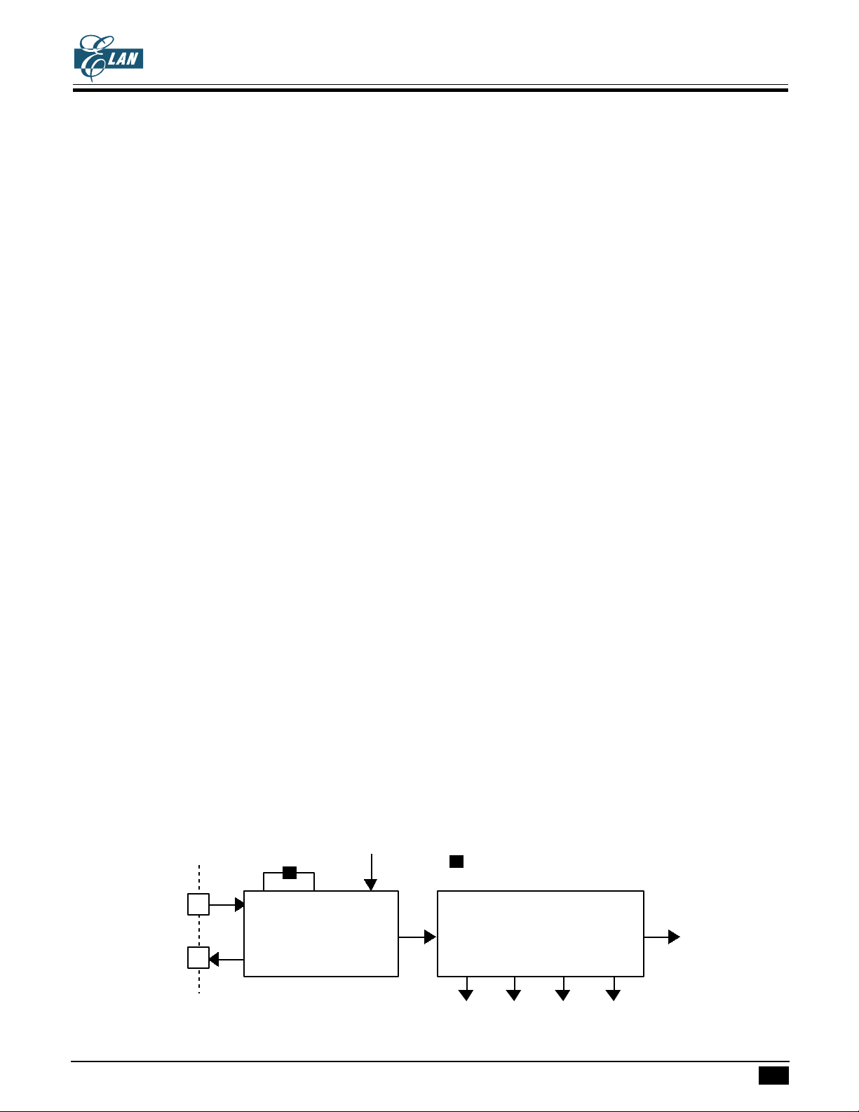
The clock generator is supported by a single clock system, the clock source comes from crystal (resonator)
or RC oscillation, the working frequency range is 32 KHz to 100 KHz depending on the working voltage.
CLOCK AND TIMING GENERATOR STRUCTURECLOCK AND TIMING GENERATOR STRUCTURE
CLOCK AND TIMING GENERATOR STRUCTURE
CLOCK AND TIMING GENERATOR STRUCTURECLOCK AND TIMING GENERATOR STRUCTURE
The clock generator connects outside compoments (crystal or resonator by XIN and XOUT pin for crystal
osc type, capacitor for RC osc type, these two type is decided by mask option) the clock generator
generates a basic system clock "fc".
When CPU sleeping, the clock generator will be stopped until the sleep condition released.
The system clock control generates 4 basic phase signals (S1, S2, S3, S4) and system clock.
Mask option
XIN
sleep
fc
Mask option for choose Crystal or RC oscillation
System clock
clock generator System clock control
XOUT
*
This specification are subject to be changed without notice.
S1 S2 S3 S4
11.1.2001
12
EM73P362EM73P362
EM73P362
EM73P362EM73P362
4-BIT MICRO-CONTROLLER FOR LCD PRODUCT4-BIT MICRO-CONTROLLER FOR LCD PRODUCT
4-BIT MICRO-CONTROLLER FOR LCD PRODUCT
4-BIT MICRO-CONTROLLER FOR LCD PRODUCT4-BIT MICRO-CONTROLLER FOR LCD PRODUCT
XIN
XOUT
Crystal connection
CLOCK AND TIMING GENERATOR FUNCTIONCLOCK AND TIMING GENERATOR FUNCTION
CLOCK AND TIMING GENERATOR FUNCTION
CLOCK AND TIMING GENERATOR FUNCTIONCLOCK AND TIMING GENERATOR FUNCTION
Resistor connection
XIN
XOUT
The frequency of fc is the oscillation frequency for XIN, XOUT by crystal (resonator) or by RC osc.
When CPU sleeps, the XOUT pin will be in "high" state.
The instruction cycle equal 4 basic clock fc.
1 instructure cycle = 4 / fc
OPERATION MODE CONTROLOPERATION MODE CONTROL
OPERATION MODE CONTROL
OPERATION MODE CONTROLOPERATION MODE CONTROL
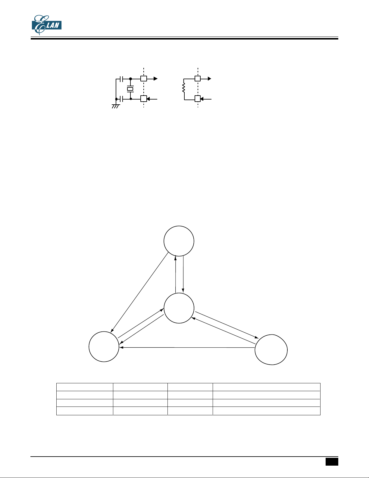
EM73P362 has 3 operation modes. They are Normal, Idle, and Stop mode.
IDLE
mode
(P19)
Reset
Reset release
Reset
RESET
operation
Command
NORMAL
operating
mode
Reset
Input pin or
Internal timer wakeup
Input timer wakeup
Command
(P16)
STOP
mode
Operation Mode Oscillator CPU Available Function
Normal Oscillating Run LCD, RFC, Low battery detector
Idle Oscillating Run LCD
Stop Stop Stop All disable
*
This specification are subject to be changed without notice.
11.1.2001
13
EM73P362EM73P362
EM73P362
EM73P362EM73P362
4-BIT MICRO-CONTROLLER FOR LCD PRODUCT4-BIT MICRO-CONTROLLER FOR LCD PRODUCT
4-BIT MICRO-CONTROLLER FOR LCD PRODUCT
4-BIT MICRO-CONTROLLER FOR LCD PRODUCT4-BIT MICRO-CONTROLLER FOR LCD PRODUCT
ST ST
ST
ST ST
During STOP operation mode, CPU holds the system’s internal status with a low power consumption, for
the STOP mode, the system clock will be stopped in the STOP condition and system need a warm up time
for the stability of system clock running after wakeup.
The STOP operation mode is controlled by Port 16 and released by P0(0..3)/
P16 3 2 1 0 Initial value : 0000
STOP operation mode condition :
1. Osc stop and CPU internal status held.
2. Internal time base clear to "0".
3. CPU internal memory, flags, register, I/O held original states.
4. Program counter hold the executed address after STOP release.
Release condition :
1. Release STOP operation mode by the falling edge of any one of P0(0..3)/
2. Osc start to oscillating.
3. Warm-up time passing.
4. According PC to execute the following program.
OP OPERAOP OPERA
OP OPERA
OP OPERAOP OPERA
TION MODETION MODE
TION MODE
TION MODETION MODE
WAKEUP 0 3..
SPME SWWT
SPME Enable STOP mode SWWT Set wake-up warm-up time
9
0 1 Enable STOP mode 0 0 2
* * Reserved 0 1 2
1 0 2
/ XIN
14
/ XIN
16
/ XIN
1 1 Reserved
WAKEUP 0 3..
.
.
Note : There are 4 independent mask options for wakeup function in EM73P362. So, the wakeup function
of P0(0..3)/
IDLE OPERAIDLE OPERA
IDLE OPERA
IDLE OPERAIDLE OPERA
The IDLE operation mode retains the internal status with low power consumption without stopping the
system clock function and LCD display.
The IDLE operation mode is controlled by Port 19 and released by P0(0..3)/
timing generator.
P19 3 2 1 0 Initial value : 0000
IDME SIDR
IDME Enable IDLE mode SIDR Select IDLE releasing condition
0 1 Enable IDLE mode 0 0 P0(0..3) pin input
* * Reserved 0 1 P0(0..3) pin input and 1 sec signal
WAKEUP 0 3..
TION MODETION MODE
TION MODE
TION MODETION MODE
are enabled or disabled independently.
1 0 P0(0..3) pin input and 0.5 sec signal
1 1 P0(0..3) pin input and 15.625m sec signal
WAKEUP 0..3
or the internal
*
This specification are subject to be changed without notice.
11.1.2001
14
 Loading...