

ELAN EM73880 Datasheet

GENERAL DESCRIPTIONGENERAL DESCRIPTION
GENERAL DESCRIPTION
GENERAL DESCRIPTIONGENERAL DESCRIPTION
EM73880 is an advanced single chip CMOS 4-bit micro-controller. It contains 8K-byte ROM, 244-nibble RAM,
4-bit ALU, 13-level subroutine nesting, 22-stage time base, two 12-bit timer/counters for the kernel function.
EM73880 also contains 6 interrupt sources, 1 input port, 2 bidirection ports, LCD display (32x4), and one high
speed timer/counter,sound generator, and speech synthesizer.
EM73880 has plentiful operating modes (SLOW, IDLE, STOP) intended to reduce the power consumption.
FEATURESFEATURES
FEATURES
FEATURESFEATURES
• Operation voltage : 2.4V to 3.6V.
• Clock source : Dual clock system. Low-frequency oscillator (32.768 KHz) could be Crystal or RC
oscillator high-frequency oscillator is a built-in for 4.6 MHz.
• Instruction set : 107 powerful instructions.
• Instruction cycle time : 1.7us for 4.6 MHz (high speed clock).
244 µs for 32768 Hz (low speed clock).
• ROM capacity : 8192 X 8 bits.
• RAM capacity : 244 X 4 bits.
• Input port : 1 port (P0). P0(0..3) and IDLE releasing function are available by mask option.
• Bidirection port : 2 ports (P4, P8). P4.1 is shared with HTC external input. P8(0..3) and IDLE releasing
function are available by mask option.
• 12-bit timer/counter : Two 12-bit timer/counters are programmable for timer, event counter and pulse width
measurement.
• High speed timer/counter : One 8-bit high speed timer/counters is programmable for auto load timer, melody
output and pulse width measurement.
• Speech synthesizer : 160K Speech ROM.
• Built-in time base counter : 22 stages.
• Subroutine nesting : Up to 13 levels.
• Interrupt : External . . . . . 1 input interrupt sources.
Internal . . . . . . 2 Timer overflow interrupts, 1 time base interrupt.
• LCD driver : 32 X 4 dots, 1/4,1/3,1/2, static 4 kinds of duty Type selectable, 1/2 bias, 1/3 bias, 2 kinds
bias Type selectable.
• Power saving function : SLOW, IDLE, STOP operation mode.
• Package type : Chip form. . . . .63 pins.
EM73880EM73880
EM73880
EM73880EM73880
4-BIT MICRO-CONTROLLER FOR LCD PRODUCT4-BIT MICRO-CONTROLLER FOR LCD PRODUCT
4-BIT MICRO-CONTROLLER FOR LCD PRODUCT
4-BIT MICRO-CONTROLLER FOR LCD PRODUCT4-BIT MICRO-CONTROLLER FOR LCD PRODUCT
PreliminaryPreliminary
Preliminary
PreliminaryPreliminary
1 high speed timer/counter overflow interrupt.
1 Speech ending interrupt.
APPLICATIONSAPPLICATIONS
APPLICATIONS
APPLICATIONSAPPLICATIONS
EM73880 is suitable for application in family applicance, consumer products, hand held games and the toy
controller.
* This specification are subject to be changed without notice.
11.30.2001
1
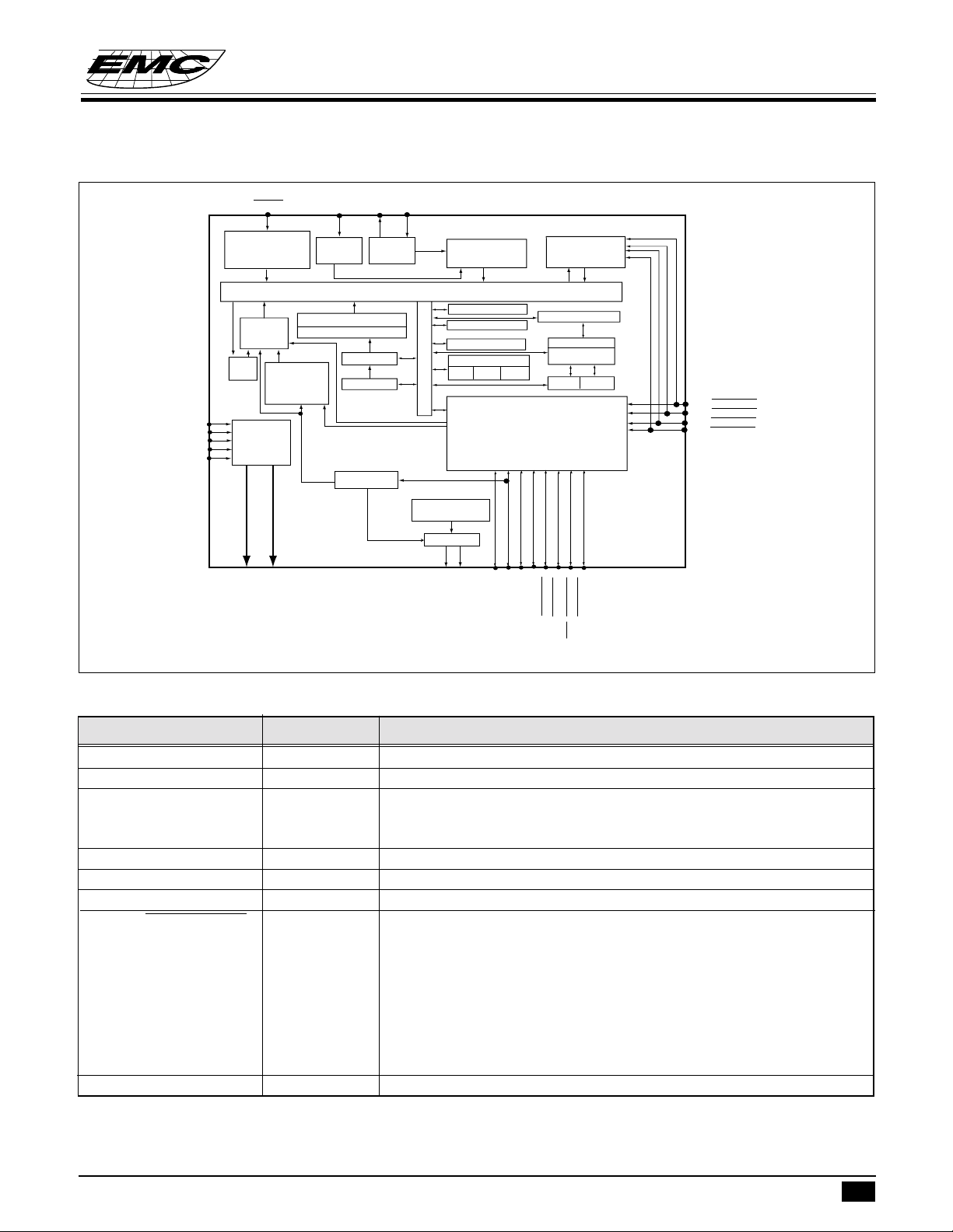
FUNCTION BLOCK DIAGRAMFUNCTION BLOCK DIAGRAM
FUNCTION BLOCK DIAGRAM
FUNCTION BLOCK DIAGRAMFUNCTION BLOCK DIAGRAM
EM73880EM73880
EM73880
EM73880EM73880
4-BIT MICRO-CONTROLLER FOR LCD PRODUCT4-BIT MICRO-CONTROLLER FOR LCD PRODUCT
4-BIT MICRO-CONTROLLER FOR LCD PRODUCT
4-BIT MICRO-CONTROLLER FOR LCD PRODUCT4-BIT MICRO-CONTROLLER FOR LCD PRODUCT
PreliminaryPreliminary
Preliminary
PreliminaryPreliminary
RESET
Reset
Control
Interrupt
Control
Time
Base
Timer/Counter
(TA,TB)
VA
VB
V1
V2
V3
LCD
SEG0~SEG31
COM0~COM3
CLK
LXOUT
Int. Clock
Generator
Instruction Decoder
Instruction Register
ROM
PC
HTC
Clock
Generator
(slow)
LXIN
System Control
Data Bus
Speech Synthesizer
PWM
Z
BZ1
Timing
Generator
Data pointer
ACC
ALU
Flag
C
BZ2
S
I/O Control
P4.0
P4.1/TRGH
Clock Mode
Stack pointer
Stack
HR
P4.2
P4.3
P8.0/WAKEUPA
P8.1(TRGB)/WAKEUPB
Control
RAM
LR
P8.2(INT0)/WAKEUPC
P8.3(TRGA)/WAKEUPD
P0.0/WAKEUP0
P0.1/WAKEUP1
P0.2/WAKEUP2
P0.3/WAKEUP3
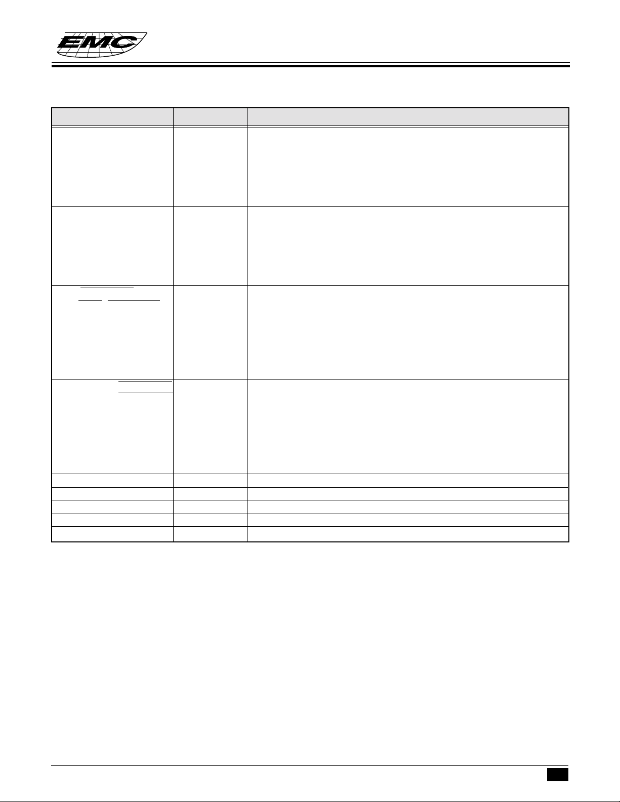
PIN DESCRIPTIONSPIN DESCRIPTIONS
PIN DESCRIPTIONS
PIN DESCRIPTIONSPIN DESCRIPTIONS
SymbolSymbol
Symbol
SymbolSymbol
V
DD, VDD2
V
SS
Pin-typePin-type
Pin-type
Pin-typePin-type
FunctionFunction
Function
FunctionFunction
Power supply (+) / speech synthesizer power supply(+)
Power supply (-)
RESET RESET-A System reset input signal, low active
mask option : none
pull-up
CLK OSC-G Capacitor connecting pin for internal high frequency OSC.
LXIN OSC-B/OSC-H Crstal/RC connecting pin for low speed clock source
LXOUT OSC-B Crstal/RC connecting pin for low speed clock source
P0(0..3)/WAKEUP0..3 INPUT-K 4-bit input port with IDLE releasing function
mask option : wakeup enable, negative edge release, pull-up
wakeup enable, negative edge release, none
wakeup enable, positive edge release, pull-down
wakeup enable, positive edge release, none
wakeup disable, pull-up
wakeup disable, pull-down
wakeup disable, none
P4.0 I/O-R 1-bit bidirection I/O port
* This specification are subject to be changed without notice.
11.30.2001
2
EM73880EM73880
EM73880
EM73880EM73880
4-BIT MICRO-CONTROLLER FOR LCD PRODUCT4-BIT MICRO-CONTROLLER FOR LCD PRODUCT
4-BIT MICRO-CONTROLLER FOR LCD PRODUCT
4-BIT MICRO-CONTROLLER FOR LCD PRODUCT4-BIT MICRO-CONTROLLER FOR LCD PRODUCT
PreliminaryPreliminary
Preliminary
PreliminaryPreliminary
PIN DESCRIPTIONSPIN DESCRIPTIONS
PIN DESCRIPTIONS
PIN DESCRIPTIONSPIN DESCRIPTIONS
SymbolSymbol
Symbol
SymbolSymbol
P4.1/TRGH I/O-Q 1-bit bidirection I/O port with HTC external input
P4(2,3) I/O-Q 2-bit bidirection I/O port with high current source
P8.0/WAKEUPA, I/O-S 2-bit bidirection I/O port with external interrupt source input only
P8.2/INT0/WAKEUPC P8.2 and IDLE releasing function
P8.1(TRGB)/WAKEUPB I/O-S 2-bit bidirection I/O port with time/counter A,B external input and IDLE
P8.3(TRGA)/WAKEUPD releasing function
BZ1, BZ2 Speech output pin
VA,VB, V1, V2, V3 Connect the capacitors for LCD bias voltage
COM0~COM3 LCD common output pins
SEG0~SEG31 LCD segment output pins
TEST Tie Vss as package type, no connecting as COB type
Pin-typePin-type
Pin-type
Pin-typePin-type
FunctionFunction
Function
FunctionFunction
mask option : NMOS open-drain
PMOS open-drain
low current push-pull
normal current push-pull
high current push-pull
mask option : NMOS open-drain
PMOS open-drain
low current push-pull
normal current push-pull
high current push-pull
mask option : wakeup enable, low current push-pull
wakeup enable, normal current push-pull
wakeup disable, open-drain
wakeup disable, low current push-pull
wakeup disable, normal current push-pull
mask option : wakeup enable, low current push-pull
wakeup enable, normal current push-pull
wakeup disable, open-drain
wakeup disable, low current push-pull
wakeup disable, normal current push-pull
FUNCTION DESCRIPTIONSFUNCTION DESCRIPTIONS
FUNCTION DESCRIPTIONS
FUNCTION DESCRIPTIONSFUNCTION DESCRIPTIONS
PROGRAM ROM (8K X 8 bits)PROGRAM ROM (8K X 8 bits)
PROGRAM ROM (8K X 8 bits)
PROGRAM ROM (8K X 8 bits)PROGRAM ROM (8K X 8 bits)
8 K x 8 bits program ROM contains user's program and some fixed data.
The basic structure of program ROM can be divided into 6 parts.
1. Address 000h: Reset start address.
2. Address 002h - 00Ch : 6 kinds of interrupt service routine entry addresses.
3. Address 00Eh-086h : SCALL subroutine entry address, only available at 00Eh,016h,01Eh,026h, 02Eh,
036h, 03Eh, 046h, 04Eh, 056h, 05Eh, 066h, 06Eh, 076h, 07Eh, 086h.
4. Address 000h - 7FFh : LCALL subroutine entry address
5. Address 000h - 1FFFh :Except used as above function, the other region can be used as user's program region.
6. Address 1000h - 1FFFh : Fixed data stortage area.
* This specification are subject to be changed without notice.
11.30.2001
3
EM73880EM73880
EM73880
EM73880EM73880
4-BIT MICRO-CONTROLLER FOR LCD PRODUCT4-BIT MICRO-CONTROLLER FOR LCD PRODUCT
4-BIT MICRO-CONTROLLER FOR LCD PRODUCT
4-BIT MICRO-CONTROLLER FOR LCD PRODUCT4-BIT MICRO-CONTROLLER FOR LCD PRODUCT
PreliminaryPreliminary
Preliminary
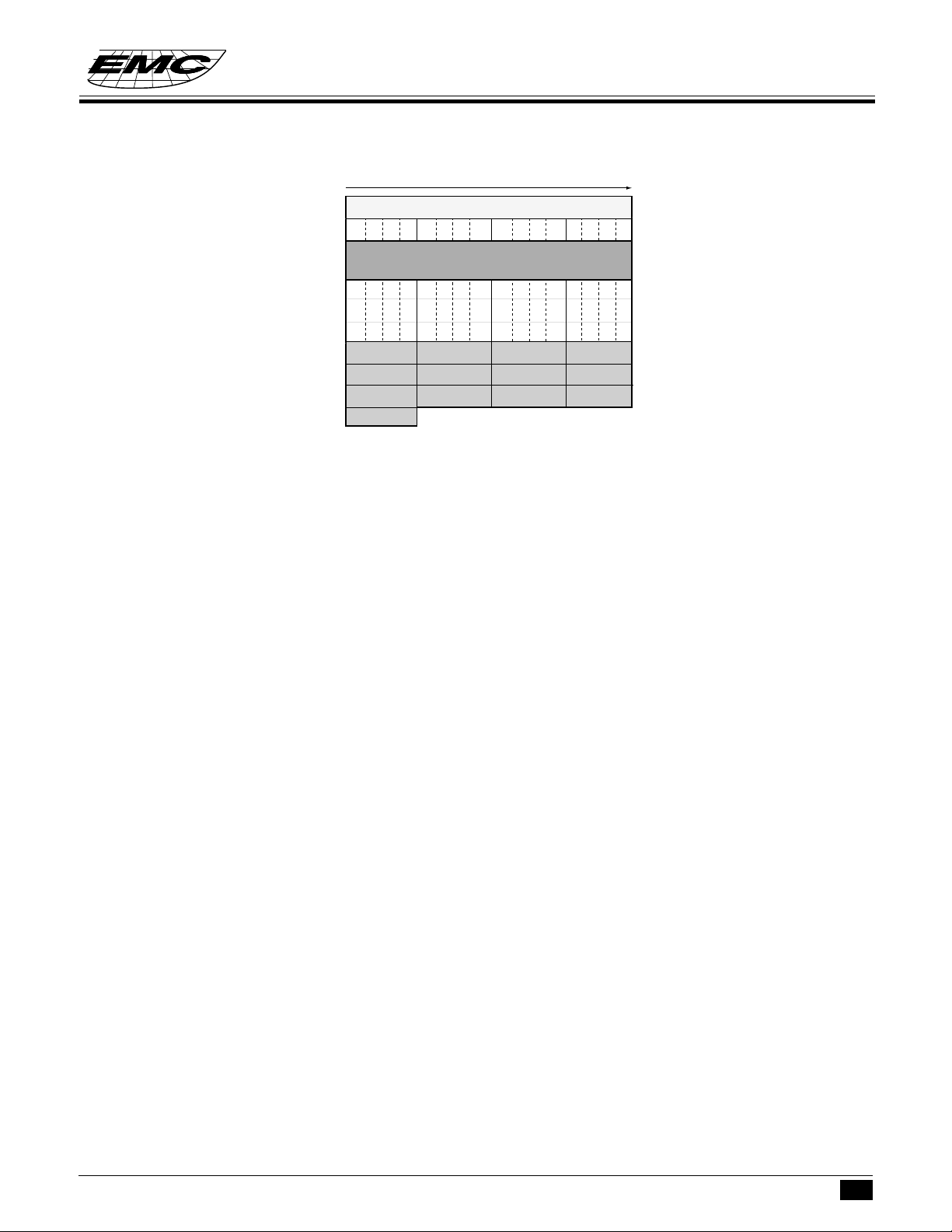
address 8192 x 8 bits
PreliminaryPreliminary
000h Reset start address
002h INT0; External interrupt service routine entry address
004h HTCI; High speed timer interrupt service entry address
006h TRGA; Timer/counterA interrupt service routine entry address LCALL entry
008h TRGB; Timer/counter B interrupt service routine entry address address
00Ah TBI; Time base interrupt service routine entry address
00Ch SPI
00Eh
086h
800h
.
.
.
SCALL, subroutine call entry address
1000
FFFh fixed data area
Bank1
1FFF
User's program and fixed data are stored in the program ROM. User's program is according the PC value
to send next executed instruction code . Fixed data can be read out.
The program counter is a 13-bit binary counter. The PC can defined 8K ROM.
Table -look-up instruction is depended on the Data Pointer (DP) to indicate to ROM address, then to get the
ROM code data. The fixed data only can be put in bank1.
LDAXLDAX
LDAX
LDAXLDAX
LDAXILDAXI
LDAXI
LDAXILDAXI
Acc Acc
Acc
Acc Acc
Acc Acc
Acc
Acc Acc
←←
ROM[DP] ROM[DP]
←
ROM[DP]
←←
ROM[DP] ROM[DP]
←←
ROM[DP] ROM[DP]
←
ROM[DP]
←←
ROM[DP] ROM[DP]
LL
L
LL
,DP+1,DP+1
,DP+1
,DP+1,DP+1
HH
H
HH
DP is a 12-bit data register which can store the program ROM address to be the pointer for the ROM code
data. First, user load ROM address into DP by instruction "STADPL, STADPM, STADPH", then user can
get the lower nibble of ROM code data by instruction "LDAX" and higher nibble by instruction "LDAXI"
PROGRAM EXAMPLE: Read out the ROM code of address 1777h by table-look-up instruction.
LDIA #07h;
STADPL ; DP2-0 ← 07h
STADPM ; DP5-3 ← 07h
STADPH ; DP8-6 ← 07h, Load DP=777h
:
LDL #00h;
LDH #03h;
LDAX ; ACC ← 6h
STAMI ; RAM[30] ← 6h
LDAXI ; ACC ← 5h
STAM ; RAM[31] ← 5h
;
ORG 1777H
DATA 56H;
:
DATA RAM ( 244-nibble ) DATA RAM ( 244-nibble )
DATA RAM ( 244-nibble )
DATA RAM ( 244-nibble ) DATA RAM ( 244-nibble )
There is total 244 - nibble data RAM from address 00 to F3h
Data RAM includes 3 parts: zero page region, stacks and data area.
* This specification are subject to be changed without notice.
11.30.2001
4
EM73880EM73880
EM73880
EM73880EM73880
4-BIT MICRO-CONTROLLER FOR LCD PRODUCT4-BIT MICRO-CONTROLLER FOR LCD PRODUCT
4-BIT MICRO-CONTROLLER FOR LCD PRODUCT
4-BIT MICRO-CONTROLLER FOR LCD PRODUCT4-BIT MICRO-CONTROLLER FOR LCD PRODUCT
PreliminaryPreliminary
Preliminary
PreliminaryPreliminary
Increment
Address
00h~0Fh
10h~1Fh
20h~2Fh
30h~3Fh
40h~4Fh
:
B0h ~ BFh
C0h ~ CFh
D0h ~ DFh
E0h ~ EFh
F0h ~ F3h
level 0
level 4
level 8
level C
zero page
LCD display RAM
level 1
level 5
level 9
level 2
level 6
level A
level 3
level 7
level B
LCD display RAM:
RAM address from 20h ~ 3Fh are the LCD display RAM area, the RAM data of this region can't be operated
by instruction LDHL xx and EXHL.
ZERO- PAGE:
From 00h to 0Fh is the location of zero-page . It is used as the pointer in zero -page addressing mode for the
instruction of "STD #k,y; ADD #k,y; CLR y,b; CMP k,y".
PROGRAM EXAMPLE: To wirte immediate data "07h" to address "03h" of RAM and to clear bit 2 of RAM.
STD #07h, 03h ; RAM[03] ← 07h
CLR 0Eh,2 ; RAM[0Eh]2 ← 0
STACK:
There are 13 - level (maximum) stack for user using for subroutine (including interrupt and CALL). User
can assign any level be the starting stack by giving the level number to stack pointer (SP).
When user using any instruction of CALL or subroutine, before entry the subroutine, the previous PC address
will be saved into stack until return from those subroutines ,the PC value will be restored by the data saved
in stack.
DATA AREA:
Except the special area used by user, the whole RAM can be used as data area for storing and loading general
data.
ADDRESSING MODE
(1) Indirect addressing mode:
Indirect addressing mode indicates the RAM address by specified HL register.
For example: LDAM ; Acc ← RAM[HL]
STAM ; RAM[HL] ← Acc
(2) Direct addressing mode:
Direct addressing mode indicates the RAM address by immediate data.
* This specification are subject to be changed without notice.
11.30.2001
5
EM73880EM73880
EM73880
EM73880EM73880
4-BIT MICRO-CONTROLLER FOR LCD PRODUCT4-BIT MICRO-CONTROLLER FOR LCD PRODUCT
4-BIT MICRO-CONTROLLER FOR LCD PRODUCT
4-BIT MICRO-CONTROLLER FOR LCD PRODUCT4-BIT MICRO-CONTROLLER FOR LCD PRODUCT
PreliminaryPreliminary
Preliminary
For example:
(3) Zero-page addressing mode
For zero-page region, user can using direct addressing to write or do any arithematic, comparsion or bit
manupulated operation directly.
For example:
PROGRAM COUNTER (8K ROM)PROGRAM COUNTER (8K ROM)
PROGRAM COUNTER (8K ROM)
PROGRAM COUNTER (8K ROM)PROGRAM COUNTER (8K ROM)
Program counter ( PC ) is composed by a 13-bit counter, which indicates the next executed address for the
instruction of program ROM.
For a 8K - byte size ROM, PC can indicate address form 0000h - 1FFFh, for BRANCH and CALL instrcutions,
PC is changed by instruction indicating.
(1) Branch instruction:(1) Branch instruction:
(1) Branch instruction:
(1) Branch instruction:(1) Branch instruction:
LDA x ; Acc← RAM[x]
STA x ; RAM[x] ← Acc
STD #k,y ; RAM[y] ← #k
ADD #k,y; RAM[y] ← RAM[y] + #k
PreliminaryPreliminary
SBR aSBR a
SBR a
SBR aSBR a
Object code: 00aa aaaa
Condition: SF=1; PC ← PC
PC Hold original PC value+1 aaaa a a
SF=0; PC← PC +1( branch condition not satisified)
PC Original PC value + 1
LBR aLBR a
LBR a
LBR aLBR a
Object code: 1100 aaaa aaaa aaaa
Condition: SF=1; PC ← a ( branch condition satisified)
PC aaaaaaaaaaa a
SF=0 ; PC ← PC + 2 ( branch condition not satisified )
PC Original PC value + 2
( branch condition satisified )
11-6.a
* This specification are subject to be changed without notice.
11.30.2001
6
4-BIT MICRO-CONTROLLER FOR LCD PRODUCT4-BIT MICRO-CONTROLLER FOR LCD PRODUCT
4-BIT MICRO-CONTROLLER FOR LCD PRODUCT
4-BIT MICRO-CONTROLLER FOR LCD PRODUCT4-BIT MICRO-CONTROLLER FOR LCD PRODUCT
PreliminaryPreliminary
Preliminary
PreliminaryPreliminary
(2) Subroutine instruction:(2) Subroutine instruction:
(2) Subroutine instruction:
(2) Subroutine instruction:(2) Subroutine instruction:
SCALL aSCALL a
SCALL a
SCALL aSCALL a
Object code: 1110 nnnn
Condition : PC ← a ; a=8n+6 ; n=1..15 ; a=86h, n=0
PC0000aaaaaaaa
LCALL aLCALL a
LCALL a
LCALL aLCALL a
Object code: 0100 0 aaa aaaa aaaa
Condition: PC ← a
PC0aaaaaaaaaaa
RETRET
RET
RETRET
Object code: 0100 1111
Condition: PC ← STACK[SP]; SP + 1
EM73880EM73880
EM73880
EM73880EM73880
PC The return address stored in stack
RT IRT I
RT I
RT IRT I
Object code: 0100 1101
Condition : FLAG. PC ← STACK[SP]; EI ← 1; SP + 1
PC The return address stored in stack
* This specification are subject to be changed without notice.
11.30.2001
7
EM73880EM73880
EM73880
EM73880EM73880
4-BIT MICRO-CONTROLLER FOR LCD PRODUCT4-BIT MICRO-CONTROLLER FOR LCD PRODUCT
4-BIT MICRO-CONTROLLER FOR LCD PRODUCT
4-BIT MICRO-CONTROLLER FOR LCD PRODUCT4-BIT MICRO-CONTROLLER FOR LCD PRODUCT
PreliminaryPreliminary
Preliminary
PreliminaryPreliminary
(3) Interrupt acceptance operation:(3) Interrupt acceptance operation:
(3) Interrupt acceptance operation:
(3) Interrupt acceptance operation:(3) Interrupt acceptance operation:
When an interrupt is accepted, the original PC is pushed into stack and interrupt vector will be loaded into
PC,The interrupt vectors are as following:
INT0INT0
INT0 (External interrupt from P8.2)
INT0INT0
PC000000000010
HTCHTC
HTC (High speed counter)
HTCHTC
PC000000000100
TRGATRGA
TRGA (Timer A overflow interrupt)
TRGATRGA
PC000000000110
TRGBTRGB
TRGB (Time B overflow interrupt)
TRGBTRGB
PC000000001000
TBITBI
TBI (Time base interrupt)
TBITBI
PC000000001010
SPISPI
SPI (Speech Interrupt)
SPISPI
PC000000001100
(4) Reset operation:(4) Reset operation:
(4) Reset operation:
(4) Reset operation:(4) Reset operation:
PC000000000000
(5) Other operations:(5) Other operations:
(5) Other operations:
(5) Other operations:(5) Other operations:
For 1-byte instruction execution: PC + 1
For 2-byte instruction execution: PC + 2
For 3-byte instruction execution: PC + 3
ACCUMULATORACCUMULATOR
ACCUMULATOR
ACCUMULATORACCUMULATOR
Accumulator is a 4-bit data register for temporary data . For the arithematic, logic and comparative opertion
.., ACC plays a role which holds the source data and result .
* This specification are subject to be changed without notice.
11.30.2001
8
EM73880EM73880
EM73880
EM73880EM73880
4-BIT MICRO-CONTROLLER FOR LCD PRODUCT4-BIT MICRO-CONTROLLER FOR LCD PRODUCT
4-BIT MICRO-CONTROLLER FOR LCD PRODUCT
4-BIT MICRO-CONTROLLER FOR LCD PRODUCT4-BIT MICRO-CONTROLLER FOR LCD PRODUCT
PreliminaryPreliminary
Preliminary
PreliminaryPreliminary
FLAGSFLAGS
FLAGS
FLAGSFLAGS
There are three kinds of flag, CF ( Carry flag ), ZF ( Zero flag ), SF ( Status flag ), these 3 1-bit flags are affected
by the arithematic, logic and comparative .... operation .
All flags will be put into stack when an interrupt subroutine is served, and the flags will be restored after
RTI instruction executed .
(1) Carry Flag ( CF )
The carry flag is affected by following operation:
a. Addition : CF as a carry out indicator, when the addition operation has a carry-out, CF will be "1",
in another word, if the operation has no carry-out, CF will be "0".
b. Subtraction : CF as a borrow-in indicator, when the subtraction operation must has a borrow, in the CF
will be "0", in another word, if no borrow-in, CF will be "1".
c. Comparision: CF is as a borrow-in indicator for Comparision operation as the same as subtraction
operation.
d. Rotation: CF shifts into the empty bit of accumulator for the rotation and holds the shift out data after
rotation.
e. CF test instruction : For TFCFC instruction, the content of CF sends into SF then clear itself "0".
For TTSFC instruction, the content of CF sends into SF then set itself "1".
(2) Zero Flag ( ZF )
ZF is affected by the result of ALU, if the ALU operation generate a "0" result, the ZF will be "1",
otherwise, the ZF will be "0".
(3) Status Flag ( SF )
The SF is affected by instruction operation and system status .
a. SF is initiated to "1" for reset condition .
b. Branch instruction is decided by SF, when SF=1, branch condition will be satisified, otherwise,
branch condition will not be satisified by SF = 0 .
PROGRAM EXAMPLE:
Check following arithematic operation for CF, ZF, SF
CF ZF SF
LDIA #00h; - 1 1
LDIA #03h; - 0 1
ADDA #05h; - 0 1
ADDA #0Dh; - 0 0
ADDA #0Eh; - 0 0
* This specification are subject to be changed without notice.
11.30.2001
9
EM73880EM73880
EM73880
EM73880EM73880
4-BIT MICRO-CONTROLLER FOR LCD PRODUCT4-BIT MICRO-CONTROLLER FOR LCD PRODUCT
4-BIT MICRO-CONTROLLER FOR LCD PRODUCT
4-BIT MICRO-CONTROLLER FOR LCD PRODUCT4-BIT MICRO-CONTROLLER FOR LCD PRODUCT
PreliminaryPreliminary
Preliminary
PreliminaryPreliminary
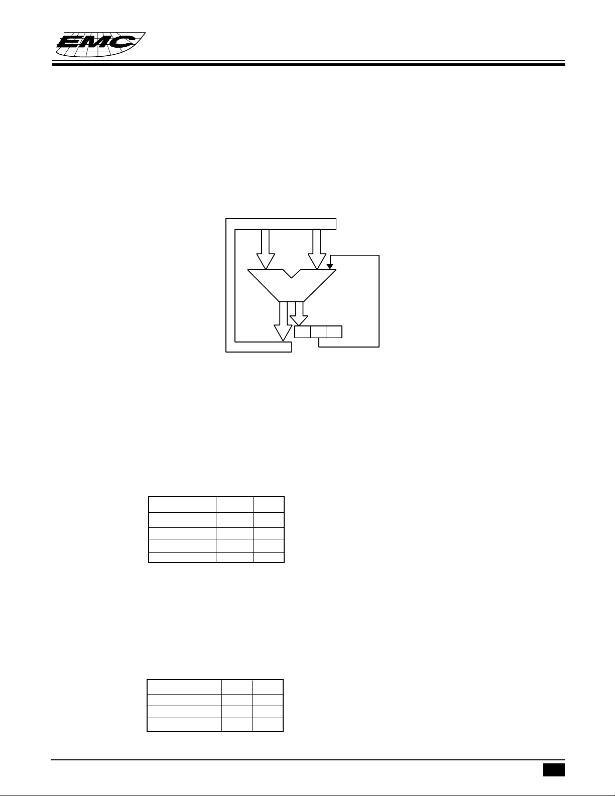
ALUALU
ALU
ALUALU
The arithematic operation of 4 - bit data is performed in ALU unit. There are 2 flags can be affected by the
result of ALU operation, ZF and SF . The operation of ALU can be affected by CF only .
ALU STRUCTUREALU STRUCTURE
ALU STRUCTURE
ALU STRUCTUREALU STRUCTURE
ALU supported user arithematic operation function, including : addition, subtraction and rotaion.
DATA BUS
ALU
ZF CF SF
ALU FUNCTIONALU FUNCTION
ALU FUNCTION
ALU FUNCTIONALU FUNCTION
(1) Addition:
For instruction ADDAM, ADCAM, ADDM #k, ADD #k,y .... ALU supports addition function.
The addition operation can affect CF and ZF. For addition operation, if the result is "0", ZF will be "1",
otherwise, not equal "0", ZF will be "0", When the addition operation has a carry-out. CF will be "1",
otherwise, CF will be "0".
EXAMPLE:
Operation Carry Zero
3+4=7 0 0
7+F=6 1 0
0+0=0 0 1
8+8=0 1 1
(2) Subtraction:
For instruction SUBM #k, SUBA #k, SBCAM, DECM... ALU supports user subtraction function . The
subtraction operation can affect CF and ZF, For subtraction operation, if the result is negative, CF will
be "0", it means a borrow out, otherwise, if the result is positive, CF will be "1". For ZF, if the result
of subtraction operation is "0", the ZF will be "1", otherwise, ZF will be "1".
EXAMPLE:
Operation Carry Zero
8-4=4 1 0
7-F= -8(1000) 0 0
9-9=0 1 1
* This specification are subject to be changed without notice.
11.30.2001
10
EM73880EM73880
3
EM73880
EM73880EM73880
4-BIT MICRO-CONTROLLER FOR LCD PRODUCT4-BIT MICRO-CONTROLLER FOR LCD PRODUCT
4-BIT MICRO-CONTROLLER FOR LCD PRODUCT
4-BIT MICRO-CONTROLLER FOR LCD PRODUCT4-BIT MICRO-CONTROLLER FOR LCD PRODUCT
PreliminaryPreliminary
Preliminary
PreliminaryPreliminary
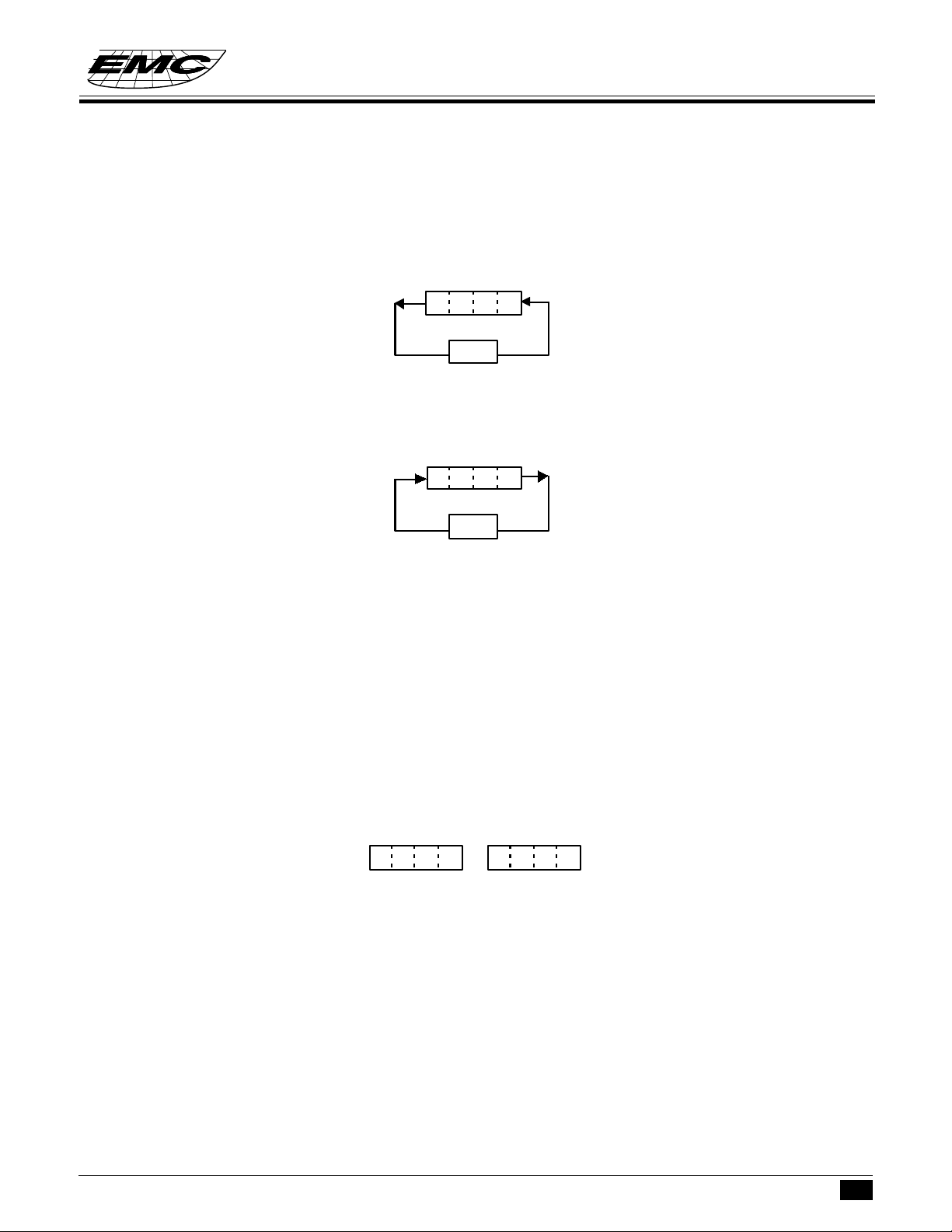
(3) Rotation:
There are two kinds of rotation operation, one is rotation left, the other is rotation right.
RLCA instruction rotates Acc value to left, shift the CF value into the LSB bit of Acc and the shift out data
will be hold in CF.
MSB LSB
ACC
CF
RRCA instruction operation rotates Acc value to right, shift the CF value into the MSB bit of Acc and the
shift out data will be hold in CF.
MSB LSB
ACC
CF
PROGRAM EXAMPLE: To rotate Acc right and shift a "1" into the MSB bit of Acc .
TTCFS; CF ← 1
RRCA; rotate Acc right and shift CF=1 into MSB.
HL REGISTERHL REGISTER
HL REGISTER
HL REGISTERHL REGISTER
HL register are two 4-bit registers, they are used as a pair of pointer for the address of RAM memory and also
2 independent temporary 4-bit data registers. For some instruction, L register can be a pointer to indicate the
pin number ( Port4 ) .
HL REGISTER STRUCTUREHL REGISTER STRUCTURE
HL REGISTER STRUCTURE
HL REGISTER STRUCTUREHL REGISTER STRUCTURE
2 1 0
H REGISTER
3 2 1 0
L REGISTER
* This specification are subject to be changed without notice.
11.30.2001
11

EM73880EM73880
EM73880
EM73880EM73880
4-BIT MICRO-CONTROLLER FOR LCD PRODUCT4-BIT MICRO-CONTROLLER FOR LCD PRODUCT
4-BIT MICRO-CONTROLLER FOR LCD PRODUCT
4-BIT MICRO-CONTROLLER FOR LCD PRODUCT4-BIT MICRO-CONTROLLER FOR LCD PRODUCT
PreliminaryPreliminary
Preliminary
PreliminaryPreliminary
HL REGISTER FUNCTIONHL REGISTER FUNCTION
HL REGISTER FUNCTION
HL REGISTER FUNCTIONHL REGISTER FUNCTION
(1)For instruction : LDL #k, LDH #k, THA, THL, INCL, DECL, EXAL, EXAH, HL register used as a
temporary register .
PROGRAM EXAMPLE:
LDL #05h;
LDH #0Dh;
(2) For instruction LDAM, STAM, STAMI .., HL register used as a pointer for the address of RAM memory.
PROGRAM EXAMPLE: Store immediate data #Ah into RAM of address 35h.
LDL #5h;
LDH #3h;
STDMI #0Ah; RAM[35] ← Ah
(3) For instruction : SELP, CLPL, TFPL, L regieter be a pointer to indicate the bit of I/O port.
When LR = 0 indicate P4.0
PROGRAM EXAMPLE: To set bit 0 of Port4 to "1"
LDL #00h;
SEPL ; P4.0 ← 1
STACK POINTER (SP)STACK POINTER (SP)
STACK POINTER (SP)
STACK POINTER (SP)STACK POINTER (SP)
Stack pointer is a 4-bit register which stores the present stack level number.
Before using stack, user must set the SP value first, CPU will not initiate the SP value after reset condition
. When a new subroutine is accepted, the SP will be decreased one automatically, in another word, if
returning from a subroutine, the SP will be increased one .
The data transfer between ACC and SP is by instruction of "LDASP" and "STASP".
Load immediate data "5h" into L register, "Dh" into H register.
DATA POINTER (DP)DATA POINTER (DP)
DATA POINTER (DP)
DATA POINTER (DP)DATA POINTER (DP)
Data pointer is a 12-bit register which stores the address of ROM can indicate the ROM code data
specified by user (refer to data ROM).
CLOCK AND TIMING GENERATORCLOCK AND TIMING GENERATOR
CLOCK AND TIMING GENERATOR
CLOCK AND TIMING GENERATORCLOCK AND TIMING GENERATOR
The clock generator is supported by a dual clock system, the slow clock source comes from crystal
(resonator) or RC oscillation is decided by mask option, and it's 32.768 KHz. The high freq OSC is built by
a internal clock source that will be 4.6 MHz.
CLOCK GENERATOR STRUCTURECLOCK GENERATOR STRUCTURE
CLOCK GENERATOR STRUCTURE
CLOCK GENERATOR STRUCTURECLOCK GENERATOR STRUCTURE
There are two clock generator for system clock control. P14 is the status register for the CPU status. P16,
P19 and P22 are the system clock mode control ports.
* This specification are subject to be changed without notice.
11.30.2001
12
 Loading...