

ELAN EM73866 Datasheet

GENERAL DESCRIPTION
EM73866 is an advanced single chip CMOS 4-bit micro-controller. It contains 8K-byte ROM, 500-nibble RAM,
4-bit ALU, 13-level subroutine nesting, 22-stage time base, two 12-bit timer/counters for the kernel function.
EM73866 also contains 6 interrupt sources, 2 input port, 7 bidirection ports, Max LCD display (32x4), built-in
watch-dog-timer and high speed Timer/Counter.
EM73866 has plentiful operating modes (SLOW, IDLE, STOP) intended to reduce the power consumption.
FEATURES
Operation voltage : 2.2V ~ 6V.
Clock source : Dual clock system. Low-frequency oscillator is Crystal or RC oscillator (32K Hz,
Instruction set : 107 powerful instructions.
Instruction cycle time : Up to 2us for 4 MHz (high speed clock).
ROM capacity : 8192 X 8 bits.
RAM capacity : 500 X 4 bits.
Input port : 2 ports (P0, P2), P0(0..3), P2 (0..3), IDLE/STOP releasing function are available
Bidirection port : 7 ports (P1, P3, P4, P5, P6, P7, P8). P4.1 is shared with HTC external input.
12-bit timer/counter : Two 12-bit timer/counters are programmable for timer, event counter and pulse width
Built-in watch-dog-timer : It is available by mask option.
Built-in time base counter : 22 stages.
Built-in high Speed Timer/Counter : Could be timer, melody out or pulse width measurement.
Subrountine nesting : Up to 13 levels.
Interrupt : External . . . . . 2 input interrupt sources.
LCD driver : Max 32 X 4 dots, 1/4, 1/3, 1/2 static four kinds of duty selectable, 1/2 or 1/3 bias choice
Power saving function :SLOW, IDLE, STOP operation mode.
Package type : Chip form 76 pins.
EM73866
4-BIT MICRO-CONTROLLER FOR LCD PRODUCT
connect an external resistor) by mask option and high-frequency oscillator is RC
(Connect an external resistor) or Crystall oscillator.
244 µs for 32768 Hz (low speed clock).
122 µs for 32768 Hz (low speed clock with frequency Double)
by mask option.
IDLE/STOP releasing function are available by mask option for P8(0..3).
measurement.
Internal . . . . . . 2 Timer overflow interrupts, 1 time base interrupt.
1 high speed counter overflow interrupt.
and dynamic resistor available.
APPLICATIONS
EM73866 is suitable for application in family applicance, consumer products, hand held games, calculator and
the toy controller.
* This specification are subject to be changed without notice.
12.29.1999
1
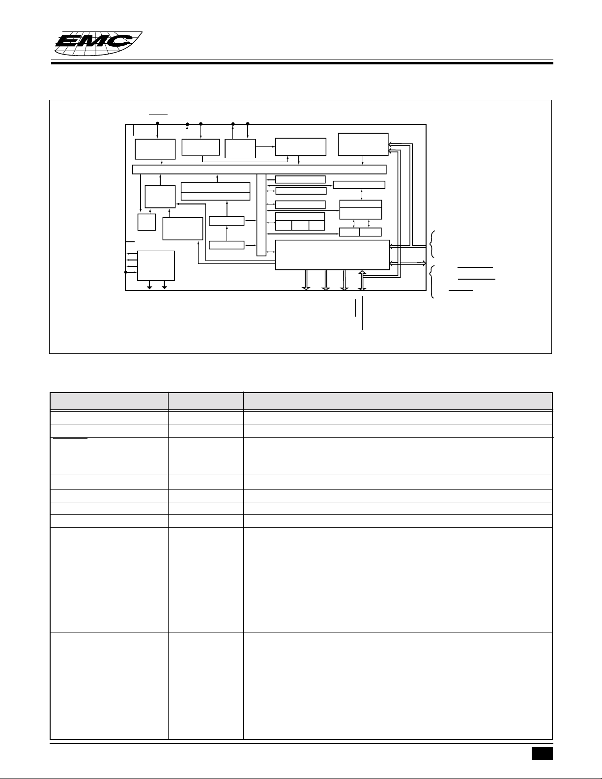
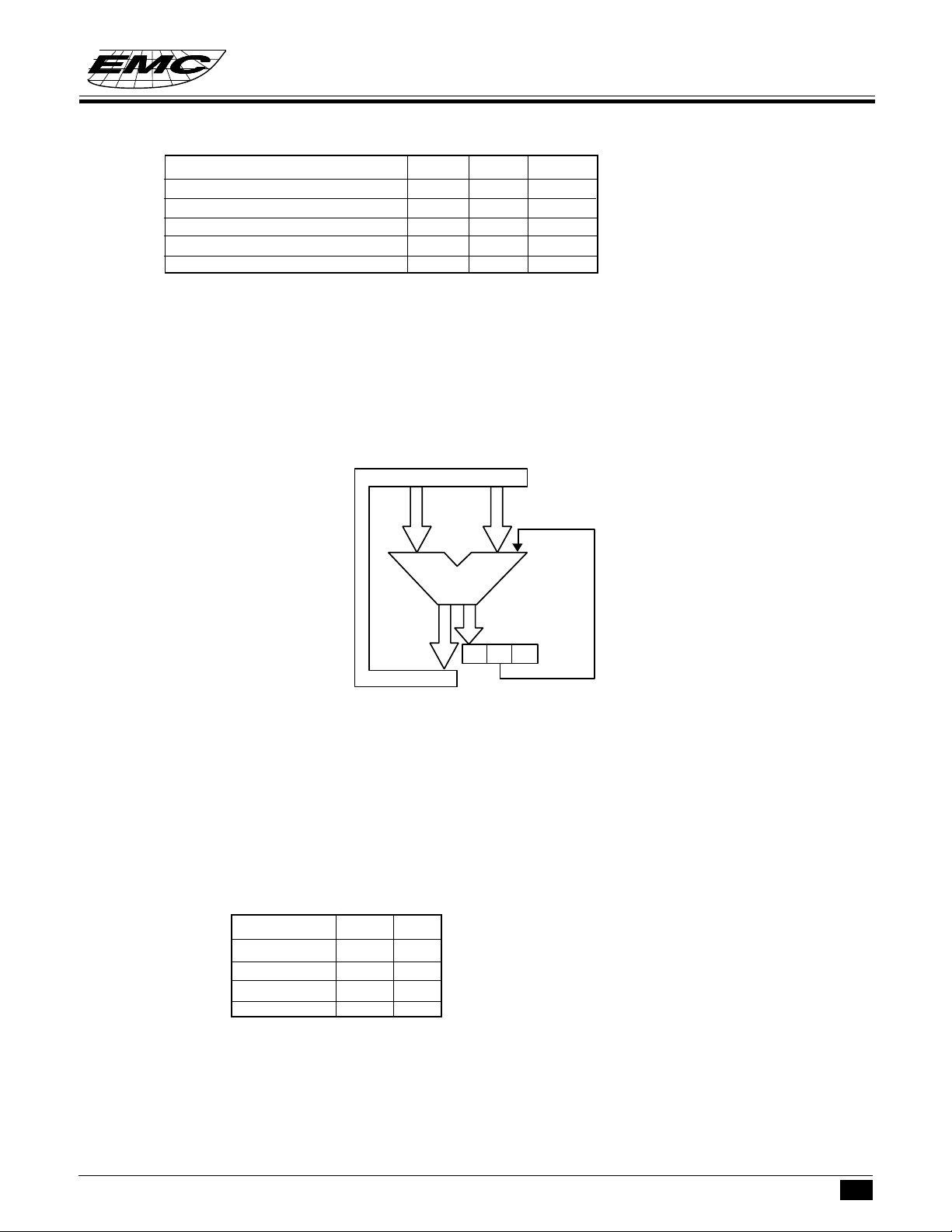
FUNCTION BLOCK DIAGRAM
EM73866
4-BIT MICRO-CONTROLLER FOR LCD PRODUCT
LXOUT
Generator
ROM
PC
LXIN
Clock
(slow)
System Control
Data Bus
Timing
Generator
Data pointer
ACC
ALU
Flag
ZCS
I/O Control
P1.0 - P1.1
Stack pointer
HR
P3.0 - P3.3
P6.0 - P6.1
Sleep Mode
Control
Stack
RAM
LR
WAKEUPA,C
P8(0,2)(INT1,0)/
P0(0..3)/WAKEUP(0..3)
P2(0..3)/WAKEUP(4..7)
P4(0..3)
P5(0..3)
/WAKEUPD
P7.0
VSS
/WAKEUP(P8..11)
/WAKEUP(P12..15)
TEST
V
RLC
Generator
(TA,TB)
XINXOUT
Clock
Instruction Decoder
Instruction Register
RESET
VDD
Reset
Control
Interrupt
Control
Time
Timer/Counter
Base
V1
V2
V3
LCD
SEG0~SEG29
COM0~COM3
PIN DESCRIPTIONS
Symbol Pin-type Function
V
DD
V
SS
RESET RESET-A System reset input signal, low active
XIN/RCOSC OSC-A/OSC-H1 Crystal/RC clock source connecting pin
XOUT OSC-A Crystal connecting pin
LXIN OSC-B/OSC-H2 Crystal/RC connecting pin for low speed clock source
LXOUT OSC-B Crystal connecting pin for low speed clock source
P0(0..3)/WAKEUP(0..3) INPUT-K 8-bit input pins with IDLE/STOP releasing function
P2(0..3)/WAKEUP(4..7) mask option : wakeup enable, negative edge release, pull-up
P1(0..1) I/O-Z 2-bit bidirection I/O pins with high current function source
Power supply (+)
Power supply (-)
mask option : none
pull-up
wakeup enable, negative edge release, none
wakeup enable, positive edge release, pull-down
wakeup enable, positive edge release, none
wakeup disable, pull-up
wakeup disable, pull-down
wakeup disable, none
mask option 1: initial low
initial high
mask option 2: low current push-pull
normal current push-pull
high current push-pull
NMOS open-drain
PMOS open-drain
* This specification are subject to be changed without notice.
12.29.1999
2
EM73866
4-BIT MICRO-CONTROLLER FOR LCD PRODUCT
PIN DESCRIPTIONS
Symbol Pin-type Function
P3(0,1)/SEG(30,31) I/O-O 2-bit bidirection I/O pins are shared with LCD segment pin
mask option : segment pin
low current push-pull
normal current push-pull
open-drain
P3(2,3), P6(0,1) I/O-N 4-bit bidirection I/O pins
mask option : low current push-pull
normal current push-pull
open-drain
P4.0/SOUND/WAKEUP8 I/O-R1 1-bit bidirection I/O with inverse sound output and IDLE/STOP
releasing function.
mask option : wakeup disable, low current push-pull
wakeup disable, normal current push-pull
wakeup disable, high current push-pull
wakeup disable, open-drain
wakeup disable, SOUND
wakup enable, low current push-pull
wakeup enable, normal current push-pull
P4.1(TRGH)/WAKEUP9 I/O-R1 1-bit bidirection I/O with HTC output and IDLE/STOP releasing
function.
mask option : wakeup disble, low current push-pull
wakeup disable, normal current push-pull
wakeup disable, high current push-pull
wakeup disable, NMOS open-drain
wakeup disable, PMOS open-drain
wakeup enable, low current push-pull
wakeup enable, normal current push-pull
P4(2,3)/WAKEUP(10,11) I/O-R1 2-bit bidirection I/O pins with IDLE/STOP releasing function
mask option : wakeup disble, low current push-pull
wakeup disable, normal current push-pull
wakeup disable, high current push-pull
wakeup disable, NMOS open-drain
wakeup disable, PMOS open-drain
wakeup enable, low current push-pull
wakeup enable, normal current push-pull
P5(0..3)/WAKEUP(12..15) I/O-S 4-bit bidirection I/O pins with IDLE/STOP releasing function
mask option : wakeup disable, low current push-pull
wakeup disable, normal current push-pull
wakeup disable, open-drain
wakeup enable, low current push-pull
wakeup enable, normal current push-pull
P7.0/TRGA/WAKEUPD I/O-S 2-bit bidirection I/O pins with timer/counterA, B external intput and
P8.1/TRGB/WAKEUPB IDLE/STOP releasing function
mask option : wakeup disable, low current push-pull
wakeup disable, normal current push-pull
wakeup disable, open-drain
wakeup enable, low current push-pull
wakeup enable, normal current push-pull
* This specification are subject to be changed without notice.
12.29.1999
3

4-BIT MICRO-CONTROLLER FOR LCD PRODUCT
PIN DESCRIPTIONS
Symbol Pin-type Function
P8.0(INT1)/WAKEUPA I/O-S 2-bit bidirection I/O pins with interrupt 0, 1 external intput and
P8.2(INT0)/WAKEUPC IDLE/STOP releasing function
mask option : wakeup disable, low current push-pull
wakeup disable, normal current push-pull
wakeup disable, open-drain
wakeup enable, low current push-pull
wakeup enable, normal current push-pull
COM(0..3) -- LCD common pins
SEG(0..29) -- LCD segment pins
V1, V2, V3, V
RLC
-- LCD bias pins
EM73866
FUNCTION DESCRIPTIONS
PROGRAM ROM ( 8K X 8 bits )
8 K x 8 bits program ROM contains user's program and some fixed data.
The basic structure of the program ROM may be categorized into 5 partitions.
1. Address 0000h: Reset start address.
2. Address 0002h - 000Ch : 6 kinds of interrupt service routine entry addresses.
3. Address 000Eh - 0086h : SCALL subroutine entry address, only available at 000Eh, 0016h, 001Eh, 0026h, 002Eh,
0036h, 003Eh, 0046h, 004Eh, 0056h, 005Eh, 0066h, 006Eh, 0076h, 007Eh, 0086h.
4. Address 0000h - 07FFh : LCALL subroutine entry address.
5. Address 0000h - 1FFFh : Except used as above function, the other region can be used as user's program and
data region.
* This specification are subject to be changed without notice.
12.29.1999
4
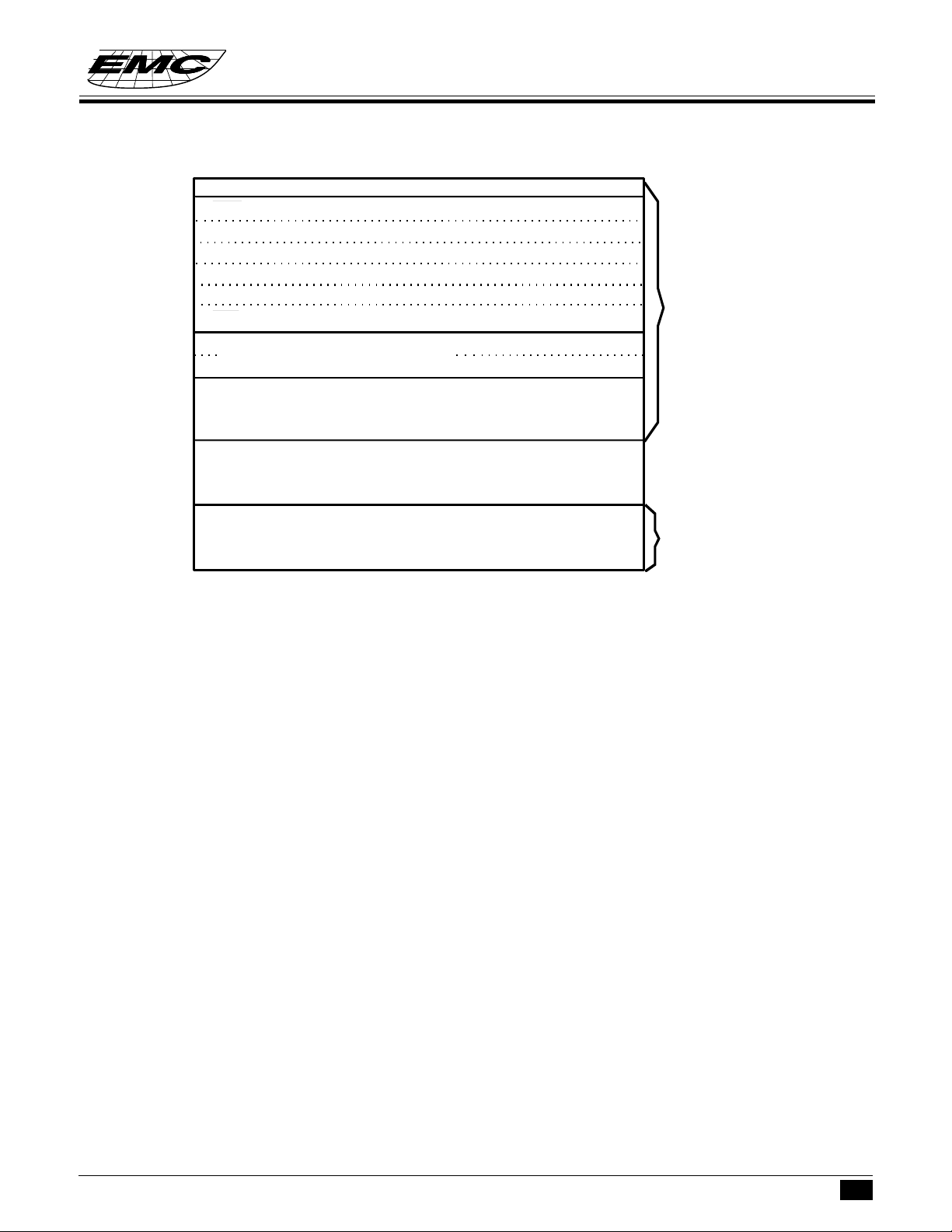
address 8192 x 8 bits
0000h
0002h
0004h
0006h
0008h
000Ah
000Ch
000Eh
0086h
07FFh
0800h
0FFFh
1000h
1FFFh
Reset start address
INT0 ; External interrupt service routine entry address
HTCI; High speed counter interrupt service routine entry address
TRGA; Timer/counterA interrupt serice routine entry address
TRGB; Timer/counterA interrupt serice routine entry address
TBI; Time base interrupt serice routine entry address
INT1; External interrupt serice routine entry address
SCALL, subroutine call entry address
.
.
.
EM73866
4-BIT MICRO-CONTROLLER FOR LCD PRODUCT
Subroutine call entry address
designated by [LCALL a]
instruction
Data table for
[LDAX],[LDAXI]
instruction
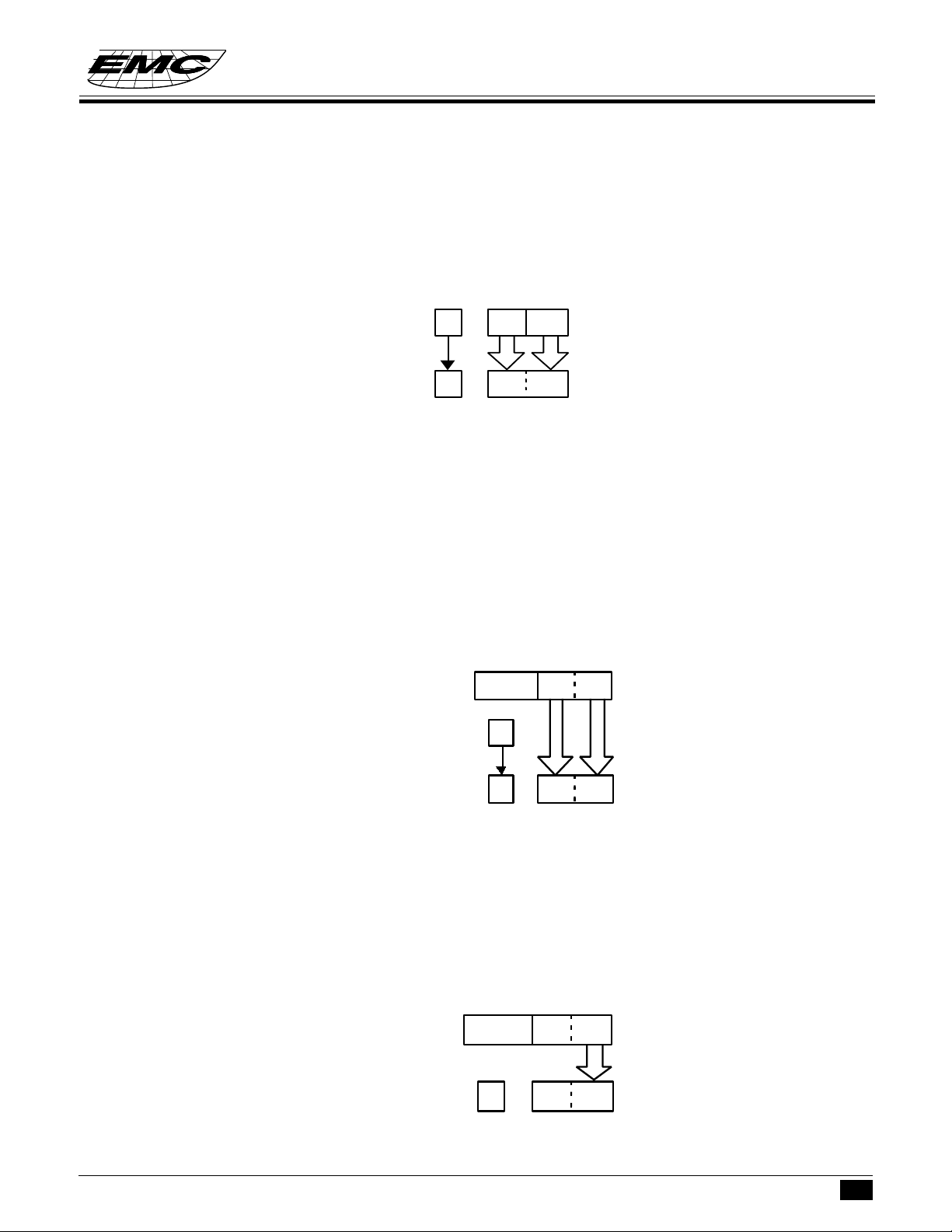
DP is a 12-bit data register that stores the program ROM address as pointer for the ROM code data.
User has to initially load ROM address into DP with instructions "STADPL", and "STADPM, STADPH",
then then to obtain the lower nibble of ROM code data by instruction "LDAX" and higher nibble by instruction
"LDAXI"
PROGRAM EXAMPLE: Read out the ROM code of address 1777h by table-look-up instruction.
LDIA #07h;
STADPL ; [DP]
STADPM ; [DP]
STADPH ; [DP]
← 07h
L
← 07h
M
← 07h, Load DP=777h
H
:
LDL #00h;
LDH #03h;
LDAX ; ACC ← 6h
STAMI ; RAM[30] ← 6h
LDAXI ; ACC ← 5h
STAM ; RAM[31] ← 5h
;
ORG 1777h
DATA 56h;
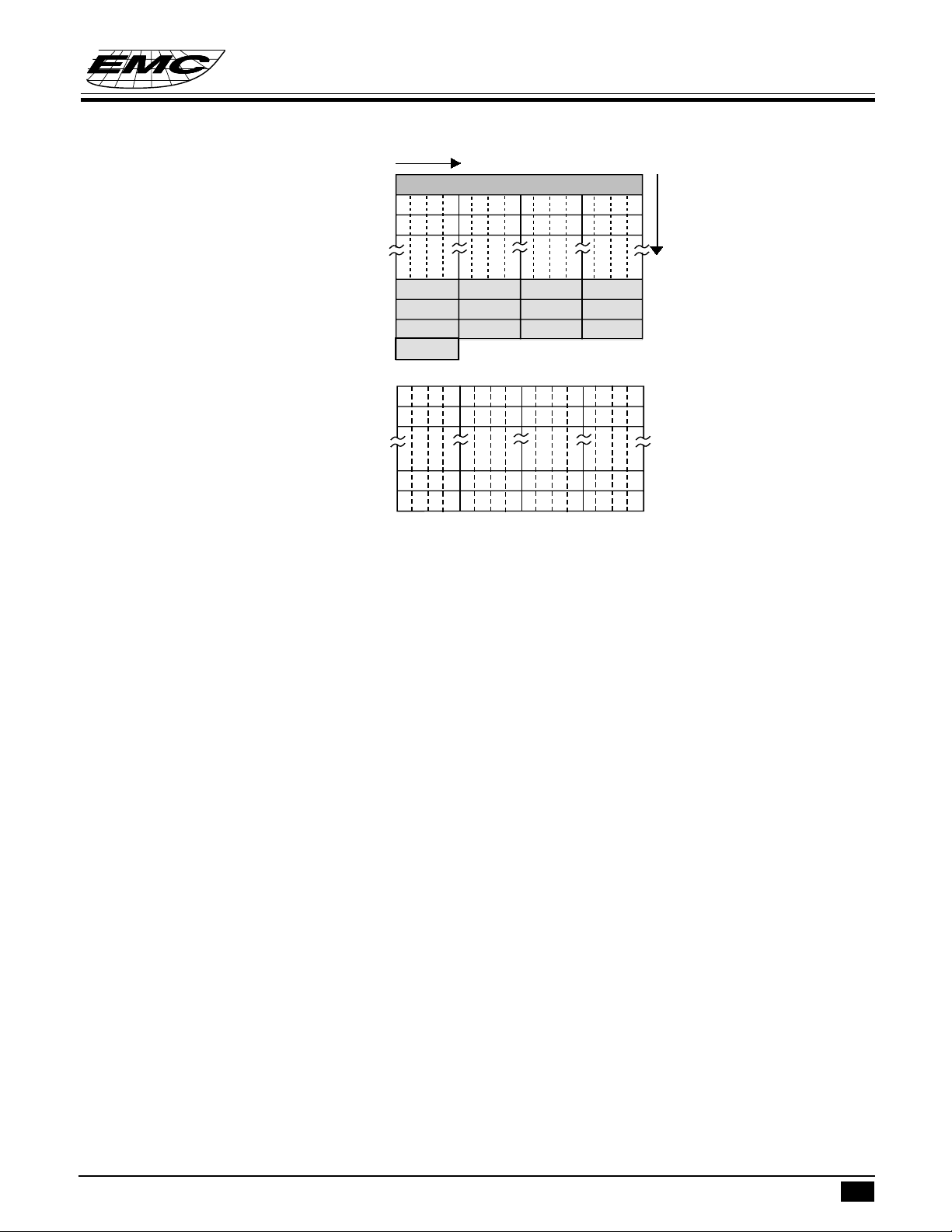
DATA RAM ( 500-nibble )
A total 500-nibble data RAM is available from address 000 to 1FFh. DATA RAM includes the zero page region,
stacks and data areas.
* This specification are subject to be changed without notice.
12.29.1999
5
EM73866
4-BIT MICRO-CONTROLLER FOR LCD PRODUCT
:
:
:
:
:
:
:
:
:
Increment
Level 0
Level 4
Level 8
Level 12
Zero-page
Level 1
Level 5
Level 9
Level 2
Level 6
Level 10
Increment
Level 3
Level 7
Level 11
Bank 0
Bank 1
Address
000h - 00Fh
010h - 01Fh
020h - 02Fh
0C0h - 0CFh
0D0h - 0DFh
0E0h - 0EFh
0F0h - 0F3h
100h - 10Fh
110h - 11Fh
1F0h - 1FFh
ZERO- PAGE:
From 000h to 00Fh is the zero-page location. It is used as the zero-page address mode pointer for the
instruction of "STD #k,y; ADD #k,y; CLR y,b; CMP k,y".
PROGRAM EXAMPLE: To write immediate data "07h" to RAM [03] and to clear bit 2 of RAM [0Eh].
STD #07h, 03h ; RAM[03] ← 07h
CLR 0Eh,2 ; RAM[0Eh]
← 0
2
STACK:
There are 13 (maximum) stack levels that user can use for subroutine (including interrupt and CALL).
User can assign any level be the starting stack by providing the level number to stack pointer (SP).
When an instruction (CALL or interrupt) is invoked, before enter the subroutine, the previous PC address
is saved into the stack until returned from those subroutines, the PC value is restored by the data saved in stack.
SPECIAL PURPOSE REGISTER:
The instruction concerning with "Timer/counter", "Data Pointer" and "Stack Pointer" at instruction table 14
be sure the RAM bank must be set in Bank0.
DATA AREA:
Except the area used by user's application, the whole RAM can be used as data area for storing and loading
general data.
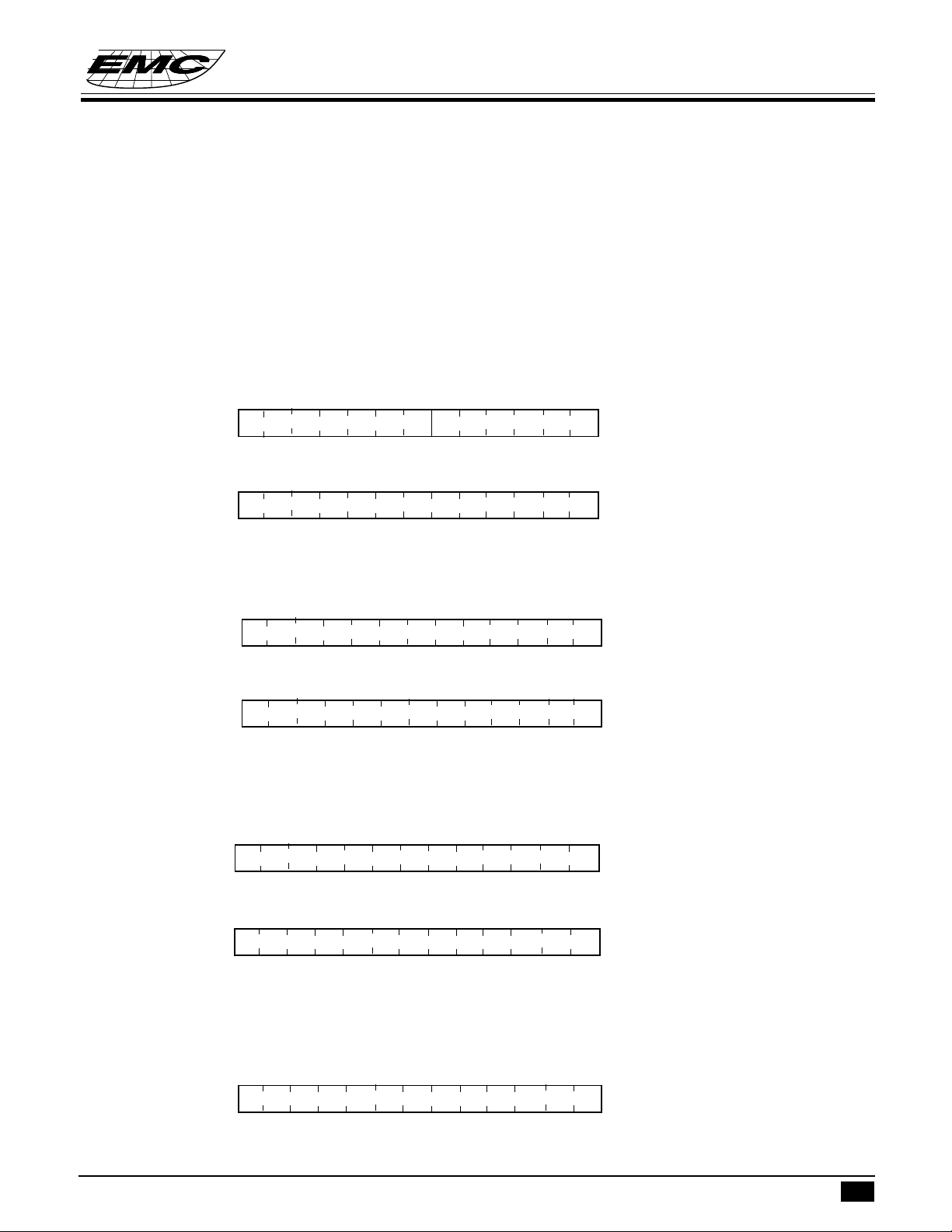
ADDRESSING MODE
The 500 nibble data memory consists of two banks (bank 0 and bank 1). There are 244x4 bits (address
000h~0F3h) in bank 0 and 256x4 bits (address 100h~1FFh) in bank 1.
* This specification are subject to be changed without notice.
12.29.1999
6
EM73866
4-BIT MICRO-CONTROLLER FOR LCD PRODUCT
The bank is selected by P9.3. When P9.3 is cleared to "0", the bank 0 is selected. When P9.3 is set to "1", the bank
1 is selected.
There are 3 addressing mode to access the data memory, namely -
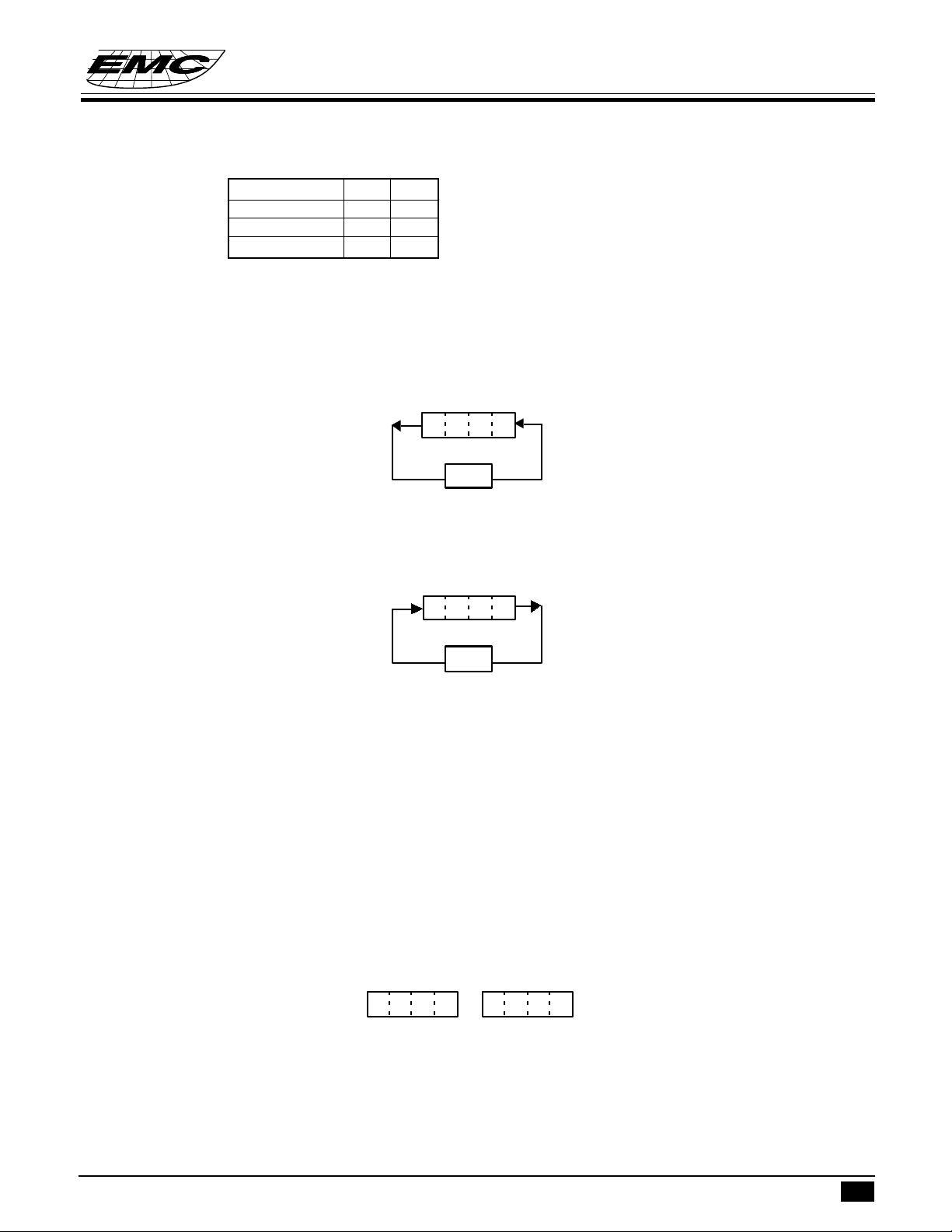
(1) Indirect addressing mode:
The address in the certain bank is specified by the HL registers.
P9.3 HR LR
RAM address
PROGRAM EXAMPLE: Load the data of RAM address "143h" to RAM address "032h".
SEP P9,3 ; P9.3← 1
LDL #3h ; LR← 3
LDH #4h ; HR← 4
LDAM ; Acc← RAM[143h]
CLP P9,3 ; P9.3← 0
LDL #2h ; LR← 2
LDH #3h ; HR← 3
STAM ; RAM[032h]← Acc
(2) Direct addressing mode:
The address in the bank is directly specified by 8 bits code of the second byte in the instruction field.
instruction field
xxxxxxxx
P9.3
RAM address
PROGRAM EXAMPLE: Load the data of RAM address "143h" to RAM address "023h".
SEP P9,3 ; P9.3← 1
LDA 43 h ; Acc← RAM[143h]
CLP P9,3 ; P9.3← 0
STA 23h ; RAM[023h]← Acc
(3) Zero-page addressing mode:
The address is the lower 4 bits code of the second byte in the instruction field.This kind of instructions are
only available for the zero page. Area in bank0, even the P9.3 is set.
xxxxxxxx
instruction field
yyyy
RAM address
0
PROGRAM EXAMPLE: Write immediate "0Fh" to RAM address "005h".
STD #0Fh, 05h ; RAM[05h]← 0Fh
* This specification are subject to be changed without notice.
0000
yyyy
12.29.1999
7
EM73866
4-BIT MICRO-CONTROLLER FOR LCD PRODUCT
PROGRAM COUNTER (8K ROM)
Program counter ( PC ) is composed by a 13-bit counter, which indicates the next executed address for the
instruction of program ROM instruction.
For BRANCH and CALL instructions, PC is changed by instruction indicated. PC can only indicate the address
from 0000h-1FFFh.
(1) Branch instruction:
SBR a
Object code: 00aa aaaa
Condition: SF=1; PC ← PC
PC Hold original PC value+1 aaaaaa
SF=0; PC← PC +1( branch condition not satisified)
PC Original PC value + 1
( branch condition satisified )
12-6.a
LBR a
Object code: 1100 aaaa aaaa aaaa
Condition: SF=1; PC ← PC
Hold
PC
a a a a a a aaaaaa
+2
( branch condition satisified )
12.a
SF=0; PC← PC +2( branch condition not satisified)
PC Original PC value + 2
SLBR a
Object code: 0101 0101 1100 aaaa aaaa aaaa (a:1000h~1FFFh)
0101 0111 1100 aaaa aaaa aaaa (a:0000h~0FFFh)
Condition: SF=1; PC ← a ( branch condition satisified )
PCaaaaaaaaaaaa a
SF=0 ; PC ← PC + 3 ( branch condition not satisified )
PC Original PC value + 3
(2) Subrountine instruction:
SCALL a
Object code: 1110 nnnn
Condition : PC ← a ; a=8n+6 ; n=1..Fh ; a=86h, n=0
PC00000aaaaa aaa
* This specification are subject to be changed without notice.
12.29.1999
8
4-BIT MICRO-CONTROLLER FOR LCD PRODUCT
LCALL a
Object code: 0100 0aaa aaaa aaaa
Condition: PC ← a
PC00aaaaaaaaaa a
RET
Object code: 0100 1111
Condition: PC ← STACK[SP]; SP + 1
PC The return address stored in stack
RT I
Object code: 0100 1101
Condition : FLAG. PC ← STACK[SP]; EI ← 1; SP + 1
PC The return address stored in stack
EM73866
(3) Interrupt acceptance operation:
When an interrupt is accepted, the original PC is pushed into stack and interrupt vector will be loaded into
PC,The interrupt vectors are as following:
INT0 (External interrupt from P8.2)
PC0000000000010
TRGH (High speed counter interrupt)
PC0000000000100
TRGA (Timer A overflow interrupt)
PC0000000000110
TRGB (Time B overflow interrupt)
PC0000000001000
TBI (Time base interrupt)
PC0000000001010
INT1 (External interrupt from P8.0)
PC0000000001100
(4) Reset operation:
PC000000000000 0
* This specification are subject to be changed without notice.
12.29.1999
9
EM73866
4-BIT MICRO-CONTROLLER FOR LCD PRODUCT
(5) Other operations:
For 1-byte instruction execution: PC + 1
For 2-byte instruction execution: PC + 2
For 3-byte instruction execution: PC + 3
ACCUMULATOR
Accumulator is a 4-bit data register for temporary data. For the arithematic, logic and comparative opertion
.., ACC plays a role which holds the source data and result.
FLAGS
There are 3 kinds of flag, CF ( Carry flag ), ZF ( Zero flag ), SF ( Status flag ), these 3 1-bit flags are affected
by the arithematic, logic and comparative .... operation.
All flags will be put into stack when an interrupt subrountine is served, and the flags will be restored after
RTI instruction executed.
(1) Carry Flag ( CF )
The carry flag is affected by following operation :
a. Addition : CF as a carry out indicator, when the addition operation has a carry-out, CF will be "1", in
another word, if the operation has no carry-out, CF will be "0".
b. Subtraction : CF as a borrow-in indicator, when the subtraction operation must has a borrow-in, the CF
will be "0", in another word, if no borrow-in, CF will be "1".
c. Comparision : CF is as a borrow-in indicator for Comparision operation as the same as subtraction
operation.
d. Rotation : CF shifts into the empty bit of accumulator for the rotation and holds the shift out data after
rotation.
e. CF test instruction : For TFCFC instruction, the content of CF sends into SF then clear itself "0".
For TTSFC instruction, the content of CF sends into SF then set itself "1".
(2) Zero Flag ( ZF )
ZF is affected by the result of ALU, if the ALU operation generate a "0" result, the ZF will be "1", otherwise,
the ZF will be "0".
(3) Status Flag ( SF )
The SF is affected by instruction operation and system status.
a. SF is initiated to "1" for reset condition.
b. Branch instruction is decided by SF, when SF=1, branch condition will be satisified, otherwise, branch
condition will not be satisified by SF = 0.
PROGRAM EXAMPLE:
Check following arithematic operation for CF, ZF, SF
* This specification are subject to be changed without notice.
12.29.1999
10
EM73866
4-BIT MICRO-CONTROLLER FOR LCD PRODUCT
CF ZF SF
LDIA #00h; - 1 1
LDIA #03h; - 0 1
ADDA #05h; - 0 1
ADDA #0Dh; - 0 0
ADDA #0Eh; - 0 0
ALU
The arithematic operation of 4-bit data is performed in ALU unit. There are 2 flags can be affected by the
result of ALU operation, ZF and SF. The operation of ALU can be affected by CF only.
ALU STRUCTURE
ALU supported user arithematic operation function, including : addition, subtraction and rotaion.
DATA BUS
ALU
ZF CF SF
ALU FUNCTION
(1) Addition:
For instruction ADDAM, ADCAM, ADDM #k, ADD #k,y .... ALU supports additional function.
The additional operation can affect CF and ZF. For additional operation, if the result is "0", ZF will be
"1", otherwise, not equal "0", ZF will be "0". When the addition operation has a carry-out, CF will be "1",
otherwise, CF will be "0".
EXAMPLE:
Operation Carry Zero
3+4=7 0 0
7+F=6 1 0
0+0=0 0 1
8+8=0 1 1
(2) Subtraction:
For instruction SUBM #k, SUBA #k, SBCAM, DECM... ALU supports user subtraction function. The
subtraction operation can affect CF and ZF, For subtraction operation, if the result is negative, CF will
be "0", it means a borrow out, otherwise, if the result is positive, CF will be "1". For ZF, if the result
of subtraction operation is "0", the ZF will be "1", otherwise, ZF will be "1".
* This specification are subject to be changed without notice.
12.29.1999
11
EM73866
4-BIT MICRO-CONTROLLER FOR LCD PRODUCT
EXAMPLE:
Operation Carry Zero
8-4=4 1 0
7-F= -8(1000) 0 0
9-9=0 1 1
(3) Rotation:
There are two kinds of rotation operation, one is rotation left, the other is rotation right.
RLCA instruction rotates Acc value to left, shift the CF value into the LSB bit of Acc and the shift out data
will be hold in CF.
MSB LSB
ACC
CF
RRCA instruction operation rotates Acc value to right, shift the CF value into the MSB bit of Acc and the
shift out data will be hold in CF.
MSB LSB
ACC
CF
PROGRAM EXAMPLE: To rotate Acc right and shift a "1" into the MSB bit of Acc.
TTCFS; CF ← 1
RRCA; rotate Acc right and shift CF=1 into MSB.
HL REGISTER
HL register are two 4-bit registers, they are used as a pair of pointer for the address of RAM memory and also
2 independent temporary 4-bit data registers. For some instruction, L register can be a pointer to indicate the
pin number (Port4).
HL REGISTER STRUCTURE
3 2 1 0
3 2 1 0
H REGISTER
* This specification are subject to be changed without notice.
L REGISTER
12.29.1999
12
 Loading...