ELAN EM19110M Datasheet

10-BIT 5 MSPS A/D CONVERTER
10-BIT 5 MSPS A/D CONVERTER
GENERAL DESCRIPTION
EM19110 is a 10-bit, 5 MHZ CMOS A/D converter for high speed and high resolution use. The 2-step parallel
structures accompanying with an average technique that external generated reference voltage, the users can tune
transfer curve to meet their application.
FEATURES
• 5 MSPS maximum conversion speed
• High resolution up to 10 bit
• Built-in sampling and hold circuit
• Internal self-bias reference voltage
• 115 mW low power dissipation at 5MSPS
• +5V single power supply
• Available in 24 pin SOP
• Series
EM19110M for 300 mil SOP
EM19110
EM19110
APPLICATION
Precision scanner, digital cellular phone and a wide range of fields where high speed and high resolution A/D
conversion is required in the digital communication.
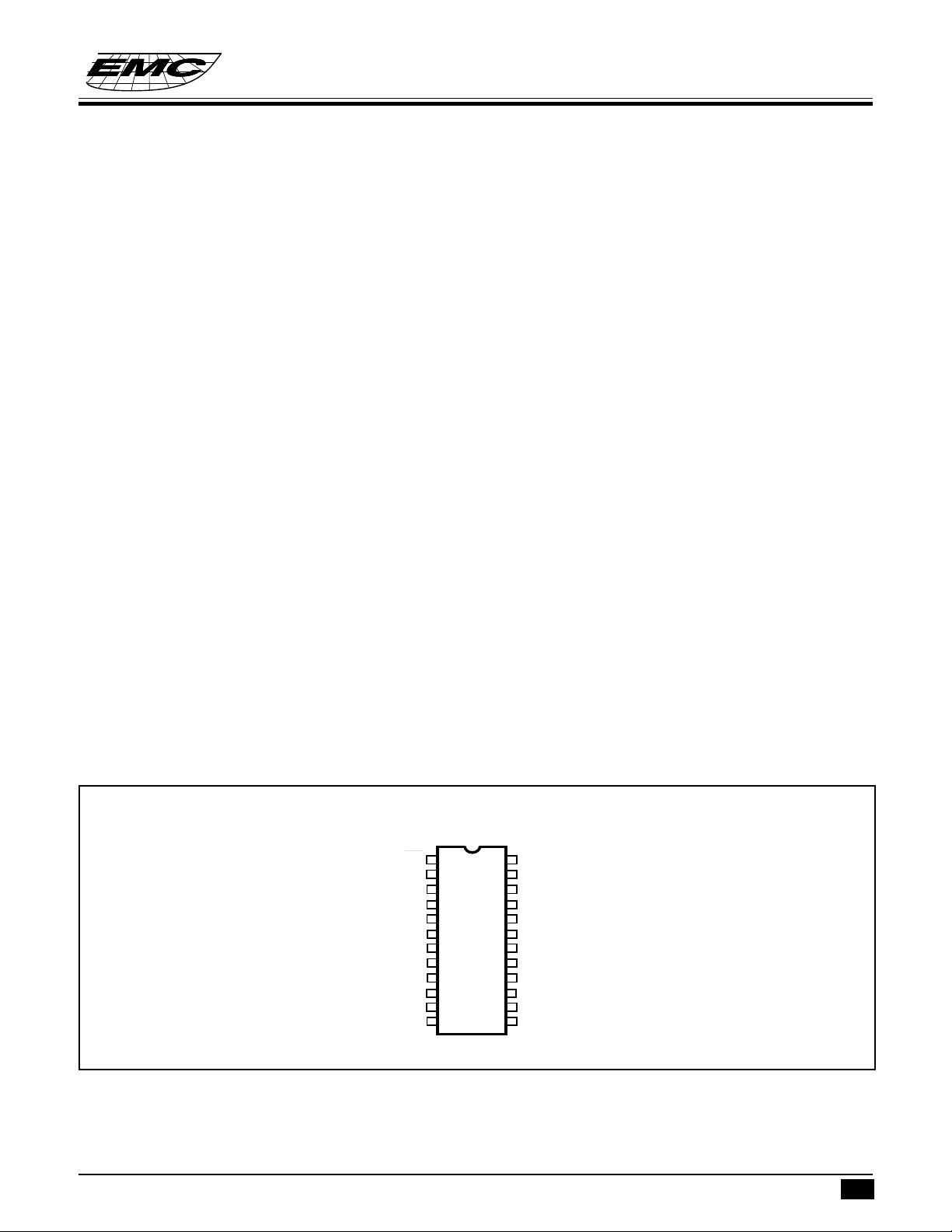
PIN ASSIGNMENT
EM19110
OE
D0(LSB)
D1
D2
D3
D4
D5
D6
D7
D8
D9(MSB)
CLK
1
2
3
4
5
6
7
8
9
10
11
12
DVSS
24
VRB
23
VRBS
22
AR1
21
AVSS
20
VIN
19
AVDD
18
VR2
17
VR3
16
VRT
15
VRTS
14
DVDD
13
* This specification are subject to be changed without notice.
5.26.1997
1

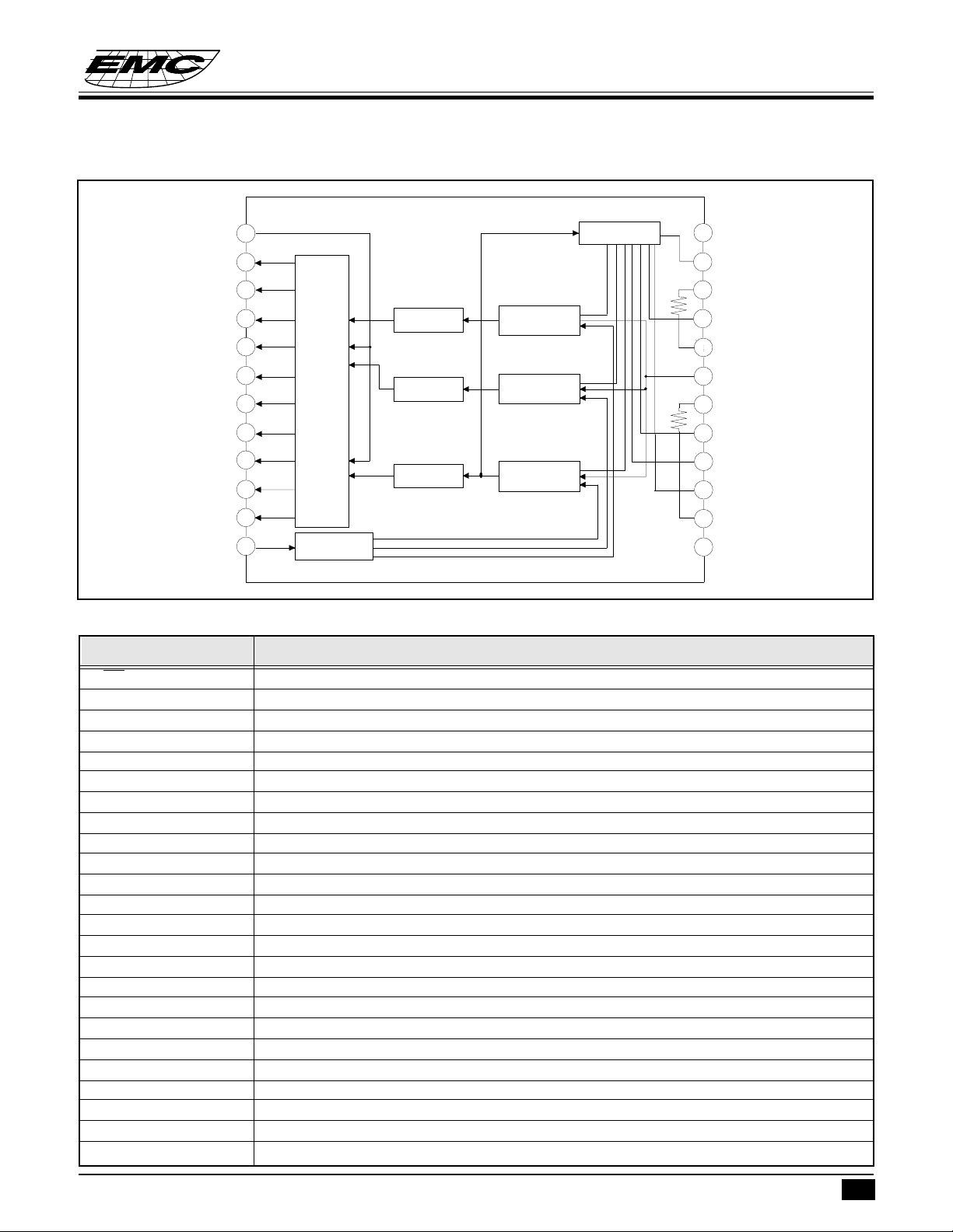
FUNCTIONAL BLOCK DIAGRAM
EM19110
10-BIT 5 MSPS A/D CONVERTER
1
/OE
D0
2
D1
3
D2
4
D3
5
D4
6
D5
7
D6
8
D7
9
D8
10
D9
11
12
CLK DVDD
Error
correction
and
data
latches
Clock center
Fine encoder
Fine encoder
Coarse encoder
Fine
Comparators with
S/ H (6bit)
Fine
Comparators with
S/ H (6bit)
Coarse
Comparators with
S/ H (4bit)
PIN DESCRIPTIONS
Symbol Function
OE Output enable
D0 Data output bit 0 (LSB)
D1 Data output bit 1
D2 Data output bit 2
D3 Data output bit 3
D4 Data output bit 4
D5 Data output bit 5
D6 Data output bit 6
D7 Data output bit 7
D8 Data output bit 8
D9 Data output bit 9 (MSB)
CLK Clock input
DVDD Digital power supply
VRTS Top internal reference voltage
VRT Top reference voltaget
VR3 Tap-3 reference voltage
VR2 Tap-2 reference voltage
AVDD Analog power supply
VIN Analog input voltage
AVSS Analog ground
VR-1 Tap-1 reference voltage
VRBS Bottom internal reference voltage
VRB Bottom reference voltage
DVSS Digital ground
Ladder resistors
DVSS
24
VRB
23
VRBS
22
21
VR1
20
AVSS
VIN
19
AVDD
18
17
VR2
VR3
16
VRT
15
14
VRTS
13
* This specification are subject to be changed without notice.
5.26.1997
2
 Loading...