ELAN EM19101S, EM19101M Datasheet

8-BIT 5 MSPS A/D CONVERTER (CMOS)
8-BIT 5 MSPS A/D CONVERTER (CMOS)
GENERAL DESCRIPTION
EM19101 is a 8-bit CMOS A/D converter for scanner use. The adoption of a 2-step parallel system achieves low
consumption at a maximum conversion speed of 7 MSPS.
FEATURES
• 7MSPS maximum conversion speed
• Build-in sampling and hold circuit
• Internal self-bias reference voltage
• 45 mW very low power dissipation at 5MSPS
• +5V single power supply
• Available in 24 pin SOP
• Series
EM19101M for 300 mil SOP
EM19101S for 209 mil SOP
EM19101
EM19101
APPLICATION
Scanner and a wide range of fields where high speed A/D conversion is required in the digital communication.
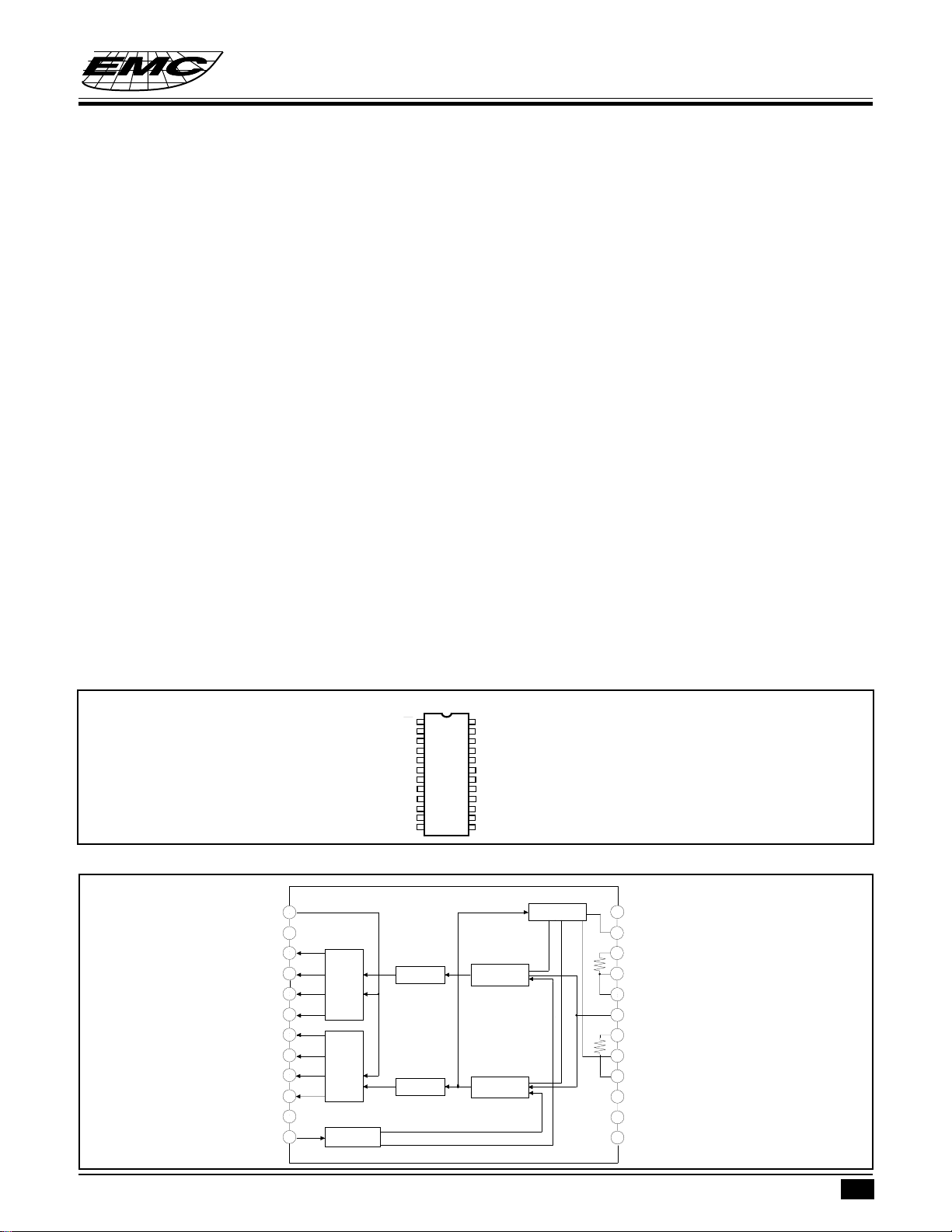
PIN ASSIGNMENT
EM19101
DVSS
DVDD
CLK
OE
1
2
D0
3
D1
4
D2
5
D3
6
D4
7
D5
8
D6
9
D7
10
11
12
DVSS
24
VRB
23
VRBS
22
AVSS
21
AVSS
20
VIN
19
AVDD
18
VRT
17
VRTS
16
AVDD
15
AVDD
14
DVDD
13
FUNCTIONAL BLOCK DIAGRAM
DVSS
1
/OE
DVSS
2
D0
3
D1
4
Lower data
D2
5
D3
6
D4
7
D5
8
D6
9
D7
10
DVDD
11
12
CLK DVDD
latches
Upper data
latches
Clock generator
Lower encoder
(4bit)
Upper encoder
(4bit)
Comparators with
S/ H (4bit)
Comparators with
S/ H (4bit)
Reference voltage
Lower
Upper
24
VRB
23
VRBS
22
21
AVSS
20
AVSS
VIN
19
AVDD
18
17
VRT
VRTS
16
AVDD
15
14
AVDD
13
* This specification are subject to be changed without notice.
4.23.1997
1

PIN DESCRIPTIONS
N-3
N-2
N
N+1
N+2
N+3
N+4
N-1
N N+1
N+2
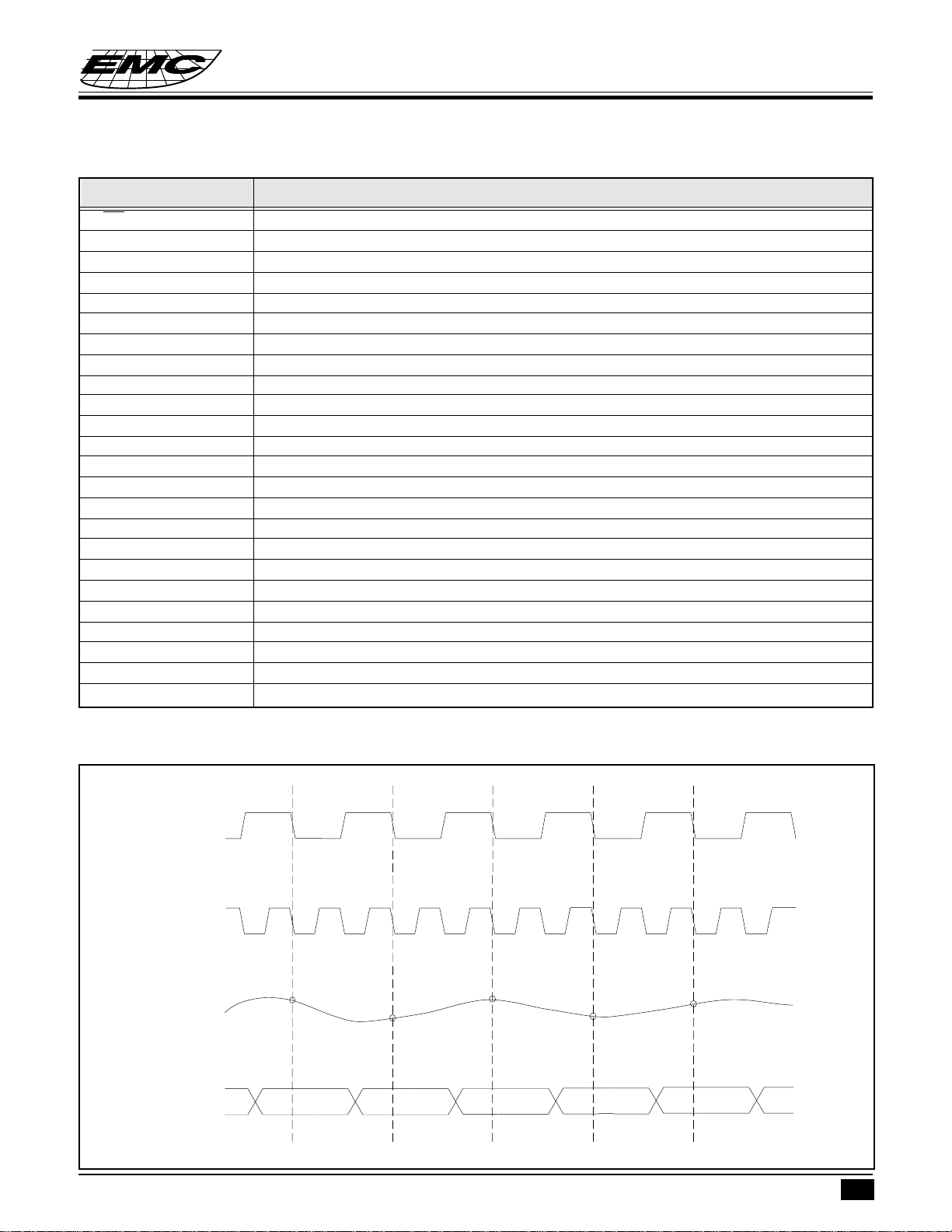
Clock
Analog input
Data output
External
Clock
Transf er
Symbol Function
OE Output enable
DVSS Digital ground
D0 Data output bit 0 (LSB)
D1 Data output bit 1
D2 Data output bit 2
D3 Data output bit 3
D4 Data output bit 4
D5 Data output bit 5
D6 Data output bit 6
D7 Data output bit 7 (MSB)
DVDD Digital power supply
CLK Clock input
DVDD Digital power supply
AVDD Analog power supply
AVDD Analog power supply
VRTS Top internal reference voltage
VRT Top reference voltaget
AVDD Analog power supply
VIN Analog input voltage
AVSS Analog ground
AVSS Analog ground
VRBS Bottom internal reference voltage
VRB Bottom reference voltage
DVSS Digital ground
EM19101
8-BIT 5 MSPS A/D CONVERTER (CMOS)
TIMING DIAGRAM
* This specification are subject to be changed without notice.
4.23.1997
2
 Loading...