

RBV1000 - RBV1010
FEATURES :
* High current capability
* High surge current capability
* High reliability
* Low forward voltage drop
* High case dielectric strength of 2000 V
* Ideal for printed circuit board
* Very good heat dissipation
MECHANICAL DATA :
* Case : Reliable low cost construction
utilizing molded plastic technique
* Epoxy : UL94V-O rate flame retardant
* Terminals : Plated lead solderable per
MIL-STD-202, Method 208 guaranteed
* Polarity : Polarity symbols marked on case
* Mounting position : Any
* Weight : 7.7 grams
MAXIMUM RATINGS AND ELECTRICAL CHARACTERISTICS
Rating at 25
C ambient temperature unless otherwise specified.
For capacitive load, derate current by 20%.
I2t
A2S
Notes :
1. Thermal Resistance from junction to case with units mounted on a 3.2" x 3.2" x 0.12" (8.2cm.x 8.2cm.x 0.3cm.) Al.-Finned Plate.
UPDATE : NOVEMBER 1,1998
~
~
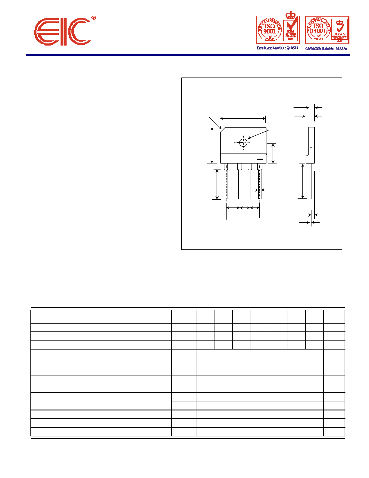
30 ± 0.3
+
PRV : 50 - 1000 Volts
Io : 10 Amperes
* Low reverse current
SILICON BRIDGE RECTIFIERS
RBV25
3.9 ± 0.2
C3
20 ± 0.3
4.9 ± 0.2
∅
3.2 ± 0.1
11 ± 0.2
DC
0.3
±
13.5
1.0 ± 0.1
±
7.5
0.2
±
7.5
0.2
2.0 ± 0.2
0.7 ± 0.1
10
±
0.2
17.5 ± 0.5
Dimensions in millimeters
°
Single phase, half wave, 60 Hz, resistive or inductive load.
RATING
SYMBOL
RBV
1000
Maximum Recurrent Peak Reverse Voltage VRRM 50 100 200 400 600 800 1000 Volts
Maximum RMS Voltage VRMS 35 70 140 280 420 560 700 Volts
Maximum DC Blocking Voltage VDC 50 100 200 400 600 800 1000 Volts
Maximum Average Forward Current Tc = 55°C I
F(AV) 10
Peak Forward Surge Current Single half sine wave
Superimposed on rated load (JEDEC Method) IFSM 300 Amps.
Current Squared Time at t < 8.3 ms.
Maximum Forward Voltage per Diode at IF = 5.0 Amps. V
Maximum DC Reverse Current Ta = 25 °C I
at Rated DC Blocking Voltage Ta = 100 °C I
Typical Thermal Resistance (Note 1)
F 1.0
R 10 µ
R(H)
RθJC
Operating Junction Temperature Range TJ - 40 to + 150
Storage Temperature Range T
STG - 40 to + 150 °
RBV
1001
RBV
1002
RBV
1004
160
200
2.5
RBV
1006
RBV
1008
RBV
1010
UNIT
Amps.
Volts
A
µ
A
°
C/W
°
C
C
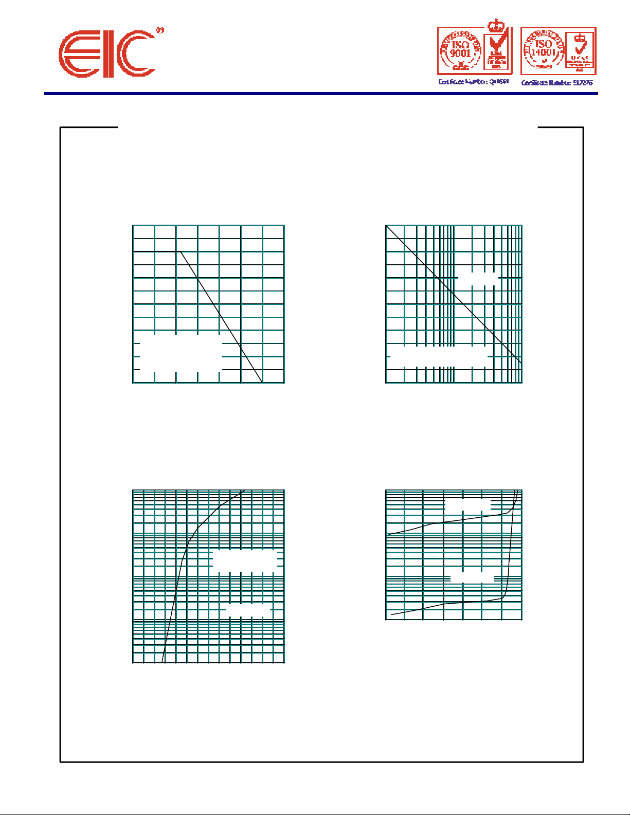
RATING AND CHARACTERISTIC CURVES ( RBV1000 - RBV1010 )
864
2
10
1.0
200
0
0
50
10
0.01
0.1
TJ = 25 °C
10
HEAT-SINK MOUNTING, Tc
FIG.1 - DERATING CURVE FOR OUTPUT FIG.2 - MAXIMUM NON-REPETITIVE PEAK
RECTIFIED CURRENT FORWARD SURGE CURRENT
12
AMPERES
300
250
TJ = 50 °C
150
AMPERES
100
3.2" x 3.2" x 0.12" THK.
(8.2cm x 8.2cm x 0.3cm)
Al.-FINNED PLATE
PEAK FORWARD SURGE CURRENT,
8.3 ms SINGLE HALF SINE WAVE
JEDEC METHOD
AVERAGE FORWARD OUTPUT CURRENT
0 25 50 75 100 125 150 175
CASE TEMPERATURE, ( °C)
2
NUMBER OF CYCLES AT 60Hz
10 20 601
4 6 40 100
FIG.3 - TYPICAL FORWARD CHARACTERISTICS FIG.4 - TYPICAL REVERSE CHARACTERISTICS
PER DIODE PER DIODE
100
TJ = 100 °C
Pulse Width = 300 µs
1 % Duty Cycle
1.0
MICROAMPERES
REVERSE CURRENT,
TJ = 25 °C
0.1
FORWARD CURRENT, AMPERES
40 60 120
20
PERCENT OF RATED REVERSE
80
100 1400
VOLTAGE, (%)
0.01
0.4
0.8 1.0 1.6
0.6
1.2 1.4
1.8
FORWARD VOLTAGE, VOLTS
 Loading...