

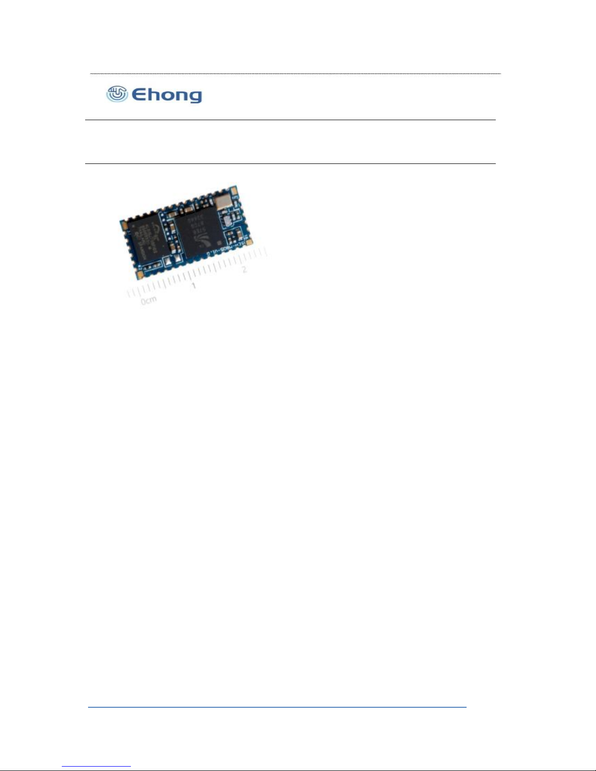
Ehong EH-MB05 User Manual
EH
-
MB05
Bluetooth® technology
audio
module
FCCID:2ACCRMB05
• Bluetooth radio
-
-
-
-
-
Fully embedded Bluetooth® v
3.0 +EDR
Class2 module
128-bit encryption security
Range up to 15m
Multipoint capability(7 transmit data devices
connected at the same time)
• Support profiles
-
-
-
SPP (Master and slave)
iAP (ipod accessory protocol)
HFP ,A2DP,AVRCP,HID(Salve)
EH-MB05
• User interface
-
Send AT command over UART
- Firmware upgrade over USB
-
With SPP service active: 560kbps tr
ansmission
speed (UART)
-
PCM interface (I2S,SPDIF)
- I2C interface(Master )
•
Audio codec
-
-
-
16bit internal stereo codec :95dB SNR for DAC
64MIPS Kalimba DSP coprocessor
Support Apt-X ,AAC, Apt-XLL,SBC codec
•
General I/O
-
-
11 general purpose I/Os
2 analogue I/O
•
FCC and Bluetooth® qualified
•
Single voltage supply: 3.3V typical
•
Small form factor: 23.24 x 11.93 x 2.2mm
•
Operating temperature range: -40 °C to 85 °C
• The operation distance >20cm
Version 2.0
July 21 2014
Shanghai Ehong Technologies Inc

Bluetooth Audio Module
1. Contents
1.
2.
3.
4.
Description
.............................................................................................................................
................................... 4
Application................................................................................................................................................................. 4
EH-MB05 Product numbering ............................................................................................................................. 4
Electrical Characteristic ........................................................................................................................................ 5
4.1. Recommend operation conditions
.............................
.................................................................................... 5
Absolute Maximum Rating
.............................................................................................................................. 5
Power consumptions ........................................................................................................................................ 6
Input/output Terminal Characteristics ........................................................................................................... 6
4.2.
4.3.
4.4.
4.4.1.
4.4.2.
4.4.3.
4.4.4.
Digital Terminals
.............................................................................................................................
........... 6
USB .............................................................................................................................................................. 7
Internal CODEC Analogue to Digital Converter ................................................................................. 7
Internal CODEC Digital to Analogue Converter ................................................................................. 8
5.
6.
Pinout and Terminal Description
..........................................................................
.............................................. 9
5.1. Pin assignment
.............................................................................................................................
..................... 9
Physical Interfaces
...................
.............................................................................................................................
11
6.1. Power Supply
.............................................................................................................
...................................... 11
Reset .................................................................................................................................................................. 12
PIO ...................................................................................................................................................................... 12
AIO
...................................................................................................................................................................... 12
UART.................................................................................................................................................................. 13
I2C Master ........................................................................................................................................................ 13
6.2.
6.3.
6.4.
6.5.
6.6.
6.6.1.
Apple iOS CP reference design
...............................................................
............................................ 14
6.7. Digital Audio Interfaces
.............................................................................................................................
..... 15
6.7.1
6.7.2
PCM
............................
.............................................................................................................................
.. 16
Digital Audio Interface (I S) .................................................................................................................. 16
2
6.7.3
IEC 60958 Interface (SPDIF)
............................................................................................................... 19
6.8 Microphone input
.............................................................
................................................................................ 20
Analog Output stage
....................................................................................................................................... 21
USB .................................................................................................................................................................... 21
6.9 6.10 7.
8.
EH-MB05 Reference Design
.........................................................
...................................................................... 23
Mechanical and PCB Footprint Characteristics.......................................................................................... 24
Shanghai Ehong Technologies Inc

Bluetooth Audio Module
RF Layout Guidelines .......................................................................................................................................... 24
9. 9.1 Feed Line and Antenna
.............................................................................................................................
..... 25
Matching network in free space ................................................................................................................... 26
9.2 10.
11.
Reflow Profile
.............................................................................................................................
........................
27
Contact Information ......................................................................................................................................... 28
2. Table of Tables
T
ABLE
1: R
ECOMMENDED OPERATING CONDITIONS
..............................
................................................................. 5
TABLE 2: ABSOLUTE MAXIMUM RATING RECOMMENDED OPERATING CONDITIONS ................................................ 5
TABLE 3: POWER CONSUMPTIONS .......................................................................................................................... 6
TABLE 4: DIGITAL TERMINAL .................................................................................................................................. 7
TABLE 5: USB TERMINAL ....................................................................................................................................... 7
TABLE 6: ANALOGUE TO DIGITAL CONVERTER ....................................................................................................... 8
TABLE 7: DIGITAL TO ANALOGUE CONVERTER ....................................................................................................... 8
T
ABLE
8:PIN T
ERMINAL DESCRIPTION
......................................
......................................................................... 11
T
ABLE
9: P
IN STATUS ON RESET
.......................................................................................................................... 12
TABLE 10: POSSIBLE UART SETTINGS ................................................................................................................ 13
TABLE 11:ALTERNATIVE FUNCTIONS OF THE DIGITAL AUDIO BUS INTERFACE ON THE PCM INTERFACE .............. 16
TABLE 12 : DIGITAL AUDIO INTERFACE SLAVE TIMING .......................................................................................... 17
TABLE 13 : DIGITAL AUDIO INTERFACE MASTER TIMING ....................................................................................... 18
TABLE 14: USB INTERFACE COMPONENT VALUES ............................................................................................... 22
3. Table of Figures
F
IGURE
1
:
P
I N OUT OF
EH-
MB05................................................................
......................................................... 9
FIGURE 2: P OW ER SUPPLY PCB DESIGN .......................................................................................................... 11
F
IGURE
3
:
C
O NNECTION TO HOST DEVICE
................
........................................................................................ 13
FIGURE 4 : EXAMPLE EEPROM CONNECTION WITH I2C INTERFACE .................................................................... 14
FIGURE 5 : APPLE CO-PROCESSOR 2.0C ............................................................................................................. 14
FIGURE 6 : APPLE CO-PROCESSOR 2.0B ............................................................................................................. 15
FIGURE 7 : AUDIO INTERFACE .............................................................................................................................. 15
FIGURE 8 : DIGITAL AUDIO INTERFACE MODES ..................................................................................................... 17
FIGURE 9 : DIGITAL AUDIO INTERFACE SLAVE TIMING .......................................................................................... 18
FIGURE 10 : DIGITAL AUDIO INTERFACE MASTER TIMING ..................................................................................... 18
FIGURE 11: EXAMPLE CIRCUIT FOR SPDIF INTERFACE (CO-AXIAL ) ..................................................................... 19
FIGURE 12: EXAMPLE CIRCUIT FOR SPDIF INTERFACE (OPTICAL) ....................................................................... 20
FIGURE 13: MICROPHONE BIASING (SINGLE CHANNEL SHOW N) ........................................................................... 20
FIGURE 14: SPEAKER OUTPUT ............................................................................................................................. 21
FIGURE 15: USB CONNECTIONS .......................................................................................................................... 22
FIGURE 16: REFERENCE DESIGN ......................................................................................................................... 23
FIGURE 17: RECOMMENDED PCB MOUNTING PATTERN (UNIT: MM, DEVIATION:0.02MM)TOP VIEW ................... 24
FIGURE 18: CLEARANCE AREA OF ANTENNA ......................................................................................................... 25
FIGURE 19: ANTENNA REFERENCE DESIGN .......................................................................................................... 26
FIGURE 20: PI MATCH NETWORK EXAMPLE ........................................................................................................... 26
FIGURE 21: RECOMMENDED REFLOW PROFILE ................................................................................................... 27
Shanghai Ehong Technologies Inc

Bluetooth Audio Module
1. Description
The EH-MB05 is an easy to use Bluetooth module, compliant with Bluetooth v3.0+EDR. The
module provides complete RF platform in a small form factor.
The EH-MB05 enables electronic devices with wireless connectivity, not requiring any RF
experience or expertise for integration into the final product. The EH-MB05 module, being a
certified solution, optimizes the time to market of the final application.
The module is designed for maximum performance in a minimal space including fast speed
UART and 11general purpose I/O lines, 1 analogueI/O lines, several serial interface options, and
up to 600 kbps transmission speed with SPP service active, 200 kbps with iAP service active.
The module is , the impedance of the feed line between the RF port and the
antenna shall be 50Ω.Embedded Bluetooth AT command firmware is a friendly interface,
Supportdifferent Bluetooth profiles, such as SPP, A2DP, AVRCP, HFP, HID, iAP and etc. iAP
over Bluetooth using apple’s authentication coprocessor.
Customers using the Apple authentication IC must register as developers, to become an
Apple certified MFI member. License fees may apply, for additional information visit:
http://developer.apple.com/programs/which-program/index.html.
Certified MFI developers developing electronic accessories that connect to an iPod®,
® ®
iPhone , and iPad can gain access to technical documentation, hardware components,
technical support and certification logos.
Customized firmware for peripheral device interaction, power optimization, security, and other
proprietary features may be supported and can be ordered pre-loaded and configured.
2. Application
•
Sports and fitness
• Home entertainment
• Service diagnostics
• Office and mobile accessories
• Commercial
• Multimedia speaker
• Automotive
• Human interface devices
3. EH-MB05 Product numbering
EH
-
MB05X
Company Name(Ehong)
A. EH ------------B. MB05 ------------ Module Name
Shanghai Ehong Technologies Inc
Bluetooth Audio Module
4. Electrical Characteristic
4.1. Recommend operation conditions
Operating Condition Min Typical Max Unit
Storage Temperature -40 -- +105 °C
°C
V
Operating Temperature Range
PIO Voltage
-40
+1.7
+1.42
+2.7
2400
-- +85
+3.6
+3.3
+1.5
+3.3
2441
AIO Voltage +1.57
+3.6
V
VDD Voltage V
RF frequency 24800 MHz
Table 1: Recommended Operating Conditions
4.2. Absolute Maximum Rating
Rating Min
-40
Max
+125
+85
Unit
°C
°C
V
Storage Temperature
Operating Temperature
PIO Voltage
-40
-0.4
-0.4
-0.4
-0.4
+3.6
+1.57
+3.6
+3.6
AIO Voltage V
VDD Voltage V
USB_DP/USB_DN Voltage V
VDD+0.
4
Other Terminal Voltages except RF -0.4 V
Table 2: Absolute Maximum Rating Recommended Operating Co
nditions
Shanghai Ehong Technologies Inc
Bluetooth Audio Module
4.3. Power consumptions
Operating Condition Min Typical Max Unit
Standby, without deep sleep
2.1
0.11
-
-
-
-
3.1
0.7
40
mA
mA
mA
Standby, with deep sleep
Inquiry window time
Connected (Deep sleep
disable, sniff enable )
Connected (Deep sleep on,
(b) (a)
- 3.3 - mA
sniff enable)
(a)
- 0.4
20
- mA
mA
Connected with data transfer
18 22
Connected with audio
streaming (A2DP)
35 40 mA
Table 3: Power consumptions
Note :
Power consumption depends on the firmware used. Typical values are shown in the table.
(a)
Sniff mode
----- In Sniff mode, the duty cycle of the slave
’
s activity in t
he piconet may be reduced. If a
slave is in active mode on an ACL logical transport, it shall listen in every ACL slot to the master traffic,
unless that link is being treated as a scatter net link or is absent due to hold mode. With sniff mode, the
time slots when a slave is listening are reduced, so the master shall only transmit to a slave in specified
time slots. The sniff anchor points are spaced regularly with an interval of Tsniff.
(b)
Radio on(Inquiry )
----
Search time is 22 seconds
4.4. Input/output Terminal Characteristics
4.4.1.Digital Terminals
Supply Voltage Levels
Input Voltage Levels
Min Typ Max Unit
VIL input logic level low
-0.3 -
+0.25xVDD
VDD+0.3
V
V
VIH input logic level high 0.625VDD -
Output Voltage Levels
VOL output logic level low, lOL = 4.0mA
VOH output logic level high, lOH = -4.0mA
Input and Tri-state Current
Ii input leakage current at Vin=VDD or 0V
- -
-
0.125
VDD
V
V
0.75xVDD
-100
-100
0
0
100
100
nA
nA
Ioz tri-state output leakage current at Vo=VDD
or 0V
With strong pull-up -100
10
-40
40
-10 uA
μA
With strong pull-down 100
Shanghai Ehong Technologies Inc

Bluetooth Audio Module
mV
rms
Input full scale at maximum gain (differential)
Input full scale at minimum gain (differential)
-
-
4 -
-
mV
rms
800
3dB Bandwidth -
-
20
6
-
-
kHz
kΩ
%
Microphone mode input impedance
THD+N (microphone input) @ 30mv rms input
0.04
Table 6: Analogue to Digital Converter
4.4.4.Internal CODEC Digital to Analogue Converter
Parameter
Conditions
Min Typ Max
16
Unit
Bits
Resolution - -
-
Output Sample Rate, Fsample
fin=1kHz
8 48 kHz
Fsample
8kHz - 95
95
95
95
95
95
95
-
-
-
-
-
-
-
B/W=20Hz->20kHz
11.025kHz
16kHz
-
Signal to Noise
Ratio, SNR
A-Weighted
THD+N<0.01%
0dBFS signal
Load = 100kΩ
22.050kHz
32kHz
-
-
dB
44.1kHz
48kHz
-
-
Digital Gain Digital Gain Resolution = 1/32 dB
Analogue Gain Resolution = 3dB
-24
0
21.5
-21
dB
dB
Analogue Gain -
mV
rms
Output voltage full swing (differential)
Allowed Load
- 750 -
Resistive 16
-
-
-
-
OC
500
0.01
Ω
pF
%
Capacitive
THD+N 100kΩ load
THD+N 16Ω load
-
-
-
- 0.1
-
%
SNR (Load=16Ω, 0dBFS input relative to digital
silence)
95 dB
Table 7: Digital to Analogue Converter
Shanghai Ehong T
echnologies Inc
Bluetooth Audio Module
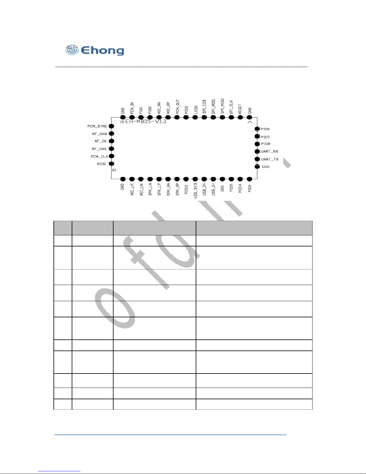
5. Pinout and Terminal Description
5.1. Pin assignment
Figure 1:
Pinout of EH
-
MB05
Pin Symbol I/O Type Description
1 GND Ground Ground
Active LOW RESETB, input debounced
so must be low for >5ms to cause a
RESETB
CMOS input with weak
internal pull-up
2 RESETB
Input with weak internal pull- Serial Peripheral interface clock for
3
4
5
SPI_CLK
SPI_MISO
SPI_MOSI
down programming only
CMOS output, tri-state, with
weak internal pull
-down
Serial Peripheral Interface output for
programming only
CMOS input, with weak
internal pull-down
Serial Peripheral Interface input for
programming only
Chip select for Synchronous Serial
Interface for programming only, active
low
Input with weak internal pullup
6
7
8
SPI_CSB
LED0
Open drain output LED Driver
Bi-directional with
programmable strength
PIO3 Programmable input/output line
internal pull-up/down
CMOS output, tri-state, with
weak internal pull
-down
9 PCM_OUT
Synchronous Data Output
10
11
MIC_RP
MIC_RN
Analogue
Analogue
Microphone input positive, right
Microphone input negative, right
Shanghai Ehong Technologies Inc
 Loading...