

Page 1
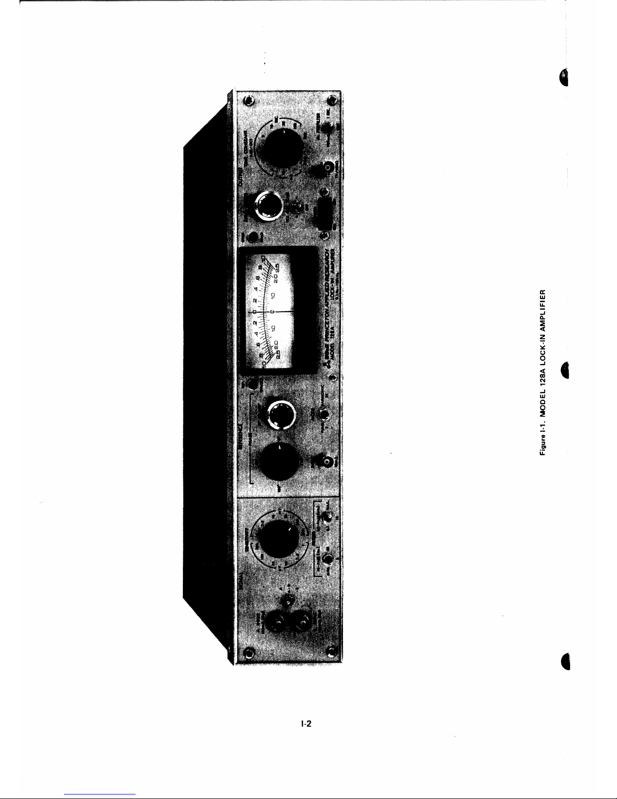
MODEL
128A
LOCK-IN
AMPLIFIER
SEE SAFETY NOTICE
PRECEDNG SECTION I
;EFORE OPERATING INSTRUMENT
OPERATING
AND
SERVICE
MANUAL
Page 2
M128A; 9/83·500·MIC
MODEL
128A
LOCK-IN
AMPLIFIER
OPERATING
AND
SERVICE
MANUAL
n
~~
G
BROOKDEAL
ELECTRONICS
~~
.:;;;;;~I:..
PRINCETON
APPL/ED
RESEARCH
Copyright
© 1983 EG&G PRINCETON APPLIED RESEARCH
Printed
In U.S.A.
Page 3
SHOULD YOUR EQUIPMENT REQUIRE SERVICE
A. Contact the factory
(6091452-2111)oryour
local factory
representative to discuss the problem. In many cases it
will be possible to expedite servicing by localizing the
problem to a particular plug-in
circuit
board.
B. If it is necessary to send any equipment back to the fac-
tory, we need the following information.
(1) Model number and serial number.
(2) Your name (instrument user).
(3) Your address.
(4) Address to
which
instrument should be returned.
(5) Your telephone number and extension.
(6) Symptoms (in detail,
including
control
settings).
(7) Your purchase order number for repair charges (does
not apply to repairs in warranty).
(8) Shipping
instructions
(if you wish to authorize ship-
ment by any method
other
than normal surface
transportation).
C. U.S. CUSTOMERS-·-Ship the equipment being returned
to:
EG&G PRINCETON APPLIED RESEARCH
7 Roszel Road
(Off Alexander Road, East of Route 1)
Princeton, New Jersey
D. CUSTOMERS OUTSIDE OF
U.S.A.-To
avoid delay in
customs clearance of equipment being returned, please
contact the factory or the nearest factory
distributor
for
complete shipping information.
E. Address correspondence to:
EG&G PRINCETON APPLIED RESEARCH
P. O. Box 2565
Princeton, NJ 08540
Phone:
6091452-2111
TELEX: 84 3409
WARRANTY
EG&G PRINCETON APPLIED RESEARCH warrants each instrument of
its
manufacture to be free from defects in material
and workmanship. Obligations under
this
Warranty shall be
limited
to replacing, repairing or giving credit for the purchase
price, at our option, of any instrument returned, freight
prepaid, to our factory
within
ONE year of delivery to the
original purchaser, provided
prior
authorization for such return
has been given by our authorized representative.
This Warranty shall not apply to any instrument which our in-
spection shall
disclose
to our satisfaction, has become detective or unworkable due to abuse, mishandling, misuse, accident, alteration, negligence, improper installation or
other
causes beyond our control.
Instruments
manufactured by
others, and included in or supplied
with
our equipment, are not
covered by
this
Warranty but carry the original manufacturer's
warranty which is extended to our customers and may be more
restrictive. Certain subassemblies, accessories or
corn-
ponents may be specifically excluded from
this
Warranty, in
which case such exclusions are listed in the
Instruction
Manual supplied
with
each instrument.
We reserve the right to make changes in design at any time
without
incurring any obligation to install same on
units
previously purchased.
THERE ARE NO WARRANTIES WHICH EXTEND BEYOND THE
DESCRIPTION HEREIN. THIS WARRANTY IS IN LIEU OF, AND
EXCLUDES ANY AND ALL OTHER WARRANTIES OR REPRE·
SENTATIONS, EXPRESSED, IMPLIED OR STATUTORY, IN·
CLUDING MERCHANTABILITY AND FITNESS, AS WELL AS
ANY AND ALL OTHER OBLIGATIONS OR LIABILITIES OF
EG&G PRINCETON APPLIED RESEARCH, INCLUDING, BUT
NOT LIMITED TO, SPECIAL OR CONSEQUENTIAL DAMAGES.
NO PERSON, FIRM OR CORPORATION IS AUTHORIZED TO
ASSUME FOR EG&G PRINCETON APPLIED RESEARCH ANY
ADDITIONAL OBLIGATION OR LIABILITY NOT EXPRESSLY
PROVIDED FOR HEREIN EXCEPT IN WRITING DULY EXECUTED BY AN OFFICER OF EG&G PRINCETON APPLIED
RESEARCH.
Page 4
Section
II
III
IV
V
TABLE
OF CONTENTS
CONDENSED
OPERATING
INSTRUCTIONS
CHARACTER
ISTICS
2.1
Introduction
2.2 Specifications
INITIAL
CHECKS
3.1
Introduction
3.2 Equipment Needed
3.3 Procedure
OPERATING
INSTRUCTIONS
4.1
Introduction
4.2 Preliminary Considerations
4.2A
Power Requirements
4.2B Fusing
.....
4.2C Warm-Up Period
4.20
Operating Frequency
4.2E
Grounding...
4.2F Noise
.....
4.3 Operating the Model 128A
4.3A
Introduction..
4.3B Reference Channel
4.3C Signal Channel
4.30
Output
Channel Controls
4.4 Mixer
Function
and Harmonic Sensitivity
4.5 Interface Connector .
4.6 Battery Operation .
4.7 Operation
with
the Internal Reference Oscillator
4.7A
Introduction
4.7B Operation . . . . . . . . . . .
4.7C Installation .
4.8 Operation
with
the Internal Tuned
Amplifier
4.8A
Introduction
4.8B
Operation.........
4.8C Installation .
4.9 More Reference Channel Operating Hints
4.9A
Reference Channel Slewing Rate
4.9B
Phase
Errors
with
Small Reference Signals
ALIGNMENT
.
5.1
Introduction
5.2 Required Equipment
5.3 Preliminary Steps
5.4 Procedure
5.4A
+15 V
Adjust
(R310),
-15
V Check, and +5 V Check
5.4B Reference Board Adjustments
5.4C Signal Board
Adjustment
5.40
Mixer Adjustments
5.4E Other Adjustments
Page
1-1
11-1
11-1
11-1
111-1
111-1
111-1
111-1
IV-l
IV-l
IV-l
IV-l
IV-l
IV-l
IV-l
IV-l
IV-3
IV-5
IV-5
IV-5
IV-6
IV-8
IV-9
IV-10
IV-10
IV-l0
IV-10
IV-10
IV-ll
IV-12
IV-12
IV-13
IV-15
IV-15
IV-15
IV-15
vi
V-l
V-l
V-l
V-l
V-l
V-l
V-3
V-3
V-4
Page 5
VI
VII
Number
1·1
IV·l
IV-2
'V-3
IV-4
IV-5
IV·6
IV·7
IV-8
IV-9
IV-10
rvu
IV·12
IV-13
IV·14
IV·15
vi
Number
IV-l
.V-2
TROUBLESHOOTING
6.1 Introduction
6.2 Equipment Required
6.3 Initial Steps . . . .
6.4 Power Supply Checks
6.5
Reference Checks
6.6 Signal Channel Amplifiers
6.6A Preamplifier
6.6B Intermediate AC Amplifiers
6.6C Final AC Amplifier
6.7 Mixer
6.8 DC Amplifiers .
SCHEMATICS, Table of
FIGURES
Model 128A Lock-In Amplifier .
Ground-Loop Suppression by Ten-Ohm Input Ground
Differential Measurement of "Single-Ended" Signal
Differential Measurement of
"Off-Ground"
Signal
Example of Everything
"Done
Wrong"
Errors Depicted in Figure IV-4 Corrected
Typical Model
l28A
Noise Figure Contours
Pulse Train as Reference Drive
Net Phase
Shift
Between Signal and Reference Channels as a
Function
of Frequency
Amplitude and Phase Characteristics of Hi-Pass Filter
Amplitude and Phase Characteristics of Low-Pass Filter
Examples of
Output
Filter Interactions . . . . .
Mixer
Output
for In-Phase and Quadrature Signals
Internal Oscillator Board Installed . . . . . . .
Tuned Amplifier Installed .
Phase/Amplitude Characteristics of Tuned Amplifier
Model 128A Adjustments and
Testpoints
.....
TABLES
Interface Connector Pin Assignments
Frequency Range as a Function of Capacitors
ii
VI-'
VI-'
VI·'
VI-'
VI·'
VI-'
VI·2
VI-2
VI-2
VI-2
VI-2
VI-2
VII·'
Page
.
1-2
IV-l
IV-'
IV-2
IV-2
IV·3
IV·3
IV·5
IV-6
IV-7
IV-7
IV-8
IV-9
IV·12
IV·13
IV·14
. V·2
Page
IV·l0
IV·l1
Page 6

SAFETY CONSIDERATIONS
A. INTRODUCTION
The apparatus to
which
this
instruction
manual
applies has been supplied in a safe
condition.
This manual
contains
some
information
and warn-
ings that have to be
followed
by the user to ensure
safe operation and to retain the apparatus in a
safe condition. The described apparatus has been
designed
for
indoor
use.
B. INSPECTION
Newly received apparatus should be
inspected
for
shipping damage. If any is noted,
immediately
notify EG&G PARC and file a claim
with
the car-
rier. The shipping
container
should be saved
for
possible
inspection
by the carrier.
WARNING!
THE PROTECTIVE GROUNDING COULD BE
RENDERED INEFFECTIVE IN DAMAGED APPARATUS.
DAMAGED
APPARATUS
SHOULD NOT BE ·OPERATED UNTIL ITS
SAFETY HAS BEEN VERIFIED BY QUALIFIED SERVICE PERSONNEL. DAMAGED APPARATUS WAITING FOR SAFETY VERIFICATION SHOULD BE TAGGED TO INDICATED TO A POTENTIAL USER THAT IT
MAY BE UNSAFE AND THAT IT SHOULD
NOT BE OPERATED.
C. SAFETY MECHANISM
As defined in IEC Publication 348 (Safety Require-
ments
for
Electronic
Measuring
Apparatus), the
Model 128A is Class I apparatus, that is, apparatus
that depends on
connection
to a protective con-
ductor
to earth ground for
equipment
and operator
safety. Before any
other
connection
is made to the
apparatus, the protective earth terminal shall be
connected to a protective conductor. The protective connection is made via the earth ground
prong of the M128A's power cord plug. This plug
shall only be inserted
into
a socket
outlet
provided with the required earth ground contact. The
protective action
must
not be negated by the use
of an extension cord
without
a protective conduc-
tor, or by use of an
"adapter"
that
doesn't
main-
tain earth ground
continuity,
or by any
other
means.
The power cord plug provided is of the type illus-
trated in Figure 1. If
this
plug is
not
compatible
with the available power
SOCkets,
the plug or
power cord should be replaced
with
an approved
type of
compatible
design.
WARNING!
IF IT IS NECESSARY TO REPLACE THE
POWER CORD OR THE POWER CORD
PLUG, THE REPLACEM ENT CORD OR PLUG
MUST HAVE THE SAME POLARITY AS THE
ORIGINAL. OTHERWISE A SAFETY HAZARD
FROM
ELECTRICAL
SHOCK,
WHICH
COULD RESULT IN PERSONAL INJURY OR
DEATH, MIGHT RESULT.
L =
LINEORACTIVE
CONDUCTOR (ALSO CALLEU
"LlV£"OR"HOT")
N =
NEUTRALORIDENTIFIED
CONDUCTOH
E
=EARTH OR SAFETY GROUND
Figure 1. POWER CORD PLUG WITH POl.ARITY INDICATIONS
D. POWER VOLTAGE SELECTION AND
LINE FUSES
Before
plugging
in the
power
cord, make sure that
the
equipment
is set to the voltage of the ac
power
supply.
CAUTION!
THE APPARATUS DESCRIBED IN THIS
MANUAL
MAY BE DAMAGED IF IT IS SET
FOR OPERATION FROM 110 V AC AND
TURNED ON WITH 220 V AC APPLIED TO
THE POWER INPUT CONNECTOR.
A detailed
discussion
of how to
check
and.tt
nec-
essary, change the power-voltage
setting
follows.
The line voltage is selected by means of a rearpanel
switch.
FOR SAFETY, UNPLUG THE
POWER CORD WHEN CHECKING THE LINE
VOLTAGE SETTING OR WHEN CHECKING THE
FUSES. FUSES SHOULD ONLY BE CHANGED BY
QUALIFIED SERVICE PERSONNEL WHO ARE
AWARE OF THE HAZARDS INVOLVED. Depending on the
switch
position,
either
"115"or"230"
(both are printed on the
swltchj-wl!lbevisible
to
the viewer. For operation from a line voltage from
100 V ac to 130 V ac, 50-60 Hz,
"115"
should
show.
Page 7
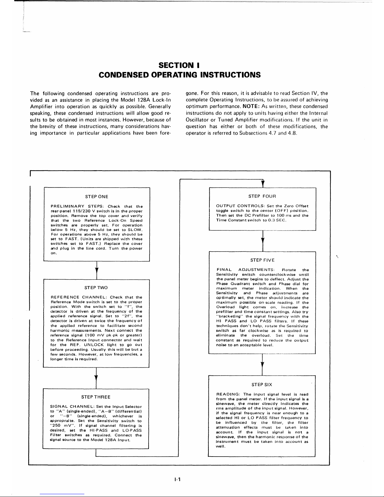
SECTION I
CONDENSED OPERATING INSTRUCTIONS
The
following
condensed
operating
instructions
are pro-
vided as an assistance in placing
the
Model
128A
Lock-In
Amplifier
into
operationasquickly
as possible.
Generally
speaking,
these
condensed
instructions
will
allow
good
re-
sults
to be
obtainedinmost
instances.
However,
because
of
the
brevity of
these
instructions,
many
considerations
hav-
ing
importanceinparticular
applications
have
been
fore-
STEP ONE
PRELIMINARY
STEPS;
Check
that
the
rear-panel
115/230Vswitch
is in
the
proper
position.
Remove
the
top
cover
and
verify
that
the
two
Reference
Lock-On
Speed
switches
are
properly
set.
For
operation
below5Hz,
they
shouldbesettoSLOW.
For
operations
above5Hz,
they
should
be
settoFAST.
(Units
are
shipped
with
these
switches
settoFAST.)
Replace
the
cover
and
pluginthe
line
cord.
Turn
the
power
on.
STEP TWO
REFERENCE
CHANNEL:
Check
that
the
Reference
Mode
switchissettothe
proper
position.
With
the
switch
setto"f",
the
detectorisdrivenatthe
frequencyofthe
applied
reference
signal.
Setto"2f",
the
detectorisdrivenattwice
the
frequency
of
the
applied
reference
to
facilitate
second
harmonic
measurements.
Next
connect
the
reference
signal
(100
m V pk -pkorgreater)
to
the
Reference
Input
connector
and
wait
for
the
REF.
UNLOCK
lighttogo
out
before
proceeding.
Usually
this
willbebut
a
few
seconds.
However,atlow
frequencies,
a
longer
timeisrequired.
STEP
THREE
SIGNAL
CHANNEL:Set
the
Input
Selector
to
"A"
(single-ended),
"A-B"
(differential)
or
"-B"
(single-ended),
whichever
is
appropraite.
Set
the
Sensitivity
switch
to
"250
mV".
If
signal
channel
filtering
is
desired,
set
the
HI-PASS
and
LO-PASS
Filter
switches
as
required.
Connect
the
signal
sourcetothe
Model
128A
Input.
1-1
gone.
For
this
reason,
it is advisabletoread
Section
IV,
the
complete
Operating
Instructions,tobe
assured
of achieving
optimum
performance.
NOTE:Aswritten,
these
condensed
instructionsdonot
applytounits
having
either
the
Internal
OscillatororTuned
Amplifier
modifications.Ifthe
unit
in
question
has
eitherorbothofthese
modifications,
the
operatorisreferredtoSubsections
4.7
and
4.8.
STEP
FOUR
OUTPUT
CONTROLS;
Set
the
Zero
Offset
toggle
switchtothe
center
(OFF)
position.
Then
set
theDCPrefilterto100msand
the
Time
Constant
switchto0.3
SEC.
STEP
FIVE
FINAL
ADJUSTMENTS:
Rotate
the
Sensitivity
switch
counterclockwise
until
the
panel
meter
beginstodeflect.
Adjust
the
Phase
Quadrant
switch
and
Phase
dial
for
maximum
meter
indication.
When
the
Sensitivity
and
Phase
adjustments
are
optimally
set,
the
meter
should
indicate
the
maximum
possible
on-scale
reading.Ifthe
Overload
light
comes
on,
increase
the
prefilter
and
time
constant
settings.
Also
try
"bracketing"
the
signal
frequency
with
the
HI
PASS
and
LO
PASS
filters.Ifthese
techniques
don't
help,
rotate
the
Sensitivity
switchasfar
clockwise
as is
required
to
eliminate
the
overload.
Set
the
time
constant
as
requiredtoreduce
the
output
noisetoan
acceptable
level.
STEP SIX
READING:
The
input
signal
levelisread
from
the
panel
meter.Ifthe
input
signal
is a
sinewave,
the
meter
directly
indicates
the
rms
amplitudeofthe
input
signal.
However,
if
the
signal
frequencyisnear
enoughtoa
selectedHIorLOPASS
filter
frequency
to
be
influenced
by
the
filter,
the
filter
attenuation
effects
must
be
taken
into
account.
If
the
input
signalisnot
a
sinewave,
then
the
harmonic
responseofthe
instrument
mustbetaken
into
account
as
well.
Page 8
1-2
a:
w
u.
-'
Q.
~
~
~
c
0
t
-'
~
co
N
...
-'
W
0
i
...
e
::l
'"
u::
Page 9

SECTION
II
CHARACTERISTICS
2.1 INTRODUCTION
The
Model
128A
Lock-In
Amplifier
enables
the
accurate
measurementofsignals
contaminatedbybroad-band
noise,
power
line
pickup,
frequency
drift,orother
sources
of
interference. It
does
thisbymeans
of an
extremely
narrow
band
detector
which
has
the
centerofits
passband
locked
to
the
frequencyofthe
signaltobe
measured.
Because
of
the
frequency
lock
and
narrow
bandwidth,
large
improvements
in signal-to-noise
ratio
can
be achieved,
allowing
the
signalofinteresttobe
accurately
measured,
even in
situations
where
it is
completely
masked
by noise.
Signals applied
to
the
input
(single-ended or
differential)
1
routed
through
a series of amplifiers
which
allow
..rll-scale sensitivity ranges
downtoone
microvolt.
Switch
selectable low-pass
and
high-pass filters allow
considerable
noise
reduction
aheadofthe
phase-sensitive
detector.
This
pre-detector
noise
reduction
canbefurther
enhanced
by
making
use of
the
optional
plug-in (internal) selective
amplifier. At
the
phase
sensitive
detector,
the
signal is
compared
with
the
reference
signal derived
from
the
experiment.
Only
those
signal
components
which
are
synchronous
with
the
reference
yieldanetdcdetector
output.
Noise
and
other
non-synchronous
signalsdonot
contributeanetdcoutput,
but
onlyacfluctuations
which
canbereducedtoany
arbitrary
value
accordingtothe
amount
of filtering
selected
with
the
Time
Constant
switch.
This switch allows
time
constants
as large as
100
seconds
to
be
selected,
with
provision for achieving larger
externally
determined
time
constants
if necessary.
Post-detector
dc
amplifiers drive
the
panel
meter
and
signal
output
connectors.
Other
features
include
provision
for
calibrated
zero
suppression of up to10x full scale, a
two-position
dc
prefilter,
and
the
capability
of driving
the
reference
input
the
detector
at
double
the
frequency
of
the
signal
applied to
the
Reference
Input
connector
to
facilitate
second
harmonic
measurements.
An
optional
plug-in
oscillator
(internal)
is available for use in
applications
where
the
experiment
does
not
produceareference
signal itself,
but
is capableofbeing
driven
by a signal
furnishedbythe
Lock-In Amplifier.
With its wide range of capabilities
and
easeofoperation,
the
Model
128A
Lock-In
Amplifier
should
find
extensive
applicationinsituations
where
the
accurate
measurement
of signals is
complicated
by
the
presenceofnoise and
interference.
2.2 SPECIFICATIONS
SIGNAL
CHANNEL
(1) INPUT
TYPE
Single-endedordifferentialasselectedbyfront-panel
switch.
11-'
(2)
INPUT
IMPEDANCE
100
Mr2
shuntedbyno
more
than20pF.
(3)
SENSITIVITY
12 full-scale ranges in
1-2.5-10
sequence
from1J.1V
to
250
mV.
(4) FREClUENCY
RANGE
0.5Hzto
100
kHz.
(5) COMMON MODE
REJECTION
At least
100dBat
1 kHz.
(6) MAXIMUM COMMON MODE
VOLTAGE
3 V
pk-pkto20
kHz;
then
--6
dB/octave
above
20
kHz.
(7)
DETECTOR
BIAS
Internal
network
allows dc bias
current
of
either
polaritytobe
providedatthe
"A"
Inputtofacilitate
operation
with
diode
detectors
which
require
biasing.
(See page VII-3
and
Parts
Location
Diagramonpage
VII-2.)
(8) NOISE
At 1 kHz
the
signal
channel
noise will
not
exceed
10
nV/H
zY2.
(9) LOW PASS
FILTER
Switch
selectable6dB/octave
low-pass filter
which
can be
set
to 3 dB
down
frequenciesof100
Hz,
10
kHz, or MAX
(greater
than
100
kHz).
(10)
HIGH PASS
FILTER
Switch
selectable6dB/octave
high-pass filter
which
can be
setto3 dB
down
frequenciesof50
Hz, 5 Hz,
or MIN
(below
0.5
Hz).
(11)
OVERLOAD
DETECT
Front-panel
indicator
lights if
applied
signal plus noise
is large
enoughtocause
overloadatany
of several
critical
overload
monitor
points.
(12)
GAIN
STABILITY
Page 10
(13) GAIN
LINEARITY
0.05%.
(14)
OVERALL
GAIN ACCURACY
±2%.
REFERENCE
CHANNEL
The
Model
128A
reference channel
automatically
locks
onto
and
tracksanapplied
reference signal over the
entire
operating
frequency
range of
the
instrument.
As a result,
the
instrumentisimmunetofrequency
and phase
shifts
as
long as
the
reference and signal to be recovered change
together.
(1)
TRACKING
RANGE
5 Hz to
100
kHz (FAST) or
0.5
Hz to
100
kHz
(SLOW) as
determinedbythe
settingoftwo
internal
switches.
Faster
lock-on
time
and slewing
rate
obtained
with
switches
settoFAST
make
this range
preferable
except
when
operating
below 5 Hz.
(2) MODES
Eitheroftwo
modes, f and 2f, can be selected by
means of a front-panel switch. In
the
"f"
position,
the
phase-sensitive
detector
is driven at
the
same
frequencyasthe
applied reference signal. In
the
"2f"
position,
the
phase-sensitive
detector
is driven at twice
the
frequency
of
the applied reference signal
to
facilitate
second
harmonic
measurements.
(3) INPUT IMPEDANCE
10
Mrl
shuntedbyno
more
than20pF.
(4) MINIMUM
REFERENCE
SIGNAL
REQUIREMENT
100
mV pk-pk,
any
waveshape crossing its
mean
only
twice each cycle. Minimum
time
required on
either
sideofthe
meanis100
ns.
Amplitude
excursions
must
be at least50mV on each sideofthe
mean.
Maximum
input
signal is 5 V (pk-to-rnean}. Best phase
accuracy
is
obtained
with
a 1 V rms sinewave.
(5) LOCK-ON TIME
A
function
of internal
switch
setting
as follows.
Selected
Range Lock-On
Time
SLOW (0.5 Hz to
100
kHz)
20
sec. per
octave
FAST (5 Hz to
100
kHz) 2 sec. per octave
(6) PHASE
Calibrated Phase
controls
allow the phase of
the
reference drive to
the
Phase-Sensitive
Detector
to be
set at any angle relative to
the
input
signal.
The
controls
consist of a Phase Dial with a range of
100°
and a Phase
Quadrant
switch
which
provides
incremental phase shifts of
90°.
The
phase
shift
11-2
accuracy of
the
dial is
better
than
0.2
0
over the
entire
frequency
range.
The
resolutionofthe
dial is
better
than
0.10.The
incremental
phase shiffs provided by
the
Quadrant
switch are
accurateto0.2°.
The
overall
phase accuracy of
the
instrument,
including
shifts
in
both
the reference and signal channels, is typically
better
than
50.
(7)
DETECTOR
BIAS
Internal
network
allows de bias
currentofeither
polarity
to be provided at
the
REF.INconnector
to
facilitate
operationinsituations
where
the
reference
signal is
taken
from
diodes requiring biasing. (See page
VII-6 and Parts Location Diagram
on
page VII-5.)
PHASE
SENSITIVE
DETECTOR,DCAMPLIFIER
(1)
OUTPUT
DRIFT
(2)
OVERLOAD
CAPABILITY
1000
times full scale up to a
maximumatthe
input
of
650
mV rms. Overload capability is
definedasthe
ratio, at
the
input
of the Model
128A,
of
the
maximum
pk-pk
non-coherent
signal
which
can be
applied
without
overloading the Model
128Atothe
pk-pk
coherent
signal required to yield full scale
Model
128A
output.
Note
that,
expressed as
the
ratio
of
the
pk-pk
non-coherent
signaltothe
rms value of
the
coherent
signal
required
for full-scale
output,
this
number
can be as
greatas2800.
Maximum
acceptable
signal is a
650
mV rms sinewave.
(3)
NON-COHERENT
REJECTION
50
ppm
maximum.
Non-coherent
rejection is
defined
as
that
offset
which
results
from
applying a
non-coherent
signal having a
pk-pk
amplitude
1000
times
the
pk-pk
amplitude
of
the
coherent
signal
requiredtoobtain
full-scale
output.
Example: With a
non-coherent
signal applied having a
pk-pk
amplitude
1000
times
the
pk-pk
coherent
signal
required
to
obtain
full-scale
output,
there
will
occur
an
offsetatthe
output
caused by
the
non-coherent
input
signal.
The
amplitude
of this
offset
will be no
greater
than:
50 X
10-
6
X
1000
= 50 X
10-3of f.s.
output
=50 mV (f.s. =1 V)
(4) TIME
CONSTANT
Front-panel switch allows selection of 6
dB/octave
filter
time
constants
of 1 ms, 10 ms, and .1 s
through
100
s in 1-3-10 sequence. Also MIN (time
constant
:::=0.7
ms) and EXT, which allows
time
constants
longer
than
100
s to be achieved by means of
external
Page 11
capacitors. A
separate
front-panel
toggle switch allows
another6dB/octave
filter to be
inserted,
if desired.
This filter has a
time
constantofeither
100
ms or 1 s,
whichever is selected.
(5)
ZERO
OFFSET
A
calibrated,
ten-turn,
Zero
Offset
dial,
with
up to
ten
times full-scale
capability
is provided.
(6) FULL-SCALE
OUTPUT
±1 V.
(7)
OUTPUTS
(a) Panel
meter,
± full scale.
(b)
Front-panel
BNC
connector.
One volt
out
corresponds
to full-scale panel
meter
deflection.
Output
resistance is
600
ohms.
(c) Rear-panel
Recorder
Out
binding posts,
spaced
to
accept
standard
double-banana
connector.
Output
resistance is
600
ohms.
GENERAL
(1) AMBIENT
OPERATING
TEMPERATURE
RANGE
(2)
AUXILIARY
POWER
OUTPUT
±15.5
V regulated dc
at
20 mA is
provided
at
rear-panel
connector.
(3) POWER
REQUIREMENTS
100-130
V ac
or
200-260
V ac,
50-60
Hz. May also be
powered
from
±24 V de
source
(such as
batteries).
Power
consumption:15watts.
(4) SIZE
17-3/4"
W x
3-1/2"
H x
14"D(45cmW x 9 cm H x
36 cm D).
11-3
(5)
WEIGHT
14 Ibs
(6.4
kg).
(6)
MODIFICATIONS
(a) Model
128A/97
Monitor
Modification
Three
rear-panel BNC
connectors
are installed
which
permit
monitoring
of:
(1)
OutputofSignal
Channel
before
demodulation
(please
note
that
the
Signal Channel
monitor
is provided as
part
of
the
Tuned
Amplifier
modification
as well), (2)
Squarewave
output
of Reference
Channel,
and
(3) Full-wave
demodulated
Mixer
output
before
Time
Constant
filter.
(b) Model
128A/98
Tuned
Amplifier Modification
Internal plug-in
board
is available
which
provides
a
tuned
bandpassornotch
characteristic
at a
Q-of-5.
The
frequency
can be
adjusted
over a 3: 1
range by
meansofa rear-panel
adjustment,
and
can be
settoany
frequency
from
1 Hz to
100
kHz by changing
capacitors
mounted
on
component
clips
located
on
the plug-in
circuit
board.
(c) Model
128A/99Internal
Oscillator
Modification
An internal low
distortion
oscillator
is available
which
provides a sinewave
output
adjustable
from
0-to-l0
V pk-pk
at
600
ohms.
The
frequencyisadjustable
over
about
a 3: 1 range by
means of a rear-panel
adjustment,
with
the
actual
frequency
range
spannedbythe
adjustment
being
determined
by a pair of
internal
capacitors
mounted
on
the
oscillator
circuit
board.
Operation
from
about
1 Hz
to
100
kHz is
possible. This
option,inconjunction
with
the
2f
mode
of
operation,
is
particularly
useful for
harmonic
detection
where
the
modulation
frequency
must
be at
one
half
the
detected
frequency.
Page 12
SECTION
III
INITIAL
CHECKS
3.1 INTRODUCTION
The
following
procedureisprovided
to facilitate initial
performance
checkingofthe
Model 128A. In general, this
procedure
should
be
performed
after
inspecting
the
instrument
for
shipping
damage
(any
notedtobe
reported
to
the
carrier
and
to
Princeton
Applied
Research
Corporation),
but
before
using
the
instrument
for
experimental
measurements.
Should
any
difficulty
be
encountered
in carrying
out
these checks,
contact
the
factoryoroneofits representatives. It
mightbenoted
that
it is
not
the
purpose
of these
checkstodemonstrate
that
the
instrument
meets
all specifications,
but
rather
simply
to
show
that
it is
functioning
normally.
If normal
indications
e
obtained
for
the
functions
checked,
one
may
reasonably
assume
that
those
functions
which
are
not
checked
are
working
properly
as well.
3.2 EQUIPMENT NEEDED
(1) Sinewave Oscillator
to
providea100
mV rms sinewave
at 1 kHz.
NOTE:Ifthe
instrumenttobe
checked
is
equipped
with
the
Tuned
Amplifier
modification,
then
the
oscillator
will have
to
provide a
100
mV rms
sinewave at
the
tuned
frequency.Ifthe
instrument
in
questionisequipped
with
the
Internal Oscillator
modification,noexternal
oscillator will be
required.
Th is applies
whetherornot
the
unitisequipped
with
the
Tuned
Amplifier
modification.
(2) General
purpose
oscilloscope. This
itemisrequired
only in
the
caseofunits
having
the
Tuned
Amplifier
modification.
'3) Suitable cables
for
interconnecting
the
above instru-
ments.
3.3 PROCEDURE
(1) Check
the
positionofthe
rear-panel
115/230
switch.
Be sure
the
number
showinginthe
window
corre-
spondstothe
line voltagetobe used.
(2) With the Power switch
settoOFF,
plug in
the
line
cord.
(3)
Set
the
Model
128A
controls
as follows.
Input
Selector: A
Sensitivity:
100
mV
Filters
HI-PASS: MIN.
LO-PASS: MAX.
Phase
Quadrant
switch:
270°
Phase dial:
90°
Mode: f
Zero
Offset
switch:
OFF
(center
position)
111·1
dial:
1.00
(one
turn
from
fully
counterclockwise
position)
Time
Constant:
.3 SEC.
DC Prefilter:
OUT
Reference
Tracking-Rate
switches
(two
internal
switches);
FAST
(unless
unitisequipped
with
Tuned
Amplifier'
or Internal Oscillator set for
frequency
below
5 Hz, in
which
case
switches
shouldbeset
to SLOW). NOTE:
Instruments
are
normally
shipped
with
these
switches set
to
FAST.
Power.
ON
(4) Applies
onlytounits
not
equipped
with
the
Internal
Oscillator
modification.Ifthe
Model
128A
has this
modification,goto
step
5.
Connect
the
outputofthe
external
oscillator
(set for
100
mV rms sinewave
out
at 1 kHz)toboth
the
"A"
and
Reference
Inputs. If
the
unitinquestion
has
the
Tuned
Amplifier
modification,
set
the
oscillatortothe
tuned
frequency
specified
when
the
unit
was
ordered.
(5) Applies
onlytounits
having
the
Internal Oscillator
modification.
Connectacable
from
the
rear-panel
REF.
OSC.
OUT
connectortothe
front-panel
"A"
Input.
There
is no
needtoconnect
th is signal to
the
Reference
Input
connector
(labeled MONITOR in
units
equipped
with
the
Oscillator
modification).
The
connectiontothe
Reference
Channel of
the
Model
128Aismade
internallyatthe
factory.
The
rear-panel
REF.
AM-
PLITUDE
adjustment
should
be
set
so
that
the
amplitude
of
the
signal at
the
REF.
OSC.
OUT
connectoris100
mV rms. An
accurateacvoltmeter
may be useful
for
setting
this
level (units leave the
factory
set
foranominal
100
mV rrns
out).
(6) Applies
onlytounits
having
the
Tuned
Amplifier
modification.
In
the
case
of
units
not
having
this
modification,
go d irectl ytostep
7.
(a)
Connect
the
oscilloscope to
the
rear-panel SIG.
MON.
connector.
(b)
Vary
the
frequencyofthe
signal applied to
the
"A"
Input
(use
the
rear-panel
REF.
OSC.
FREQ.
ADJ.
controlinunits
equipped
with
an Internal
Oscillator)
for
peak
signal
amplitude
as observed
with
the
oscilloscope.
(7)
Set
the
Phase
Quadrant
switchto0°.
Then
adjust
the
Phase dial
for
"0"
panel
meter
indication.
(8)
Set
the
Phase
Quadrant
switch
backto270°.
The
panel
meter
should
indicate
full scale to
the
right ± a
few
percent
of full scale.
The
accuracyofth is readinq
Page 13
will
depend
on the
amplitude
accuracy of the signal
applied
to
the
"A"
Input.
(9)
Adjust
the
amplitudeofthe
signal applied to
the
"A"
Input
as required to
obtain
exactly
full-scale panel
meter
indication.
(10)
Set
the
Phase
Quadrant
switch to
180°.
The
panel
meter
should
indicate
"0"
±5%offull scale.
(11)
Set
the
Phase
Quadrant
switchto90°.
The
panel
meter
should
indicate
negative full scale ±5% of full
scale.
(12)
Set
the
Phase
Quadrant
switch to
270°
to restore
the
111-2
positive full-scale panel
meter
indication.
(13)
Set
the
Zero
Offset
toggle switch to "+".
The
panel
meter
indication
should
go to
"0"
±5% of full scale.
(14) Begin
rotating
the
Offset
dial
counterclockwise.
The
panel
meter
indication
should
increase linearly, track-
ing
the
dial setting. When
the
dial is fully
counter-
clockwise,
the
panel
meter
should
indicate full scale
±5%. Reset
the
Zero
Offset toggle switch to
the
center
(OFF)
position.
This
completes
the
initial checks. If
the
indicated results
were
obtained,
one
can be reasonably sure
that
the Model
128Aisfunctioning
normally.
Page 14

SECTION
IV
OPERATING
INSTRUCTIONS
4.1 INTRODUCTION
Even
though
operation
of
the
Model
128Aisstraight-
forward,
there
are a
number
of
factorsofwhich
the
operator
should
be aware
to
be assured of achieving
optimum
performance
in all
situations.
This
sectionofthe
manual
treats
these
considerationsinsome
detail.
Topics
covered include
grounding,
noise
performance,
harmonic
sensitivity,
operation
in
conjunction
with
the
plug-in
accessories,
and
others.
For
an overall
"quick
look"athow
the
instrumentisoperated,
the
operatorisreferred
to
SectionI,the
condensed
operating
instructions.
4.2
PRELIMINARY
CONSIDERATIONS
4.2A
POWER
REQUIREMENTS
The
Model
128A
requires
100-130
V acor200-260
V ac,
50-60
Hz.
The
power
consumptionis15
watts.
The
unit
may also be
poweredbybatteriesbyapplying
±24 Vtothe
appropriate
pinsofthe
rear-panel octal-
connector
(see
BATTERY
OPERATION,
page
IV-l0).
A rear-panel slide
switch
determines
whether
the
ac
power
circuits
are
connected
for
operation
from
100-130
V or
from
200·260V.For
operation
from
100-130V,"115"
should
showinthe
window.
For
operation
from
200-260V,"230"
should
show.
4.28
FUSING
The
Model
128Aisprotected
by a single fuse
mounted
on
its rear panel. A
slow-blow
1/4
A fuse is used for
operation
from
115
V. A slow-blow
1/10
A fuse is used for
operation
from
230
V.Itoccasionally
happens
thataslow-blow
fuse
fails in
shipment
as a
resultofshock
and
vibration.
Hence,
if
the
fuse is
found
to be bad
when
the
instrument
is
operated
for
the
first
time
it is advisable to
try
and
change
the
fuse. If
normal
operation
follows,
chances
are
there
are
no
other
problems.
However, if
the
replacement
fuse fails,
thereissomething
wrong
which
will have to be
corrected
before
proceeding.
4.2C
WARM-UP
PERIOD
For
most
applications,
five
minutes.
Where it is
desired
to
achieve
the
best
possible gain
and
output
stability,
allow an
hour.
4.20
OPERATING
FREQUENCY
Although
one
can,
in principle,
make
equally
accurate
measurements
at any
frequency
within
the
operating
range
of
the
instrument,
operationissimplest
and
least
subject
to
error
over a range having as its
lower
limit,
perhaps
a few
hundred
Hz,
and
as its
upper,
perhaps
10k
Hz.Atvery low
frequencies,
phase
offsets
occur
which
could
matterifone
is
interestedinthe
absolute
phase of
the
input
signal.
Another
problemoflow
frequency
operationisthatofl/f
noise, including
both
that
which
developsinthe
Model
128A
and
that
which
originatesinthe
experiment
itself
to
degrade
the
signal-to-noise
ratio
ahead
of
the
lock-in
amplifier. Increased
response
and
settling
time
could
be a
IV-1
significant
problemifone
were
operatinginconjunction
with
the
optional
plug-in
tuned
amplifier.
At high fre-
quencies,
radiation
and
associated
pick-up
tend
to
be
bothersome.
Another
high
frequency
problemisthat
of
signal
attenuation
as a resultofthe
input
cable
capacitance.
Th is is especially a
problem
when
working
from
a high
source
resistance.
Other
frequencies
to avoid are60Hz
and
its
lower
order
harmonics.
By avoiding
these
frequencies,
the
operator
assures
that
he will be
measuring
the
signal
of
interest
only,
uninfluenced
by
power
frequency
pick-up,
either
internalorexternal.
4.2E
GROUNDING
In
any
system
processing low-level signals,
proper
grounding
to
minimize
the
effectsofground
loop
currents,
usually
at
the
power
frequency,
is an
important
consideration.Inthe
case of
the
Model
128A,
special design
techniques
have
been
employedtogive a high
degreeofground-loop
signal
rejectioninsingle-ended
applications.
Even so, it will
often
prove advisable to
operate
differentiallv.
even
when
ex-
amining
a single-ended signal
source,
10 achieve
the
greatest
possible
rejection.
Figures IV-l
and
IV-2
illustrate
this
point.
Note
from
Figure IV-l
that
the
signal
source
is
located
inside a
grounded
enclosure
(shield), to
which
signal
source
commonisattachedatone
point.
The
braid of
the
/
'U
,
INDUCED emf
(DISTRIBUTED AROUND
LOOP)
RESISTANCE OF AC GROUND
PATH--J
Figure
IV·l.
GROUND·LOOP
SUPPRESSION
BY
TEN-OHM
INPUT
GROUND
SHIELD
l_
10"
L
INDUCE~.mf
'"
(CJSTRIBUTED AROUND LOOP) J
RESISTANCE OF AC GROUND PATH
Figure
IV-2.
DIFFERENTIAL
MEASUREMENT
OF
"SINGLE-ENDED"
SIGNAL
Page 15
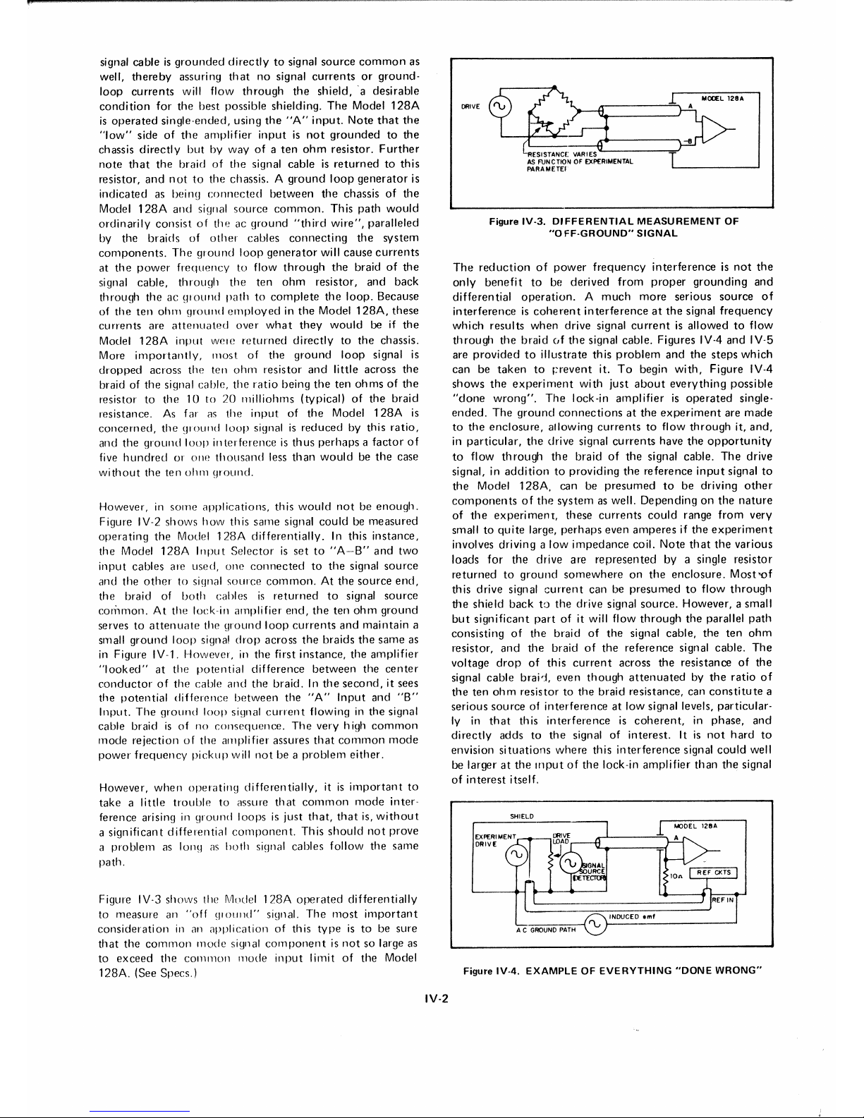
Figure
IV-4.
EXAMPLEOFEVERYTHING
"DONE
WRONG"
The
reductionofpower
frequency
interferenceisnot
the
only
benefit
to be
derived
from
proper
grounding
and
differential
operation.
A
much
more
serious
source
of
interferenceiscoherent
interferenceatthe
signal
frequency
which
results
when
drive signal
currentisallowedtoflow
through
the
braidofthe
signal
cable.
Figures IV-4
and
IV-5
are
providedtoillustrate
this
problem
and
the
steps
which
can
be
takentoprevent
it.
To
begin
with,
Figure
IVA
shows
the
experiment
with
just
about
everything
possible
"done
wrong".
The
lock-in
amplifierisoperated
single-
ended.
The
ground
connectionsatthe
experiment
are
made
to
the
enclosure,
allowing
currentstoflow
through
it,
and,
in
particular,
the
drive signal
currents
have
the
opportunity
to
flow th rough
the
braidofthe
signal cable.
The
drive
signal, in
additiontoproviding
the
reference
input
signal
to
the
Model
l28A,
can be
presumedtobe driving
other
componentsofthe
system
as well.
Dependingonthe
nature
of
the
experiment,
these
currents
could
range
from
very
small to
quite
large,
perhaps
even
amperesifthe
experiment
involves driving a
low
impedance
coil.
Note
that
the
various
loads
for
the
drive
are
represented
by a single
resistor
returnedtoground
somewhere
on
the
enclosure.
Most-of
this
drive
signal
current
canbepresumedtoflow
through
the
shield
backtothe
drive
signal
source.
However,
a small
but
significant
part
of it will
flow
through
the
parallel
path
consistingofthe
braidofthe
signal cable,
the ten
ohm
resistor,
and
the
braidofthe
reference
signal
cable.
The
voltage
dropofthis
current
across
the
resistanceofthe
signal
cable
brai-J,
even
though
attenuated
by
the
ratio
of
the
ten
ohm
resistortothe
braid
resistance, can
constitute
a
serious
sourceofinterference
at low signal levels,
particular-
ly in
that
this
interferenceiscoherent,
in
phase,
and
directly
addstothe
signal of
interest.
It is
not
hard
to
envision
situations
where
this
interference
signal
could
well
be larger at
the
Inputofthe
lock-in
amplifier
than
the
signal
of
interest
itself.
signal
cableisgrounded
directly
to signal
source
common
as
well,
thereby
assuring
that
no signal
currentsorground-
loop
currents
will
flow
through
the
shield,'adesirable
condition
for
the
best
possible
shielding.
The
Model
l28A
is
operated
single-ended,
using
the
"A"
input.
Note
that
the
"low"
side of
the
amplifier
inputisnot
groundedtothe
chassis
directly
butbywayofa
ten
ohm
resistor.
Further
note
that
the
braidofthe
signal
cableisreturnedtothis
resistor,
and
nottothe chassis. A
ground
loop
generator
is
indicatedasbeing
connected
between
the
chassis of
the
Model
l28A
and
siqnal
source
common.
This
path
would
ordinarily
consistoftheacground
"third
wire",
paralleled
by
the
braids
of
other
cables
connecting
the
system
components.
The
ground
loop
generator
will
cause
currents
at
the
power
frequencytoflow
through
the
braid of
the
signal cable,
through
the
ten
ohm
resistor,
and
back
through
theacwound
pathtocomplete
the
loop.
Because
of
the
ten
ohm
ground
employedinthe
Model
l28A,
these
currents
are
attenuated
over
what
they
would
be if
the
Model
128A
input
were
returned
directlytothe
chassis.
More
importantly,
most
of
the
ground
loop
signal is
dropped
across
the
ten
ohm
resistor
and
little
across
the
braid of
the
signal
cable,
the
ratio
being
the
ten
ohmsofthe
resistor to
the
10 to
20
milliohms
(typical)ofthe
braid
resistance, As far as
the
input
of
the
Model
l28A
is
concerned,
the
ground
loop
signal is
reduced
by this
ratio,
and
the
ground
loop
interferenceisthus
perhapsafactor
of
five
hundredorone
thousand
less
than
wouldbethe
case
without
the
ten
ohmqround.
However, in
some
appl
ications, th is
would
notbeenough.
Figure IV-2
shows
how
this
same
signal
couldbemeasured
operating
the
Model
128A
differentially.Inthis
instance,
the
Model
l28A
Input
Selectorissetto"A-B"
and
two
input
cables
are used,
one
connectedtothe
signal
source
and
the
other
to siqnal
source
common.Atthe
source
end,
the
braid
of
both
cables is
returned
to
signal
source
common.Atthe
lock-in
amplifier
end,
the
ten
ohm
ground
serves to
attenuate
the
wound
loop
currents
and
maintain
a
small
ground
loop
signa!
drop
across
the
braids
the
same
as
in Figure
IV-l.
However,inthe
first
instance,
the
amplifier
"looked"
at
the
potential
difference
between
the
center
conductorofthe
cable
and
the
braid.Inthe
second,
it sees
the
potential
difference
between
the
"A"
Input
and
"8"
Input.
The
ground
loop
siqnal
current
flowinginthe
signal
cable
braid is of no
consequence.
The
very high
common
mode
rejectionofthe
amplifier
assures
that
common
mode
power
frequency
pickup
will
not
be a
problem
either.
However,
when
operating
differentially,
it is
important
to
takealittle
trouble
to assure
that
common
mode
inter-
ference arising in
ground
loopsisjust
that,
that
is,
without
a
significant
differential
component.
This
should
not
prove
a
problemaslonqasboth
signal
cables
follow
the
same
path,
Figure IV-3
shows
the Model
128A
operated
differentially
to
measurean"off
~JI
ound
" siqn al.
The
most
important
consideration
in an
application
of this
type
is to be sure
that
the
common
mode
siqnal
componentisnot
so large as
to
exceed
the
common
mode
input
limitofthe Model
128A.
(See Specs.)
IV-2
DRIVE
~
~:£"
0'"''''''
,.0'"
-1
AS
FUNCTIONOFEXPERIMENTAL
PARAMETEI
L..-
...I
Figure
IV-3.
DIFFERENTIAL
MEASUREMENT
OF
"0
FF-GROUND"
SIGNAL
Page 16
DRIVE
LOAD
k =
Boltzmann's
constant=1.38x10-
2 3
joules/kelvin
T =
absolute
temperature
in kelvins
R
s
= Resistance in
ohmsofthe
resistive
component
of
the
impedance
across
which
the
voltage
iii
mea-
sured
B =
Bandwidth
over
which
the
measurementismade
Mathematically
expressed,
noise figure
canbestated
as:
NF(dB)
=
2010
9 10 Noise
V.olta~_~~g~!':l_~t
of
Amplifier
That
PortionofNumerator
Attributable
IV-2
to
Source
Thermal
Noise
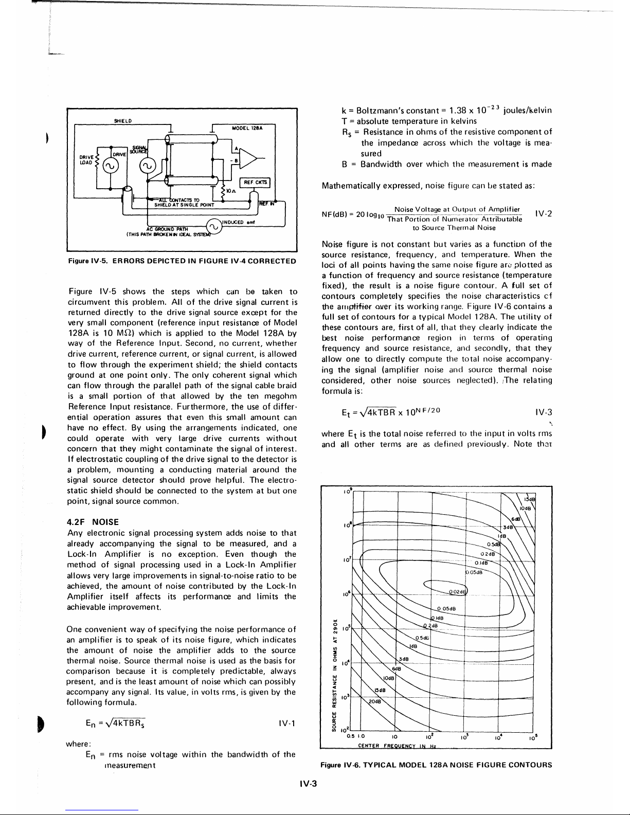
Figure IV-6.
TYPICAL
MODEL
128A
NOISE
FIGURE
CONTOURS
~~
where
Etis
the
total
noise
referredtothe
input
in volts rrns
and
all
other
terms
are as
defined
previously.
Note
thar
IV-3
10~
Et=V4kTBRX10NF/20
o
11>
N
~
Ul
2
:r
o
~
""
o
z
c(
Ii;
~
0:
""
U
~
~
102::-:~__~~---9:::'-'-_--.-l.-
__
.L,
__
--.J
0.5
10
CENTER fR
Noise figure is
not
constant
but
varies as a
functionofthe
source
resistance,
frequency,
and
temperature.
When
the
lociofall
points
having
the
same
noise figure are
plotted
as
a
functionoffrequency
and
source
resistance
(temperature
fixed),
the
result
is a noise figure
contour.
A full
set
of
contours
completely
specifies
the
noise
characteristics
cf
the
antpti#er
ruler its
working
range. Figure IV-6
contains
a
full
setofcontours
for a
typical
Model
128A.
The
utility
of
these
contours
are, first of all,
that
they
clearly
indicate
the
best
noise
performance
region in
terms
of
operating
frequency
and
source
resistance,
and
secondly,
that
they
allow
onetodirectly
compute
the
total
noise
accompany-
ing
the
signal
(amplifier
noise
and
source
thermal
noise
considered,
other
noise
sources
neglected).
.The
relating
formula
is:
IV-l
4.2F NOISE
Any
electronic
signal processing
system
adds
noise to
that
already
accompanying
the
signal to be
measured,
and
a
Lock-In
Amplifier
is no
exception.
Even
though
the
method
of signal processing
used
in a Lock-In
Amplifier
allows very large
improvements
in signal-to-noise
ratio
to be
achieved,
the
amount
of noise
contributedbythe
Lock-In
Amplifier itself
affects
its
performance
and
limits
the
achievable
improvement.
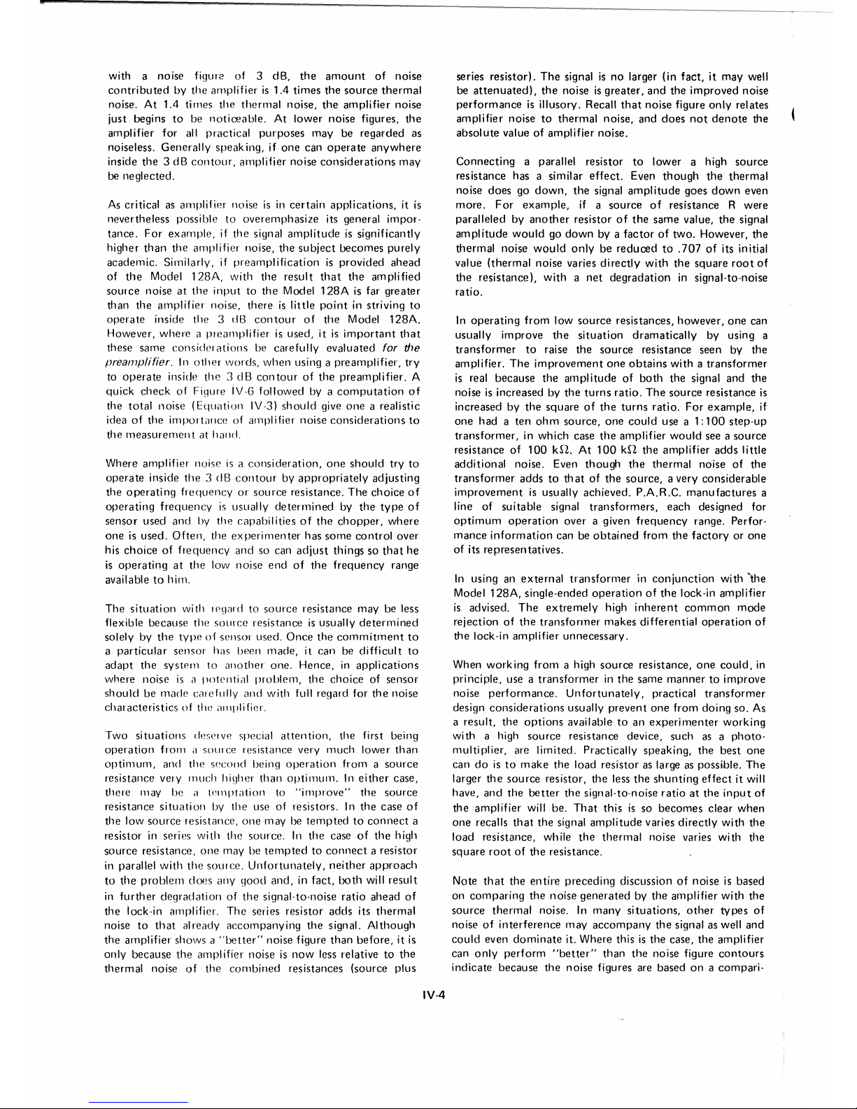
Figure IV-5
shows
the
steps
which
can be
taken
to
circumvent
this
problem.
Allofthe
drive signal
current
is
returned
directlytothe
drive signal
source
except
for
the
very small
component
(reference
input
resistance of Model
128A
is 10
MS1)
whichisappliedtothe
Model
128A
by
way of
the
Reference
Input.
Second,nocurrent,
whether
drive
current,
reference
current,
or signal
current,isallowed
to
flow
through
the
experiment
shield;
the
shield
contacts
groundatone
point
only.
The
only
coherent
signal
which
can
flow
through
the
parallel
pathofthe
signal cable braid
is a small
portionofthat
allowed by
the
ten
megohm
Reference
Input
resistance.
Furthermore,
the
use of
differ-
ential
operati
on assures
that
even th is small
amountcan
have no
effect.
By using
the
arrangements
indicated,
one
could
operate
with
very large drive
currents
without
concern
that
they
might
contaminate
the
signalofinterest.
If
electrostatic
couplingofthe
drive signaltothe
detector
is
a
problem,
mountingaconducting
material
around
the
signal
source
detector
should
prove
helpful.
The
electro-
static
shield
shouldbeconnectedtothe
systematbut
one
point,
signal
source
common.
Figure IV-5.
ERRORS
DEPICTEDINFIGURE
IV-4
CORRECTED
One
convenient
wayofspecifying
the
noise
performance
of
an
amplifieristo
speakofits
noise
figure,
which
indicates
the
amount
of noise
the
amplifier
adds
to
the
source
thermal
noise.
Source
thermal
noise is used as
the
basis for
comparison
because
it is
completely
predictable,
always
present,
andisthe
least
amount
of noise
which
can
possibly
accompany
any
signal. Its value, in volts rms, is given by
the
following
formula.
where:
En = rms noise voltage
within
the
bandwidthofthe
measurement
IV·3
Page 17
with
a noise figure of 3 dB,
the
amount
of
noise
contributedbythe
amplifier
is 1.4
times
the
source
thermal
noise.At1.4
times
the
thermal
noise,
the
amplifier
noise
just
beginstobe
noticeable.
At
lower
noise
figures,
the
amplifier
for
all
practical
purposes
mayberegarded
as
noiseless.
Generally
speaking,ifone
can
operate
anywhere
inside
the
3 dB
contour,
amplifier
noise
considerations
may
be
neglected.
As critical as
amplifier
noise is in
certain
applications,
it is
nevertheless
possibletooveremphasize
its general
impor-
tance.
For
example,ifthe
signal
amplitudeissignificantly
higher
than
the
amplifier
noise,
the
subject
becomes
purely
academic.
Similarly,ifpreamplificationisprovided
ahead
of
the
Model
128A,
with
the
result
that
the
amplified
source
noise at
the
inputtothe
Model
128A
is far
greater
than
the
amplifier
noise,
thereislittle
point
in striving to
operate
inside
the
3 dB
contour
of
the
Model
128A.
However,
whereapreamplifierisused,
it is
important
that
these
same
considerations
be
carefully
evaluated
for
the
preamplifier.
In
other
words,
when
using a
preamplifier,
try
to
operate
inside
the
3 dB
contourofthe
preamplifier.
A
quick
check
of
Fiqure iV-G
followed
by a
computation
of
the
total
noise
(Equation
IV-3)
should
give
one
a realistic
idea of the
importanceofamplifier
noise
considerations
to
the
measurementathand.
Where
amplifier
noise is a
consideration,
one
should
try
to
operate
inside
the
3 dB
contourbyappropriately
adjusting
the
operating
frequencyorsource
resistance.
The
choice
of
operating
frequencyisusually
determined
by
the
type
of
sensor
used
andbythe
capabilitiesofthe
chopper,
where
oneisused.
Often,
the ex
perimenter
has
some
control
over
his
choiceoffrequency
and
so can
adjust
thingssothat
he
is
operatingatthe
low
noise
endofthe
frequency
range
available to
him.
The
situation
with regard to
source
resistance
may
be less
flexible
because
the
source
resistanceisusually
determined
solely by
the
typeofsensor
used.
Once
the
commitment
to
a
particular
sensor
has
been
made,
it can be
difficult
to
adapt
the
systemtoanother
one.
Hence, in
applications
where
noise is a
uotcntial
problem,
the
choiceofsensor
shouldbemade
carefully
and
with
full regard for
the
noise
characteristics
of the amnlifier.
Two
situations
deserve special
attention,
the
first being
operation
fromasource
resistance very
much
lower
than
optimum,
and the
second
being
operation
fromasource
resistance very
much
higher
than
optimum.Ineither
case,
there
may be a
temptation
to
"improve"
the
source
resistance
situation
by
the
use of resistors. In
the
case
of
the low
source
resistance,
one
maybetemptedtoconnect
a
resistor in series
with
the
source.Inthe
caseofthe
high
source
resistance,
one
may be
temptedtoconnectaresistor
in parallel
with
the
source.
Unfortunately,
neither
approach
to
the
problem
does
any
good
and,infact,
both
will
result
in
further
degradationofthe
signal-to-noise
ratio
ahead
of
the
lock-in
amplifier.
The
series
resistor
adds
its
thermal
noisetothat
already
accompanying
the
signal.
Although
the
amplifier
showsa"better"
noise figure
than
before,
it is
only
because
the
ampl ifier
noiseisnow
less relative to
the
thermal
noise
of
the
combined
resistances (source
plus
IV-4
series
resistor).
The
signal is no larger (in
fact,itmay
well
be
attenuated),
the
noise is
greater,
and
the
improved
noise
performance
is illusory. Recall
that
noise
figure
only
relates
amplifier
noisetothermal
noise, and
does
not
denote
the
absolute
valueofamplifier
noise.
Connecting
a parallel
resistor
to
lower
a high
source
resistance has a similar
effect.
Even
though
the
thermal
noise
doesgodown,
the
signal
amplitude
goes
down
even
more.
For
example,
if a
source
of
resistanceRwere
paralleledbyanother
resistorofthe
same
value,
the
signal
ampl
itude
wouldgodown
by a
factoroftwo.
However,
the
thermal
noise
would
onlybereducedto.707ofits initial
value
(thermal
noise
varies
directly
with
the
square
root
of
the
resistance),
withanet
degradation
in signal-to-noise
ratio.
In
operating
from
low
source
resistances,
however,
one
can
usually
improve
the
situation
dramatically
by using a
transformer
to
raise
the
source
resistance
seen
by
the
amplifier.
The
improvement
one
obtains
withatransformer
is real
because
the
amplitudeofboth
the
signal and
the
noise is
increasedbythe
turns
ratio.
The
source
resistance is
increased by
the
squareofthe
turns
ratio.
For
example,
if
one
hadaten
ohm
source,
one
could
use a 1:
100
step-up
transformer,inwhich
case
the
amplifier
would
see a
source
resistance of
100
kn.
At
100
kS1
the
amplifier
adds
little
additional
noise. Even
though
the
thermal
noiseofthe
transformer
addstoth at of
the
source,
a very
considerable
improvement
is usually
achieved.
P.A.R.C.
manufactures
a
line of
suitable
signal
transformers,
each
designed
for
optimum
operation
over
a given
frequency
range. Perfor-
mance
information
can be
obtained
from
the
factoryorone
of its
representatives.
In using an
external
transformerinconjunction
with
'the
Model
128A,
single-ended
operationofthe
lock-in
amplifier
is advised.
The
extremely
high
inherent
common
mode
rejectionofthe
transformer
makes
differential
operation
of
the
lock-in
amplifier
unnecessary.
When
working
from
a high
source
resistance,
one
could,
in
principle,
use a
transformerinthe
same
mannertoimprove
noise
performance.
Unfortunately,
practical
transformer
design
considerations
usually
prevent
one
from
doing
so. As
a
result,
the
options
availabletoan
experimenter
working
with
a high
source
resistance device,
such
as a
photo-
multiplier,
are
limited.
Practically
speaking,
the
best
one
candoistomake
the
load
resistor
as large as possible.
The
larger
the
source
resistor,
the
less
the
shunting
effect
it will
have,
and
the
better
the
signal-to-noise
ratioatthe
input
of
the
amplifier
will be.
That
this
is so
becomes
clear
when
one
recalls
that
the
signal
amplitude
varies
directly
with
the
load
resistance, while
the
thermal
noise varies
with
the
square
rootofthe
resistance.
Note
that
the
entire
preceding
discussionofnoise
is based
on
comparing
the
noise
generatedbythe
amplifier
with
the
source
thermal
noise. In
many
situations,
other
types
of
noiseofinterference
may
accompany
the
signal as well and
could
even
dominate
it.
Where
this is
the
case,
the
amplifier
can
only
perform
"better"
than
the
noise figure
contours
indicate
because
the
noise
figures are basedona cornpari-
Page 18
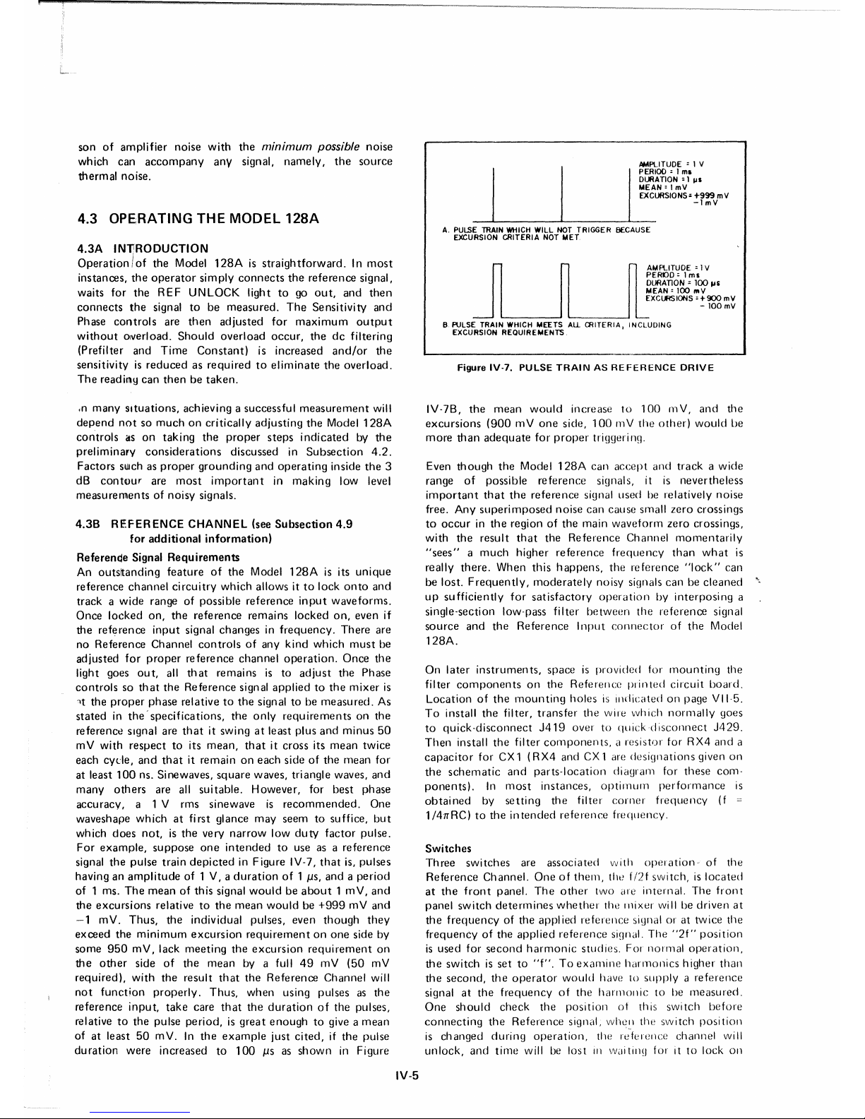
son of
amplifier
noise
with
the
minimum possible noise
which can
accompany
any
signal,
namely,
the
source
thermal
noise.
4.3 OPE;RATING THE MODEL
128A
4.3A
INliRODUCTION
Operation/of
the
Model
128Aisstraightforward.Inmost
instances,
the
operator
simply
connects
the
reference
signal,
waits
for
the
REF
UNLOCK
light to go
out,
and
then
connects
the
signal to be
measured.
The
Sensitivity
and
Phase
controls
are
then
adjusted
for
maximum
output
without
overload.
Should
overload
occur,
thedcfiltering
(Prefilter and
Time
Constant)
is
increased
and/or
the
sensitivity is
reducedasrequiredtoeliminate
the
overload.
The
readinq can
thenbetaken
.
•n
many
Situations,
achieving a successful
measurement
will
depend
notsomuchoncritically
adjusting
the
Model
128A
controlsason
taking
the
proper
steps
indicated
by
the
preliminary
considerations
discussed in
Subsection
4.2.
Factors
such as
proper
grounding
and
operating
inside
the
3
dB
contour
are
most
important
in
making
low level
measurementsofnoisy
signals.
4.38
REFERENCE
CHANNEL
(see
Subsection
4.9
for
additional
information)
Referende
Signal
Requirements
An outsltanding
featureofthe
Model
128A
is its
unique
reference
channel
circuitry
which
allows ittolock
onto
and
trackawide
range of possible
reference
input
waveforms.
Once
locked
on,
the
reference
remains
locked
on,
even if
the
reference
input
signal
changesinfrequency.
There
are
no
Reference
Channel
controlsofany
kind
which
must
be
adjusted
for
proper
reference
channel
operation.
Once
the
light goes
out,
all
that
remains
is to
adjust
the
Phase
controlssothat
the
Reference
signal
appliedtothe
mixer
is
-t
the
proper
phase
relativetothe
signal to be
measu
red. As
statedinthe'
specifications,
the
only
requirements
on the
reference signal are
that
it swing at least plus
and
minus
50
mV
with
respect
to its
mean,
thatitcross
its
mean
twice
each cycle,
and
thatitremainoneach
sideofthe
mean for
at least
100
ns. Sinewaves,
square
waves, triangle waves,
and
many
others
are all
suitable.
However,
for
best
phase
accuracy,
a 1 V rms sinewave is
recommended.
One
waveshape
whichatfirst
glance
may
seem
to suffice,
but
which
does
not,isthe
very
narrow
low
duty
factor
pulse.
For
example,
suppose
one
intended
to use as a
reference
signal
the
pulse
train
depicted
in Figure IV-7,
that
is, pulses
having an
amplitude
of 1 V, a
durationof1
JiS,
andaperiod
of 1 ms.
The
mean
of this signal
wouldbeabout1mV,
and
the
excursions
relativetothe
mean
wouldbe+999
mV
and
-1
mV.
Thus,
the
individual pulses, even
though
they
exceed
the
minimum
excursion
requirementonone
side by
some
950
mV,
lack
meeting
the
excursion
requirement
on
the
other
side
of
the
mean
by a full
49
mV
(50
mV
required),
with
the
result
that
the
Reference
Channel
will
not
function
properly.
Thus,
when
using pulses as
the
reference
input,
take
care
that
the
durationofthe pulses,
relative
to
the
pulse
period,isgreat
enough
to give a
mean
of at least50mV.Inthe
example
just
cited,
if the pulse
duration
were
increased to
100
JiS
as
shown
in Figure
IV-5
AMPLITUDE : 1 V
J
~
ERIOO
: 1
ml
DURATION:
1
III
MEAN:
I mV
'-
-'-_____
EXCURSIONS:
.!"f~vmv
A. PULSE TRAIN WHICH WILL NOT TRIGGER BECAUSE
EXCURSION CRITERIA NOT
MET
J
~
~
AMPLITUDE
: 1V
PEROO:
1ms
~tti~~~~
~~
liS
EXCURSIONS
:+900
mV
- 100 mV
-~
B PULSE TRAIN WHICH MEETS
All.
CRITERIA, INCLUDING
EXCURSION REQUIREMENTS
Figure
IV-7.
PULSE
TRAINASREFERENCE
DRIVE
IV-7B,
the
mean
would
increase to 100 m V,
and
the
excursions
(900
mV
one
side, 100 mV
the
other)
would
be
more
than
adequate
for
proper
triggerinq.
Even
though
the
Model
128A
can
accept
and
trackawide
range
of
possible
reference
siqnals, it is
nevertheless
important
that
the
reference
signal used be relatively
noise
free. Any
superimposed
noise
can
cause small
zero
crossings
to
occurinthe
region of
the
main
waveform
zero
crossings,
with
the
result
that
the
Reference
Channel
momentarily
"sees"amuch
higher
reference
frequency
than
what
is
really
there.
When
this
happens,
the
reference
"lock"
can
be lost.
Frequently,
moderately
noisy siqnals
canbecleaned
up
sufficiently
for
satisfactory
operationbyinterposing
a
single-section low-pass
filter
between
the
reference
siqnal
source
and
the
ReferenceInput
connectorofthe
Model
128A.
On
later
instruments,
spaceisprovided
for
mounting
the
filter
components
on
the
Reference
printed
circuit
board.
Locationofthe
mounting
holes
is
indicated
on page
VII·5.
To
install
the
filter,
transfer
the wire
which
norrnally
goes
to
quick-disconnect
J419
over
to
quickd
isconnect
J429.
Then
install
the
filter
components,aresistor
for
RX4
and
a
capacitor
for CX 1
(RX4
and CX 1 are de
siqnations
given
on
the
schematic
and
parts-location
diagram
for
these
corn-
ponents).
In
most
instances,
optimum
performance
is
obtained
by
setting
the
filter
corner
frequency
(f
::::
1/4rrRC)tothe
intended
reference
frequency.
Switches
Three
switches
are
associated
with
operation
of the
Reference
Channel.
Oneofthem,
the
f/2f
SWitch, is
located
at
the
front
panel.
The
other
two are
internal.
The
front
panel
switch
determines
whether
the
mixer
will be
driven
at
the
frequency
of the
applied
reference
signal or at twice
the
frequencyofthe
applied
reference
signal.
The
"2f"
position
is
used
for
second
harmonic
studies.
For
normal
operation,
the
switchissetto"f".Toexamine
harmonics
higher
than
the
second,
the
operator
would
havetosupplyareference
signal at
the
frequencyofthe
harmonic
to be
measured.
One
should
check
the
position
of this
switch
before
connecting
the
Reference
signal,
when
the
switch
posi
tion
is
changed
during
operation,
the re"ference
channel
will
unlock,
and
time
will be
lost
III
waitill~]
for it to lock on
Page 19

5 10
1
5 10 2
5 10 25 10 2
2
5 ° 2
FREOUENC.,.
---.
0
0
""-
'SLOW' REF.
r<.:0OE
'FAST' REF
"....,....",
,MODE
-1\
~
I---
\
0
/'
I
REF SIG IN IV rml SINE WAVE
SIGNAL IN' 100 mV
,ml
SINEWAVE
I I I
I I
,
1 1
1
,I
,I
'"
-2
0
+2"
°
+1
-1
+3
again. In
most
situations,
the
lost
time
wouldbebut
a few
seconds
and
of little
consequence.
However, if
one
were
operatingata low
frequency,itcouldbelengthy.
The
internal
switches
determ
ine
the
lock-on range,
either
.5
Hz -
100
kHz or 5 Hz
100
kHz. With
these
switches
set
to
either
FASTorSLOW,
the
unit
will
lock
onto
reference
signals in
the
frequency
rangeof5 Hzto100
kHz
without
difficulty.
However,
only
when
the
switches
are set
to
SLOW will it lock
onto
reference
signals
which
are
below
5
Hz.
The
switches
shouldbesettoSLOW
only
for
operation
below 5 Hz,
because
the
time
required to achieve
frequency
lock
is longer
with
the
switch
settothis
position
than
when
it is
settoFAST.
Detector
Biasing
There is no
provision
for
detector
biasing at
the
Reference
Inputbymeans
of an
internal
network.
The
networkisnot
provided
but
mustbefurnishedbythe
operator
accord
ing
to
the
impedance
and
voltage
requirements
of his
detector.
The
parts
location
diagram
on page VII-5
shows
where
to
install
the
resistors.
Fi~re
IV-B.
NET
PHASE
SHIFT
BETWEEN
SIGNAL
AND
REFERENCE
CHANNELS
AS A
FUNCTIONOFFREQUENCY
Phase
Controls
A high
resolution
potentiometer
covering
a range
of
0-to-l00
degrees
worksinconjunction
withaQuadrant
switchtodetermine
the
phaseofthe
synchronous
detection
process
with
respecttothe
phase of
the
applied
reference
signal.
The Phase Sensitive
Detector
provides
a dc
output
propor-
tional to
the
amplitudeofthe
input
signal. This
output
varies
with
the
cosineofthe
angle
between
the
reference
and
input
signals. When
the
Phase
controls
are
adjusted
for
maximum
output,
the signal
amplitude
can be read
from
the panel
meter
and
the
phase of
the
signal can be read
from
the
Phase dial.
It may
happen
that
meter
fluctuations
due
to noise will
makeitdifficult
to find the
setting
which
gives
maximum
output.
Where this is the case, it will usually
prove
more
accurate
and
expedienttoadjust
for
the
null
obtained
when
the
reference
phase is set at 90° relative to
the
signal phase.
Once
the
null is achieved,
the
Phase
Quadrant
switch
can
then
be
rotated
the
one
position
necessarytoachieve
maximum
outputsothat
the
amplitude
can
be read
from
the
meter.
The
absolute
accuracy
and
resolution
of the Phase
controls
are
statedinthe
specifications. Figure IV-8
shows
the
typical
net
phase
shift
through
the
unit.
Additional
phase
shifts are
introducedinthe
Signal Channel at
the
frequency
extremes. Even at middle frequencies,
the
HI-PASS
and
LO-PASS filters can have an
effectonthe signal phase. A
phase
calibration
can
easily be
made
at any
frequency
by
connecting
the
input
signal (noiseless)toboth
the Signal
and Reference
Inputs,
followed
by
adjusting
the Phase
controls
for
maximum
output.
The Phase
controls
then
indicate
the
net
phase sh itt in
both
the
Signal and
Reference Channels. This
shift
can
thenbesubtracted
from
any
phase
readings
taken
while
operatingatthe
calibration
frequency.
Reference
Monitor
Connector
An
optional
Reference
Monitor
output
canbeprovided
at a
rear-panel
connector.
The
Reference
Channel
output
is
available at this
connector.
This signal is a
square
wave
taken
from
aheadofthe
Mixer
but
after
the
Phase
Control
circuitry,
and
so is at
the
frequencyofthe
applied
reference
signal
(twice
the
frequencyinthe
case of
"2f"
operation)
andatthe
phase set
with
the Phase
controls.
Standard
TTL
logic levels are
employed.
Logic
"0"=0.2V±0.2Vand
Logic"1"=+3.5V±1
V.
4.3C
SIGNAL
CHANNEL
Introduction
Operationofthe
Signal
Channel
controlsisstraightforward.
The
Input
Selector
is set to
"A",
"A-B",
or
"-B"
as
appropriate,
the
Sensitivity
switchisset
for as
near
full-scale
output
as possible,
and
the
filters are used
to
narrow
the
bandwidth
ahead
of
the
Mixer. In
some
applications,itmay
be desirable to
incorporate
the
optional
tuned
amplifier
into
the
Signal Channel as well. A
further
discussion of
these
topics
follows.
Input
Selector
Switch
With
this
switch
set to
"A",
the
signal
appliedtothe
"A"
Inputisprocessedbythe
instrument.
Signal
appliedtothe
"B"
Inputisdead-ended.
Similarly,
when
the
switchisset
to
"-B",
the
situation
is the same
except
that
the
roles
of
the
"A"
and
"B"
inputs
are reversed.
Another
difference
is
that
the
"B"
Inputis1800out-of-phase
with
respecttothe
"A"
Input.Inother
words,
if a signal
which
yields
positive
output
meter
deflection
when
appliedtothe
-"A"
Input
is
appliedtothe
"B"
Input,
an equal
but
negative reading will
be
obtained.
In
the
"A-B"
position,
the
instrument
operates
differentially,
that
is,
only
the
difference
between
the
signals
appliedtothe
two
inputs
is processed
and
read
out.
As discussed in
Subsection
4.2E,
it is generally
advantageoustooperate
differentially,
even
when
process-
ing signals
from
a single-ended
source.
IV-6
Page 20

Sensitivity Switch
The
Sensitivity switch
should
be settoprovide as near
full-scale
output
as possible. In very high noise
situations,
it
may be necessary to
operate
with less sensitivity
than
would be
employed
if processing a noise free signal of
the
same
amplitude.
If
overload proves a
problematthe
sensitivity which yields
maximum
on-scale
output
meter
deflection,
there
are a cou pie of th ings
the
operator
can
try
before resorting to lowered sensitivity
operation.
First, he
can increase the
output
filtering using
the
Prefilter and
Time
Constant
switches. With a very low
time
constant,
output
amplifier overload can
occur
when
processing noisy
signals. This
type
of overload
problem
can generally be
resolved by
operating
withatime
constant
settingof.3
SEC or higher,
and
with
the
Prefilter set to
100
mSEC
or 1
SEC, as required. Additionally,
one
can
narrow
the
noise
bandwidth ahead
of
the
Mixer by means of
the
high-pass
and low-pass filters. If
neither
increased
time
constant
nor
the filters brings
the
overload
under
control,
there
still
remains
the
additional
stepofusing the internal
tuned
amplifier in
the
caseofa
unit
equipped
with
this
option.
Assuming
noneofthese
steps
helps
the
overload
problem,
such as
would
happen
if noise of
sufficient
amplitude
to
cause overload is at
the
frequencyofthe
signal being
measured,
there
is no alternative
but
to reduce
the
sensitivity .
Hi-Pass and Low-Pass Filters
The
function
of these filters is to eliminate as
much
interference and noise as possible while having minimal
effectonthe
signal of interest. Under
most
conditions,
by
setting these filters so
that
they
bracket
the
signal fre-
I
v---
~
,._._.
-:
-:
/
V
l
/
,/
-
V'H'
~H'
,---
--7
f.-
/
,~---
V
~~~::;;:~~~~::I~~OSN
.t=t-_=;
.... -.
V
.-
._-.-
.'
,
"
'0
quency
as closely as possible,
the
noise
toleranceofthe
instrument
will be increased and
the
noise fl
uctuations
at
the
output
of the Model
128A
will be
reduced.
However, in
using
the
filters, it is
importanttotake
their
effectonthe
signal of
interest
into
account.
Figures IV-9 and IV-10
show
the
amplitude
and phase characteristics of these filters as a
functionofswitch
setting
and frequency. To find
the
net
effect
in a region
where
both
filters
affect
the
signal,
multiply
the
amplitude
transfer fractions and add the phase
shifts.
Use of
the
MIN.
and
MAX. POSitions simultaneously
provides a flat response curve over
the
full
operating
range
of
the
Model
128A
(see specifications). A flat response is
useful for
operationinsituations
where the signal fre-
quency
changes by large factors during
the
course
of the
measurement.
In
certain
applications,
the
operator
rnight liketohave
"3
dB
down"
frequencies
other
than
those
provided. This can
be
done
by changing
the
value of some internal capacitors.
Each of
the
two
filters has a
separate
capacitor
for each of
the
three
switch positions.
The
capacitors
which
determine
the
MIN
and
MAX response characteristics
should
not
be
changed.
The
other
two
can be.
The
Parts
Location
Diagram on page VII-2 can be used to
identify
these
capacitors.
Schematically,
they
are
shown
on page VII-4. In
the
case of
the
Low Pass filter,
the
relationship
between
capacitance
and
3 dB
down
frequency
is given by:
IV-4
!:[---~.~
""
--+----'-\---cA"--
to-
----
.1 .2
'R(OO(NC,.frtHI
Ptl,lS(IH"IHPQS,11OJ\l
ISUHO(fIH[O
Figure
rv-s,
AMPLITUDE AND PHASE
CHARACTERISTICS
OF HI-PASS FIL
TER
IV·7
Figure
IV·l0.
AMPLITUDE
AND
PHASE
CHARACTERISTICS
OF LOW-PASS
FILTER
Page 21

Two
separate
dc filters are
provided.
The
first, called
the
DC
PREFILTER,
provides
filtering
time
constantsof100
ms, 1 s,orOUT,inwhich
the
filtering
time
constant
is
negligibly small.
The
second,ormain
TIME
CONSTANT
filter, allows filtering
time
constants
from
1 msto100sto
be
selected,inaddition
to MIN
(time
constant
about
.7 ms)
and
EXT
(time
constant
determinedbyexternal
capacitors
connected
to rear-panel
octal
sockets).
Both
filters are
single-section filters having a 6
dB/octave
rolloff.
The
filters
have an
accumulative
effectasshown
in Figure IV-11.
Filters
The
primary
functionofthe
Output
Channel
is to
act
as a
low-pass
filter
and
eliminate
any ac
components
at
the
output
of
the
Mixer.
Inasmuchasonlydeat
the Mixer
output
represents
the
in-phase
componentofthe
signal
of
interest
(the
ac results from noise), an
improvement
in
signal-to-noise
ratioisobtained.Inprinciple,
the
signal-to-
noise
ratio
can be
improved
to any
arbitrary
degree
simply
by
making
the
filter
time
constant
long
enough.
Practical
considerations,
however,
generally set
the
limittowhat
can
be achieved.
The
improvement
in signal-to-noise
ratio
varies
with
the
square
rootofthe
time
constant.
As a result,
the
measurement
times
rapidly
become
lengthyasthe
time
constant
is increased to
obtain
better
signal-to-noise ratios.
As a practical guide,
the
correct
filtering
time
constant
is
the
one
wh ich
reduces
the
noise to an
"acceptable"
level.
where (for
both
formulas)
C
=
the
capacitance
in Farads,
and
f
J dR
=the
desired
3 dB down frequency in Hz.
For
the
Hi-Pass
filter,
it is:
The
equivalent
noise
bandwidth
of
a single-section 6
dB/octave
filteris1/4TC.
Its rise
time
from
10% to 90%
of
full
amplitudeis2.2
TC (0%to95% is 3 TC). If
both
the
Time
Constant
filter
and
the
Prefilter
are
set
the
same,
the
effectisthe
same
as if
one
had
a single
two-section
filter
with a 12
dB/octave
rolloff.
The
equivalent
noise
band-
widthofthis
filter
wouldbe1/8TC
and
the
10%to90%
rise
time
wouldbe3.3
TC (0%to95% =
4.8
TC). When
both
filters are used
but
with
different
settings,
the
relationship
defining
the
equivalent
noise
bandwidth
and
rise
time
as a
functionoftime
constantismore
complex.
For
all practical
purposes,ifthe
time
constantofone
is a
factorofthreeormore
longer
than
the
other,
the
one
with
the
longer
time
constant
dominates
and
the
single
section
expressions
using
the
longer
time
constant
characterize
the
rise
time
and
equivalent
noise
bandwidth
toagood
approximation.
Nevertheless, even
though
the
prefilter
may
do relatively
littletofurther
reduce
the
equivalent
noise
bandwidthifthe
main
Time
Constant
setting
is longer, its
effectinsmoothingarecording
can be significant.
The
usual
procedure
for
setting
these
filters is to leave
the
Prefilter
settoOUT
andtoadjust
the
main
Time
Constant
filter as
requiredtoreduce
the
noisetoan
acceptable
level.
However, if
the
noise level is
sufficiently
high to cause dc
amplifier
overloading, it will be necessary to
set
the
Prefilterto100msor
perhaps
evento1 s to
stop
the
overload.Inmany
instances,
useofthe
Prefilter will
prove
to be
unnecessary.Itmightbenoted
that
the
prefilter
is
particularly
useful
whenarecorder
is being usedtomonitor
the
output
of
the
instrumentinthat
recorder
"jitter"
is
significantly
reduced.
Adjusting
the
Model
128A's
controls
is generally easier
with
the
Prefilter
OUT.
With
the
Time
Constant
switch
settoEXT,
intermediate
time
constant
values or
time
constants
longer
than
100
seconds
canbeobtainedbyconnectinganexternal
capaci-
tor
between
pins
eight
and
nineofthe
11-pin
socketatthe
rear panel.
The
formula
relating
the
capacitor
value and
time
constant
is: C =
TC/100
J1F.
Any
low-leakage film
capacitors
ratedat50Vor
higher can be used. Do
not
use
electrolyticortantalum
capacitors.
IV-5
o1 1.6
C = 25 X 10
"/fl,//I
FREQUENCY
---
...
01 .016 05 1 .16
4.3D
OUTPUT
CHANNELCONTROLS
Figure
IV-l1.
EXAMPLESOFOUTPUT
FILTER
INTERACTIONS
The
following
example
illustrates
how
the
Zero
Suppress
feature
can be usedtoread signal
amplitude
variations.
Suppose
one
hada70
J1V
signal. Assuming
this
signal
were
measured
on
the
100
J1V
sensitivity range,
the
resulting
meter
indication
would
be 70% of full scale.Toexamine
small
variations
in th is signal,
one
would
first
set
the
polarity
switch
to
"+" (assume initial
meter
indication
were
Offset
The
ten-turn
dial
and
its
associated
polarity
switch
allow
calibrated
offsetsofup to
ten
times
full scaletobe
applied.
Two
applications
for
this
feature
are
that
it allows small
amplitude
variations
in a signal
to
be
expanded
and
exam
ined in
detail,
and
that
it allows a signal
amplitude
to
be read
with
greater
resolution
than
is possible
with
the
panel
meter
alone.
For
example,
suppose
one
hadameter
indicationtothe
right. To read
the
amplitude
with
the
greatest
possible
resolution,
the
polarity
switch
would
be
set
to
"+"
and
the
dial
adjusted
for
"null",atwhich
time
the
signal
amplitude
could
be read
directly
from
the
dial.
5 10.5 1 1.6
1 ...
g
10"
~
2
c(
-t--+---'''--+---+--'''I--+---+---'--~IO-t
-
1
01016
05.1
16
FREOUENCY--
.....
DC PREFILTER
gl
~
l(J't---------t
..
~-
Q.
2
c(
1O-2t-----
f-
1_
..
i -
~,ETrfILTERING
1
~FF~CT
IV-8
Page 22

to
the
right),
followedbyadjusting
the
dial for null.
The
dial
setting
required
wouldbe0.70
and
the
meter
sensitiv-
ity
wouldbe±100
/lV
with
respecttothe
70 /lV
ambient
level. A
recorder
connectedtothe
output
would
allow
the
amplitude
variations
as a
Junctionofsome
experimental
parameter
to be
recorded.
Becauseofthe
Offset
dial range, ±10
times
full scale,
the
sensitivityofthe
measurement
couldbegreatly
expanded.
In
the
exampleathand,
the
Sensitivity
switch
couldbeset
to 10 /lV.
The
signal
amplitude
(70/lV)
would
be less
than
ten
times
full scale
(100
/lV)
andsowould
fall
within
range
of
the
Offset
dial. If
the
dial
were
adjusted
for
null
(setting
7.00),
the
meter
would
read
±10
/lV full scale
with
respect
to
the70/lV
ambient
signal level.
Outputs
The
outputofthe
instrumentisprovidedatboth
the
front
and rear panels.
These
two
outputs
are in parallel.
The
output
resistance is
600
ohms
and
full scale
output
is ±1 V,
which
correspondsto± full-scale
deflectionofthe
panel
meter.Atthe
front
panel,
the
outputisprovided
at a BNC
connector.Atthe
rear
panel,
it is
appliedtooneofa
pair
of
binding
posts.
The
second
(black)
bindinq
postisground.
These
binding
posts
are
spaced
to
acceptastandard
double-banana
connector.
It is
frequently
more
convenient
to use
the
rear-panel
output
when
using a
strip-chart
recorderasthe
readout
device.
Mixer Monitor
Output
An
optional
Mixer
Monitor
outputisprovidedatthe
rear
panel.
The
signal
appliedtothis
outputistaken
directly
from
the
output
of
the
Mixer
and
before
any filtering.
Figure IV-12
illustrates
the
Mixer
output
corresponding
to
in-phase
and
quadrature
signals
respectively.Ifthe
signal
and
reference
inputstothe
Mixer are
either
in phase or
90°
out-of-phase,
the
signal at
the
outputofthe
Mixer will be as
shown.
For
signals
1800out-of-phase,
the
Mixer
output
will
be
the
inverseofthe
in-phase
output,
and
for signals
270°
out-of-phase,
the
output
will be
the
inverseofthe
90°
output.
Taking
the
maximum
possible
area
which
can be
enclosed by
one
cycle
(one
polarity)
as a
unit
output,
the
output
averaged
overacycle
for any Mixer
input
phase
relationship
will be the
unit
output
times
the
cosineofthe
angle
between
the
input
and
reference
signals.
A-
SIGNAL AND REF IN PHASE
APPLICABLE
ONLY
BELOW
50kHz
AND
~IAJ1ItIl~~:'~~1:~:~
B-SIGNAL
AND REF
90°
OUT OF PHASE
Figure
IV-12.
MIXER
OUTPUT
FOR
IN-PHASE
AND
QUADRATURE
SIGNALS
IV-9
The
cosine
response
dependsonthe
sinusoidal
natureofthe
input
signal.Ifthe
signal
wereasquare
wave
and
the
tuned
amplifier
were
not
used,
the
Mixer
output
would
vary
linearly
with
the
angle
between
the
signal
and
reference
inputs.
Nevertheless,
maximum
output
would
still be at 0°
and
180
0
,
and
zero
output
wouldbeobtainedat900and
270°.
It
mightbementioned
that
the
waveforms
illustrated
in
Figure IV-12
apply
onlyatfrequencies
below50kHz
and
withanoise-free
input
siqnal. At
higher
frequencies,
switching
spikes
become
visible
and
some
Mixer
filtering
effects
become
evident.
Even relatively small
amounts
of
noise
accompanying
the
signal
could
completely
obscure
it
at
the
Mixer
output,
especiallyifone
were
operating
without
the
tuned
amplifier.
4.4
MIXER
FUNCTION
AND
HARMONIC
SENSITIVITY
The
purposeofthe
Mixer (Phase Sensitive
Detector)
is to
convolute
the
input
signal in such a
way
that
the
output
of
the
detectoristhe
sum
and
difference
frequenciesofthe
signal
and
the
reference.Ifthe
input
and
reference
signals
are at
the
same
frequency,
and
they
mustbefor
normal
lock-in
amplifier
operation,
oneofthe
output
frequencies
of
the
detector
will be zero,
that
is, de, Noiseorother
interferenceisnot
normally
at
exactly
the
same
frequency
as
the
input
signal
andsodoes
not
produce
zero
frequency
at
the
Mixer
output.
Thedcoutputisproportionaltothe
.~
amplitudeofthe
in-phase
componen
t of
the
input
signal.
This de is passed by
the
low
pass filter(s)
which
follow
the
Mixer, while
theaccomponents,
representing
the
input
noise
and
interference,
are
shunted
to
qround.
Thus
the
signal-to-noise
ratioatthe
output
connectors
and
front-
panel
meterismuch
improved
()Vl~1
what
it is at
the
input
of
the
instrument.
The
reference
inputtothe
detector
is a
square
wave having
a
fundamentalofsome
fixed
amplitude,
and
odd
harmonics
of lesser
amplitude.
From
FOIII
ier analysis,
the
amplitude
of
the
third
harmonicis1/3
the
fundamental
amplitude,
the
amplitudeofthe
fifth
is 1
hi,
the
seventhis1/7,
etc.
Because
the
detector
demodulates
with
respect
to
all
components
of the
reference
input,
any
odd
harmonic
componentsofthe
input
signal
contributetothe
output
as
well.
The
responseofthe
detectortoodd
harmonics
is in
the
same
proportionasthe
amplitudeofthe
harmonic
in
the
applied
reference.Inother
words,
the
Mixer's
third
harmonic
sensitivityis1/3
its
fundamental
sensitivity,
its
fifth
harmonic
sensitivityis1/5,
its
seventh
is 1/7,
etc.
In
the
caseofa
square
wave
input,ifthe
unit
does
not
have a
tuned
amplifier,
andifthe
Signal
Channel
fiIters are
set
to a
frequency
far
from
the
principal
harmonicsofthe
input
signal,
thena180
mV
pk-pk
square
wave will
yield
full-scale
output
on
the
100
mV
sensitivity
range. If
the
unit
has a
tuned
amplifier
set
to the
fundamental
frequency
so
that
only
the
fundamental
reaches
the
Mixer,
the
input
square
wave
must
haveanamplitudeof220
mV
pk-pk
to
yield
full-scale
outputonthe
100
mV range
(the
rms
value
of
the
fundamental
frequency
cornponent
ofa220
mV
pk-pk
square
wave is
100
mV).
Page 23
In
principle,
the
instrument
does
not
respondtoeven
harmonics
at all
because
the
reference
input,
beingasquare
wave,
does
not
contain
any
even
harmonics.
However,
very
slight
deviations
from
perfect
symmetry
in
the
applied
reference
square
wave
result
in
some
even
harmonic
response,
the
worst
case
being
about
1%.
Note
that
the
overall
instrument
responsetoharmonics
is
not
necessarily as high as
indicated
in
the
preceding
paragraphs.
Phase
and
pre-mixer
attenuation
effects
cannot
be
ignored.
With
either
the
tuned
amplifier
or the hi-
or
low-pass filters in use,
input
harmonics
will be
both
attenuated
and
phase
shifted.
Inasmuchasthe
reference
inputtothe
Mixer is a
square
wave,
the
harmonics
(all
odd)
are at
the
same
phaseasthe
fundamental.
As
mentioned
previously,
the
even
harmonic
responseisquite
small,
and
is
seldom
of
any
consequence,
particularlyifthe
tuned
amplifierisused.
Thereisone
application
where
one
hastobe
concerned
with
the
"subharmonic
response"ofthe
Mixer,
and
that
is
when
measuring
second
harmonics
using
the2fmode.
When
the
instrumentisoperatinginthis
mode,
it has a
funda-
mental
response
(the
fundamental
can be
thoughtofas a
subharrnonicof
the
signal of
interest,
the
second
harmonic)
of
about
oneortwo
percent.
Hence,
for
accurate
second
harmonic
measurements,
it is essential
that
the
fundamental
be
attenuated
aheadofthe
Mixer.
One
convenient
way
of
doing
this is to use
the
optional
tuned
amplifier.
By
operatinginthe
Notch
mode
with
the
Notch
tunedtothe
frequencyofthe
fundamental,
the
fundamentalisreduced
to a negligible level
with
only
1% loss in
the
amplitude
of
the
second
harmonic.Itfollows
that
the
Tuned
Amplifier
can
also be used to
good
advantage
when
measuring
harmonics
higher
than
the
second.
4.5
INTER
FACE CONNECTOR
An
ll-pin
Interface
connectorisprovidedatthe
rear
panel.
Table
IV-l
indicates
the
functionofeach
pin.
Observing
the
connector
from
outside
the
instrument,
the
pins are
counted
counterclockwise
from
the
key.
Pin
Function
1 , Chassis
Ground
2 +
15.5VOUT
(load
limit=20
mA)
3................................
15.5VOUT
(load
limit=20
mA)
4 No
connection
5..................
24 V IN
(battery
operation,
300
mA
req'd)
6 No
connection
7 +24 V IN
(battery
operation,
300
mA
req'd)
8 '"
External
Time
Constant
Capacitor
9
External
Time
Constant
Capacitor
10 No
connection
11 No
connection
Table
IV-l.
INTERFACE
CONNECTOR
PIN
ASSIGNMENTS
4.6
BATTERY
OPERATION
Battery
operation
of the Model
128A
Lock-In
Amplifier
may be necessary
wherenoac
power
is available, or as a last
resort
where
power
line
interference
is a
problem.
Battery
IV-10
operationofthe
Model
128Aisstraightforward
because
the
pointstowhich
one
must
gain access are
providedatthe
rear-panel
l1-pin
socket.
Two
batteries
are
required,
one
to
supply
+24V(300
mAl
and
the
othertosupply
-24
V
(300
mA).
The
+24Vsource
shouldbeconnected
to pin 7.
The
-24Vsource
shouldbeconnectedtopin 5.
Ground
for
bothisat
pin 1. It is
generallyagood
ideatofuse
the
battery
lines
externaltothe
instrument,
andtoprovide
an
ON/OFFswitch
as well.
The
front-panel
ON/OFFswitch
does
not
control
the
instrument's
power
when
it is
operated
from
batteries.
Nevertheless,
the
battery
drainisminimized
if
the
front-panel
power
switchiskeptinthe
OFF
position
so
thatnocurrent
flows
through
the
switch's
built-in
light.
Keep
tile line
disconnected
during
battery
operation.
4.7 OPERATION WITH THE
INTERNAL
REFERENCE
OSCILLATOR
4.7A
INTRODUCTION
In
some
applications,
the
experimental
apparatus
does
not
generateasuitable
reference
output,
but
is itself
capable
of
being
driven
by an
external
signal
source.Tofacilitate
use
of
the
Model
128A
in such
applications,
an
internal
reference
oscillator
modificationisprovided.
With this
modification
installed,
a signalofvariable
frequency
anc
amplitudeisgenerated
by a sinewave
oscillator
inside the
Model
128A.
The
outputofthis
oscillator,inaddition
tc
being
provided
at a rear-panel
connector
for
easy
routing
tc
the
experiment,
can be
applied
internallytothe
Referencr
Channelsothat
it is
directly
drivenbythe
same
signal a
drives
the
experiment.
It is also
providedatthe
front-pane
Reference
INPUT
connector
at an
impedanceof10 krl fo
monitoring
purposes
only.
The
Phase
controls
remain
full'
functional,
allowing
the
internal
reference
signal
and
th
information
signal
from
the
experiment
to be
brouqht
int
phaseatthe
mixer.
4.78
OPERATION
Operationofthe
internal
oscillatorisstraightforward.
Tw
openingsinthe
rear
panelofthe
Model
128A
give access 1
the
adjustments
which
set
the
amplitude
and
frequenc
The
frequency
adjustment
allows
the
frequency
to t
varied
over
about
a 3: 1 range,
with
the
actual
ran:
spanned
dependingonthe
valueoftwo
capacitors
mount.
on
the
oscillator
board.
Table
IV-2
indicates
the
Irequen.
rangeofthe
adjustment
as a
functionofthe
valueofthe
capacitors.
The
capacitors
can be easily
changed;
they
a
held
by
spring-loaded
special
clips
which
release t'
component
lead
when
pressed
downwards.
The
capacltc
should
be low-leakage
types
matchedtowithin
5% Myl
polystyrene,
polycarbonate,
teflon,
and
other
film
capa
tors
ratedat50
V or
better
are all
suitable.
Do
not
l
electrolyticortantalum
capacitors.
Because
the
oscilla
board
plugs
into
the
main
board,
one,
must
remove
the t
coverofthe
Model
128Atochange
the
capacitors.
In
setting
the
oscillator
frequency
adjustment,
it is imp
tant
that
the
control
setting
notbechanged
too
rapidly
the
adjustmentisturned
quickly,
the
oscillator
will s
oscillating,
and
the
operator
will have
to
wait
sev
seconds
for
normal
operation
to be
restored.
Note
that
amplitude
adjustments
affect
only
the
amplitude
of
Page 24

Approx. Freq. Range
0.53
Hz to
1.58
Hz
1.06 Hz to
3.2
Hz
2.7 Hz
to
7.9
Hz
5.3Hzto
15.8
Hz
10.6 Hz to 32 Hz
27 Hz
to
79 Hz
53 Hz
to
158
Hz
106 Hz
to
320
Hz
270Hzto
790
Hz
530Hzto
1.5 kHz
1 kHz to
3.2
kHz
2.7 kHz to 7.9 kHz
5.3
kHz to 15 kHz
10 kHz to 32 kHz
27 kHz
to
79 kHz
44.5
kHzto130
kHz
Capacitor
Value
10
JJF
5 JJF
2 JJF
1 JJF
500
nF
200
nF
100
nF
50nF
20nF
10 nF
5 nF
2 nF
1 nF
500
pF
200
pF
120
pF
P.A.R.C. EDP
#'5
for Osc. (5%
match)
1521-0193
1521-0105
1521-0207
1521-0066
·1521-0061
1521-0208
1521-0186
1521-0184
1521-0209
1521-0182
1521-0023
1521-0211
1501-0032
1501-0004
1501-0068
1501-0034
P.A.R.C. EDP #'5
for
Tuned
Amp.
(1%
match)
1560-0008
1560-0009
1560-0010
1560-0011
1560-0012
1560-0013
1560-0014
1560-0015
1560-0016
1560-0017
1560-0018
1560-0019
1560-0020
1560-0021
1560-0022
1560-0023
Table
IV-2.
FREQUENCY
RANGE
AS A
FUNCTIONOFCAPACITORS
signal providedatthe
rear-panel Ref. Osc.
Out
connector
(impedance
600
ohms).
The
amplitude
can be adjusted
from 0 V
to
10 V
pk-pk,
The
amplitudeofthe
signal
supplied
to
the
Model
128A
Reference channel
does
not
change. Neither
does
that
suppliedtothe
Ref. In connec-
tor, which acts as a
monitor
point
when
the
unitisoperated
in
conjunction
with
the
internal oscillator.
The
monitor
signal is a
constant
1 V rrns and its source resistance is 10
kn.
The
operator
is
not
advisedtouse this
monitor
signal
as
the reference drive for his
experiment.
The only
other
operating
considerationisthatoftransfer-
ring the Model
128A
from
external
reference
operation
to
internal reference
operation
or vice versa. Internal wires
fitted with
quick-disconnect
contacts
determine
whether
the Reference channel is driven by the internal oscillator
accessory or by an externally derived reference signal
applied to
the
front-panel jack. To gain accesstothese
wires, it is necessary to first remove
the
instrument's
cover,
which is secured by
four
screws. When
the
cover is
removed, locate the
three
adjacent
board
contacts,
J418,
J419,
and
J420.
For
operationinthe
Internal reference
mode,
the
pink wire
from
the front-panel Ref. In
connector
is
connectedtoJ418.
The
white/orange
wire from
the
Internal Oscillator is
connectedtoJ419.
J420isnot
used.
For
operationinthe
external
mode,
the
pink wire
from
the
front-panel
connectorisconnectedtoJ419.
Thewhite/
orange wire is
connectedtoJ420,
and
J418isnot
used.
Also,
the
two
frequency
determining
capacitors should be
removed
when
operating
with an external reference source.
4.7C INSTALLATION
When a Model
128Aisordered
with the Internal Oscillator
modification,
the
instrument
is shipped with the oscillator
installed and
the
operator
need only
concern
himself with
operating considerations.
Should
he desire
to
operate
without
the
oscillator, he has
onlytotransfer
a few wires as
described in
the
preceding paragraph.
IV-11
If
the
Internal Oscillator is
ordered
separately,
the
installa-
tion
is generally made by the
customer.
Three items are
supplied,
the
oscillator
board
itself, a BNC
connector
with
two
wires
attached,
and a metal
"tag"
bearing
the
word
"MONITOR".
The
oscillator circuit
board
is securedtothe
Model
128Abystandoffs
which plug
into
openings in
the
"-
Model
128A
Reference board as shown in Figure IV-13. -
This figure also shows
the
location of
the
various inter-
connecting
wires, all of which are
terminated
in quick-
disconnect
contactssothat
the
installation can be com-
pleted
in a
matterofminutes
with no special
tools
or
soldering required.
*
The
oscillator
adjustments
are ordi-
narily preset at
the
factory for 100 mV rrns
outatthe
frequency specified by the
customer.
The
appropriate
frequency
range capacitors are factory inserted.
The
follow-
ing
procedure
can be used to
make
the installation.
(1) Remove the
top
and
bottom
covers of
the
Model
128A.
The
top
cover is secured by four screws,
two
on
each side. The
bottom
is secured by
ten
screws.
(2)
Mount
the
BNC
connector
in the REF. OSC.
OUT
openinginthe
rear panel (it will be necessary to first
push
out
the
plug, which can
then
be discarded). Be
sure
to
use
the
insulating bushings supplied so
that
there isnocontact
between
the
shell of
the
connector
and chassis ground. After the
connector
is securely
mounted,
twist
the
two
wires together,
moderately
tight, over
their
entire
length.
(3) Note
the
pink wire which
extends
from
the
Ref. In
connector
to
J419
near the
frontofthe
Ref. Bd.
Remove this wire from
J419
and
allow it to hang free.
·Current
production
units
useadifferent
kindofquick-disconnect
pin
than
was
used
previously.
If a
current-production
oscillator
boardistobeinstalled
in an
older
,~nit,
the
quick-disconnect
terminalsatthe
endofthe
involved
leads
will
havetobe
cut
off
and
new
ones
installed.
The
new
terminals
are
supplied
with
the
oscillator
board.
Page 25

Figure
IV·13.
INTERNAL
OSCILLATOR
BOARD
INSTALLED
REF.
OSC. FREQ. ADJ.
BLACK }
REAR
~NEL
WHITE/GREEN
CONNECTOR
FREQUENCY
RANGE
CAPACITORS
""----,..-(MATCHED
TO
5%)
...---WHITE/ORANGE
(J419)
Note
from
Figure
IV·14,aphotograph
of the Model
12
with
the
Tuned
Amplifier
installed,
that
there are
trim-adjustments
and
two
switchesonthe
Tuned
Ampl
4.8
OPERATION
WITH THE INTERNAL
TUNED
AMPLIFIER
4.8A
INTRODUCTION
In
some
applications
it is
desirabletonarrow
the n
bandwidth
aheadofthe
mixer,
or to
notch
out
a partie
frequency
componentofthe
input
signal. These operati
are
made
possible
if
the
Model
128A
is operated
conjunction
with
the
Model
128A/98
Accessory
Tu
Amplifier.
With
this
accessory
installed,
bandpass or no
operationata Qof5 is
possible
from
1 Hz to
100
kHz.
(10)
Connect
the
black
and
white/green
twisted
leads If
the
rear-panel
connector)
to
the
Oscillator bo
quick-disconnect
contactsasshown
in Figure
IV."
Th is
completes
the
installation.
The
top
and
bottom
CD
may
nowbereinstalled.
To
check
the
oscillator,
sim
turn
on
the
power
and
monitor
the
oscillator
output
an
oscilloscope.
IV·12
J405
J406
J404
REF AMP. ADJ.
red
.
yellow
.
black
.
(9) Press
the
Oscillator
hoard
down
untilitsnaps
into
place.
(6)
Connect
the
led,
yellow,
and
black
wiresasfollows.
(8)
Locate
the
white/orange
wire
from
the
oscillator
and
connect
it to J1119. Dress
this
wire
along
the
Ref. Bd.
(7)
Connect
the
pink
wire
from
the
Ref. In
connector
to
J418.
(5)
Position
tho
oscillator
boardasshowninFigure
IV-13
but
do
1I0t
suap
it in to
place
yet.
Dress
the
red,
yellow,
and
black
wires
outtothe
right.
and
the
longer
whi
te/oranqe
wire
towards
the
front
of
the
instrument.
(4) fie
move
the
ncfclcnce
INPUT
connector
from
the
front
panel.
Then
locate
the
"Monitor"
tag
over
the
panel
opening
(11)(1
remount
the
connectorsothat
the
tag is
secured
in
place
by
the
connector
mounting
flange.
Page 26

circuit board. In
addition,
there
are
the
two
capacitors,
4.8B
OPE
RATION
mounted on special
spring-loaded
terminals,
which
deter-
The
first
stepisto
set
the
Tuned
Amplifiertothe
intended
mine the rangeofthe
frequency
adjustment.
The
trim-
operating
frequency.
An
appropriate
procedure
follows.
adjustment accessible
throughanopeninginthe
rear
panel
NOTE:
Each
Tuned
Amplifierispresetatthe
factorytothe
sets the
center
frequencyofthe
Tuned
Amplifier.
That
frequency
specifiedbythe
customer.
which is accessible
from
the
sideofthe
Model
128A
sets
the Q and
amplitude
response.
These
two
adjustments
(1)
Remove
the
top
coverofthe
Model
128A.
This
cover
interact to
some
degree.
The
two
switches
determine
the
is
securedbyfour
screws,
twooneach
side.
tuned amplifier
function.
Oneofthem
allows
the
operator
to select
either
Tuned
Amplifier
operationorFlat
opera-
(2)
Set
the
Model
128A
controls
as follows.
tion. The
other
gives
the
choiceofBandpassorNotch
Sensitivity:
250
mV
operation. These
latter
two
functions
have relevance
only
Input:
A
when the first
switchisset
to SE
LECTIVE.Ifit is
set
to
Low Pass: MAX
FLAT, the
tuned
amplifier
circuitryisbypassed
and
the
Hi Pass: MIN
Model
128A
operates
exactly
as if
the
Tuned
Amplifier
had
Reference
Mode: f
never been installed. Phase
switch:
270°
The frequency range
of
the
rear-panel
adjustment
as a dial:
90.0°
functionofthe
valueofthe
two
replaceable
capacitors
is
Time
Constant:
.3 SEC.
the same as
for
the
Internal
Reference
Oscillator.
Also,
the
Zero
Offset:
OFF
(dial
setting
irrelevant)
restrictions as to
the
typesofcapacitors
which
canbeused
DC
Prefilter:
0 UT
are the same as
outlinedinSubsection
4.7B.
There
is,
however,
one
difference,
namely
that
the
capacitors
used
in (3)
Select
and
install
the
two
capacitors
which
set
the
the Tuned
Amplifier
mustbematched
to 1%,
whereas
in
frequency
range. Be
sure
to use
the
capacitors
the case of
the
Oscillator,
they
need
onlybematched
to
matchedto1%.
NOTE:
One
sel of
capacitors,
having
5%.
Capacitors
purchased
from
P.A.R.C.
for
use in
the
the
value
appropriate
to the
frequency
specified
by
Tuned Amplifier are
matched
to 1%, even
though
they
may
the
customer,issupplied
with
each
Tuned
Amplifier.
be
marked 5%. (This
comes
about
because
they
are
selected
from a large
stockof5%
capacitors.)
Such1%capacitors
(4)
Turnonthe
Model
128A
power.
are marked by
colored
tapetoprevent
them
from
being
•.
confused
with
any
other
capacitors
with
which
they
might
(5)
Set
the
Flat/Selective
slide
SVVIICII
Oil
the
Tuned
bestored.
AmplifiertoSELECTIVE.
TUNED
AMP. FREQ. ADJ.
BLACK(J119)
--a.
YELLOW (J
118)
-~~
RED
(JI20)
--~
WHITE/VIOLET(J130)
WHITE/GREY
(J132)
WHITE/GREEN (J
129)
WHITE /ORANGE (J 131)
NULL
Figure
IV-14.
TUNED
AMPLIFIER
INSTALLED
IV-13
ORANGE
WIRE
FROM
CENTER PIN OF
SIG.
MON. BNC.
CONNECT
TO J128.
BLACK
WIRE FROM
GND. LUG OF SIG. MON.
BNC.
CONNECT
TO J121.
FREQ. RANGE CAPACITORS
MATCH TO 1
0/0.
NOTCH/BANDPASS SWITCH
SELECTIVE/
FLAT
SWITCH
Page 27

(6)
Set
the
Notch/Bandpass
slide switch to NOTCH.
(7)
Connecta250
mV rrns sinewave (0.7 V pk-pk )
to
both
the
"A"
Input
and Ref.
Inputofthe
Model
128A. This signal
shouldbeat
the
intended
operating
frequency.
NOTE: If
the
unit
is also
equipped
with
the
internal
oscillator
modification,
use
the
internal
oscillator as
the
signal
source.
(8)
Monitor
the
rear-panel SIG. MON.
connector
with
the
oscilloscope and
alternately
adjust
the
two
Tuned
Amplifier
trim-adjustments
for a null in the observed
signal.
The
rear-panel accessible
adjustment
sets
the
center
frequency.
The
one
which is
adjusted
from
the
side sets
theQand
amplitude
response. These adjust-
mentsdointeract
so it will be necessarytogo
back
and
forth
lIll
til no
further
improvement
in
the
observed null can be
obtained.
NOTE:
Any
time
the
operating
frequencyischanged,
the
Null/Amplitude
adjustment
must
also be reset. If
the
Null/Amplitude
adjustment
is
properly
set
for
one
end
of
the
frequency
range,
and
the
tuned
frequencyisthen
shiftedtothe
opposite
endofthe
same range,
the
amplitude
responseofthe
Tuned
Amplifier will be in
errorbyabout
20% unless
the
Null/Amplitude
adjust-
ment
is reset.
(9)
Set
the
Notch/Bandpass
switchtoBANDPASS. Then,
using an
accurate
ac
voltmeter,
establish
the
rms
amplitudeofthe
input
signalat250
mV ±1%.
(10)
Adjust
the
Phase dial (and Phase switch if need be) for
peak panel
meter
indication
(alternatively,
one
could
use a digital
voltmeter
connectedtothe
front-panel
OUT
connector).
(11)
Adjust
the
Model
128A
GAIN CAL. trim-poten-
tiometer,R143,
for
exactly
full-scale panel meter
indication
(+1.000
V on a DVM). R
143ismounted
on
the
Signal Amplifier
board.
The
Model
128Aisnow
tuned
for
bandpass
operation
at
the
intended
operating
frequency,
and is
normalized
for
operation
with
the
tuned
amplifier. Figure IV-15 shows the
phase/amplitude
response of the Selective Amplifier in both
Notch
and
Bandpass
operation.
For
bandpass
operation,
the
Notch/Bandpass
switch
shouldbesettoBANDPASS. For
Notch
operation,itshould
be
settoNOTCH. Neither
position
of
the
Notch/Bandpass
switch
has
any
relevance
unless
the
Selective/Flat
switchissettoSELECTIVE.
Note
that
this
procedure
mustbemodified
somewhat
for
notch
operation,
where
the
frequency
component
to be
50 1005 10 20
01
0205.1
2 5 1 2
NOR~ALIZED
FREQUENCY_
1
,(
Q'
5
2
1
.
2
1
5
NOR~ALIZED
FREQUENCY'
Ille
WHERE I e APPLIED FREQUENt
2
AND 10
'TUNED
FREQUENCY
1
00
00
~
0
5
00
w
It:
r
o
o
5 10 2050100
I
/ \
/ i\.
/
-,
V
1'\
f--
/'
-,
e-/
....
r-,
V NO
....
tIl[O
,.[OU[Oc..,/
..
~
.H[IH,.APPLIED
'''[OU[NCY
:~OOI~"iD
'·f[OC.
z
~
C> 02
w
~
01
~
005
w
>
~
002
001
01
02
05
1 2 5 1
NORMAL! ZED
FREOUENCY-
05
10
BA
NDPASS
AMP.
NOTCH
AMp.
o
NORMALIZED
FREQUENCY_
I
\ Q ' 5
"-
r--f-
--..
-,
NORMALIZED
FREQUENCY'
1/10
WHEREI'APPLIED
FREOUENC
AND
10'
TUNED FREQUENCY
0102.05
.1
.2
5
1
2
10
20
50
10
-90
0
i
-30
0
5 10 20 50 100
---1\
\
1--
0'5
r--I--
\
NQAMAlIZED
nUOIJ(NCl'
I
f/t.,
\-
WH[ltE:
, •
"·"l..I[D
"t(OU[NCY
ANO
t.
I
TUN[O
'"'OUEHe1
-+----+----+------+-
-60
0
_30
0
0
0
-90
0
01 02
05
1 2 5 1
NOR~ALlZED
FREOUENCY--
Figure IV-15.
PHASE/AMPLITUDE
CHARACTERISTICSOFTUNED
AMPLIFIER
BANDPASS
PHASE
IV·14
NOTCH
PHASE
Page 28

removed is
other
than
the
onetobe measured. As a result,
the signal
frequency
used for setting up
the
Tuned
Amplifier
shouldbethe
one
to be
notched
out,
and
not
the
onetobe measured.
As can be seen
from
Figure IV-15,
the
Notch response is a
sharp
function
of frequency. Hence, any slight
frequency
difference
between
the
"setup"
signal
and
the
"real"
signal
to be
notched
out
may result in the
notch
not
being as
deep
as it could be. Hence,
when
the
setup
for
notch
operation
is
completed, it is generally a
good
idea to
connect
the
signal
produced by the
experimenttothe
input
of the Model
128A and
then,
while
monitoring
the
signal at
the
SIG.
MON.
connector,toadjust
the
Null/Amplitude
adjustment
on the
Tuned
Amplifier as requiredtomake
the signal
being nulled disappear
into
the
noise. It
might
be men-
tioned
that
the
"appearance"ofthe
signal may
not
be as
expected. For example, in measuring
harmonics,
it is
generally desirable
to
notch
out
the
fundamental.
Many
observers are
quite
surprised at
the
appearance
of a square
wave, for
example,
that
has had its
fundamental
frequency
component
removed.
4.8C INSTALLATION
When a Model
128Aisordered
with
the
Tuned
Amplifier
modification, the
instrumentisshipped
with
the
amplifier
already installed and
the
operator
need only
concern
himself with
operating
considerations. If he
should
wish to
operate
without
the
Tuned
Amplifier,
there
are no changes
to make
other
than
to set
the
Selective/Flat
switch to
FLAT, although it may be desirable to
touchupthe
setting
of R143 using a
test
signalofaccurately
known
amplitude.
In the case of a
Tuned
Amplifier which is
ordered
separately,
the
installation is generally made by
the
customer.
Two
items
are supplied, the first being
the
Tuned
Amplifier itself, and
the
second
a BNC
connector
with
two
attached wires
that
terminateinquick-disconnect
contacts.
All of the
interconnections
between
the
Tuned
Amplifier
and the Model
128A
are by means of wires
attachedtothe
Tuned Amplifier. These wires also
terminate
in quick-
disconnect
contacts.
* The following
procedure
can
be used
to make
the
installation.
(1) Remove the
top
cover
from
the
Model
128A.
This
cover is secured by
four
screws,
two
on each side.
(2) Mount
the
BNC
connectorinthe
SIG. MON.
opening
in the rear panel.
(It
will be necessary to first push
out
the plug, which can
then
be discarded.) Be sure to use
the insulated bushings supplied so
that
there
is no
contact
between
the shell of
the
connector
and chassis
ground.
Then
connect
the
orange wire
(attachedtothe
connector)topin
J128
(rear edgeofSignal Amp.
Bd.]
and
the
black wiretoJ121.
·Current
production
units
useadifferent
kindofquick-disconnect
pin
than
was
used
previously.
If
a
current
production
tuned
amplifier
boardistobeinstalled
in an
older
Model
128A.
the
quick-disconnect
terminalsatthe
endofthe
involved
leads
will
have
to be
cut
off
and
replacedbythe
new
type
terminals
(supplied
with
the
Tuned
Amplifier
board).
IV-15
(3) Position
the
Tuned
Amplifier as
shown
in Figure
IV-14
butdonot
snapitinto
place yet. (It is easier to
make
the wire
connections
first.)
(4) On
the
Model 128A, remove
the
jumper
(white/
orange) which
interconnects
J129
and
J130.
Also
remove
the
jumper
(white/violet)
which
interconnects
J131
and
J132.
It may be a good idea to
tape
these
jumpers
somewhere
to a chassis surface inside the
Model
128Atoprevent
their
becoming
lost.
(5) Make the wire
connections
from
the
Selective Ampli-
fier to
the
followinq listed pins.
Wire
Color
Connect
To
black
J119
red J
120
yellow
J118
white/violet
"
J130
whhe/green
J129
white/orange
"
J131
white/gray
J132
(6) Press the
Tuned
Amplifier circuit
board
downsothat
it snaps
into
place.
This
completes
the
installation.
The
Tuned
Amplifier can
now be
operated
as described in
Subsection
4.8B.
4.9 MORE REFERENCE
CHANNEL
OPERATING
HINTS
4.9A
REFERENCE
CHANNEL
SLEWING RATE
When the
input
frequency
to the Reference
channel
changes,
the
internal Reference
circuitry
automatically
trackssothat
detection
is always
with
respect
to the
applied
frequency.
However, the tracking is
not
instan-
taneous,
with
the
result
that
thereissome
phase
difference
between
the
applied signal
and
the
reference drive to
the
detector
while
the
frequency
is changing.
The
maximum
rate at which
the
Reference I
nput
frequency
can change
dependsonhow
much
phase sh itt one is willingtotolerate.
The
relationship linking
these
factors is
df/dt
:: kfO,
where
df/dtisthe
slewing rate in Hz/s, k is a
constant
vS
x 10
-3,
and
0 is
the
phase lag. Example:Ifthe operating
frequency
were nominally 1 kHz, and
the
maximum
0 one
could
accept
were 1
0
,
then
the
maximum
allowable df
/dt
would
be 3 Hz/s.
One
could
as well use this
equation
to solve for
the
angle 0 given some value of df/clt.
4.9B
PHASE
ERRORS
WITH SMALL
REFERENCE
SIGNALS
With reference signals on
the
order
of 1 V rms,
the
firing
point
is very
near
0° (with
respecttothe
zero
crossover of
the
reference
input
sinewave). However, as smaller and
smaller reference signals are applied (speaking
of
sine-
waves),
the
firing
point
becomes
further
and
further
from
Page 29

the crossover point, introducing phase error. For sinewaves
just barely large enough to provide proper reference
channel operation, the error will
be much nearer to 90°
than to 0°. Any instability in the amplitude of the
reference signal will only compound the problem. Conse-
quently, in any application where phase
important, use of a 1 V rms sinewave reference
signal
is
advised. Other waveforms can of course be used. With a
square wave, this problem is minimized. With a triangular
wave, it is even more severe than with a sinewave.
SECTION V WARNING!
POTENTIALLY LETHAL VOLTAGES ARE PRESENT INSIDE THIS APPARA·
TUS. THESE SERVICE INSTRUCTIONS ARE FOR USE BY QUALIFIED PER·
SONNEL ONLY. TO AVOID ELECTRIC SHOCK, DO NOT PERFORM ANY
SERVICING UNLESS YOU ARE QUALIFIED TO DO SO. ANY ADJUSTMENT,
MAINTENANCE, AND REPAIR OF THE OPENED APPARATUS UNDER
VOLTAGE SHALL BE AVOIDED AS FAR AS POSSIBLE AND, IF UNAVOID·
ABLE, SHALL BE CARRIED OUT ONLY BY A SKILLED PERSON WHO IS
EXPERIENCED IN WORKING ON ELECTRONIC APPARATUS AND WHO IS
AWARE OF THE HAZARD INVOLVED. WHEN THE INSTRUMENT IS CON·
NECTED TO A POWER SOURCE, TERMINALS MAY BE LIVE, AND THE
OPENING OF COVERS OR REMOVAL OF PARTS IS LIKELY TO EXPOSE >.
LIVE PARTS. THE APPARATUS
SHALL
BE DISCONNECTED FROM ALL
VOLTAGE SOURCES BEFORE IT IS OPENED FOR ANY ADJUSTMENT, RE·
PLACEMENT, MAINTENANCE, OR REPAIR. CAPACITORS INSIDE THE
UNIT MAY STILL BE CHARGED EVEN IF THE UNIT HAS BEEN DISCON·
NECTED FROM
ALL
VOLTAGE SOURCES. USERS ARE ADVISED TO WAIT
SEVERAL MINUTES BEFORE ASSUMING THE CAPACITORS ARE DIS·
CHARGED.
IV·16
Page 30

Sensitivity:
100
mV
Input
Selector
switch:
"A"
Lo Pass
switch:
MAX.
Hi Pass
switch:
MIN.
Phase
switch:
270
0
Phase dial:
90
0
Reference Mode
switch:
f
Time
Constant:
MIN.
Zero
Offset
switch:
OFF
(center
position)
dial:
0.00
(fully
counterclockwise)
Fast/Slow
switches
(locatedonRef.
board):
FAST
DC Prefilter
switch:
OUT
(2) Remove
the
DVM
from
C309
and
transferitto
the
negative
endofC310.
The voltage
shouldbe-15.5
V
±0.2
V.
(3)
Remove
the
DVM
from
C310
and
transfer
it to
the
positive
endofC312.
The
voltage
should
be +5 V
±0.2V.Remove
the
DVM.
5.4
PROCEDURE
5.4A
+15 V ADJUST (R310),
-15
V CHECK,
and
+5 V CHECK
(1)
Connect
the
DVMtothe
positive
endofcapacitor
C309.
Then
adjust
R310
(+15 V ADJ)
for
a DVM
reading
of
+15.50
V.
5.4B REFERENCE
BOARD
ADJUSTMENTS
(1)
Set
the
controls
as follows:
SECTION V
ALIGNMENT
READ SAFETY NOTICE ON FACING PAGE BEFORE PROCEEDING
5.1
INTRODUCTION
(4)
Connect
BNC
shorting
plugstoboth
inputs.
The Model
128A
Lock-In Amplifier is a reliable conserva-
tively designed
instrument.
High
quality
stable
components
have been used
throughout
in its
construction
and
one
can
reasonably
expect
a long
periodoftroublefree
operation
without
any
need
for
realignment. However,tobe assured
of
continued
high
confidenceinthe
experimental
data
obtained
with
the
Model
128A,itmay
be advisable to
run
through
the
following
alignmentatone
year
intervals,
and
after doing a
repaironthe
instrument.
Duetopossible
interactions
between
someofthe
adjustments,
it is neces-
sary
that
they
be carried
outinthe
indicated
sequence.
Any
decisiontomake
a partial
alignment
should
be reserved
to
someone having
sufficient
knowledge of
the
Model
128A
to
fully
understand
all possible
interactions.
Figure V-l
identifies
the
adjustments
and
testpoints.
(2) Sinewave oscillator, providing
both
an
adjustable
output
andafixed
amplitude
output,
with
the
two
to
be in phase.
The
fixed
output
is used as
the
reference
drive
to
the
lock-in amplifier and need
not
be a
sinewave.
One
suitable
oscillator
wouldbethe
Krohn-
hite Model
4200.
One
could
also use a single
output
oscillator followed by a 10: 1
attenuator.
(3) Digital
Voltmeter
suchasthe
Fairchild Model
7000.
Note
that
this
alignmentisnot
intendedtobe used in
troubleshooting. If
the
instrumentissuspectedofmalfunc-
tioning, go
directly
to
Section
VI,
which
deals
with
troubleshooting.
The
instrument
mustbeworking
properly
before it can be aligned.
5.2
REQUIRED
EQUIPMENT
(1) General
purpose
oscilloscope having a sensitivityofat
least 1 mV
fcm
with
a 10: 1
attenuator
probe.
(4)
Two
shorting
plugs, CW-159fU
(Amphenol
or equiva-
lent).
(5) Cables
for
interconnecting
the
above
items.
(6) Three small
jumper
cables.
5.3
PRELIMINARY
STEPS
(1) Remove
the
top
cover, which is
secured
by
four
screws,
twooneach
side.
(2) If
the
unit
containsatuned
amplifier
or an
internal
oscillator,
take
the
necessary stepstorender
these
accessories inactive,
that
is,
the
Model
128A
should
be
operatedinthe
external
reference
mode
and
the
signal
channel
response
should
be flat.
(3) Check
and,
if necessary,
adjust
the
mechanical
zero
of
the panel
meter.
Then
plug in
the
Model
128A,
turn
on the power,
and
allow a fifteen
minute
warmup.
V-1
(2)
Schmitt
Trigger
Symmetry
Adjust
(R405)
(a)
Connect
the
oscillatortothe
Ref. In
connector.
Set
the
amplitudeto3 V
pk-pkat400
Hz.
(b)
Monitor
the
signal at
TP401
with
the
oscillo-
scope.
The
observed signal
should
be a
400
Hz
square
wave
with
a pk-pk
amplitude
of
about
3 V.
(c) Gradually
reduce
the
amplitudeofthe
applied
signal until
"rounding"
of
the
square
wave is
observed. As
the
amplitudeisfurther
reduced,
the
symmetry
of
the
observed
waveform
may
become
degraded.
Adjust
R405
(Schmitt
Trigger
Symmetry
Adj) as
requiredsothat
ideal sym-
metryismaintained.
Keep
reducing
the
ampli-
tudeofthe
input
signal to
the
point
where
R405
is
adjusted
for
best
symmetry
with
the
lowest
possible
reference
input
which gives
proper
oper-
ation.
Page 31

J 128 A2 OUT
SIG.
BO.----+-
TRACKING RATE
R49lE0ADJ.
Al OUT
RI43
GAIN
PREAMP
OUT
ClOG HF CMR
SYM. ADJ.
,i*
\1
i·
REF.
BO.
FINAL AC AMP
OUT 2
(J232)
FINAL
AC AMP
OUT 1
(J
231 )
MIXER
POWER
SUPPLY
BO.
TP202
R20l
AC BAL.
C210 HF ZERO
TP201
R234
AMP
1
ZERO
~
o
.0.,
R242
A2 ZERO
: 00.
R247
METER CAL.
~
••
243
ZERO
SUPP.
CAL.
1"P204
TP203
Page 32

(d) Increase
the
amplitudeofthe
reference
input
to
about
3 V
pk-pk
,
(3) A3 Level
Adjust
(R498)
(a) Being sure
to
use
the
10: 1.
attenuator
probe,
connect
the
oscilloscopetoTP407.
The
oscillo-
scope
should
be dc
coupled.
(b)
Adjust
R498
(A3
Level Adj)
foranindicated
voltageof-4V.Then
waitaminute.Ifthe
voltaqe
changes,
readjust
R498asrequired
to
obtain
the
desired-4V reading.
(4)
E0
Adjust
(R491)
(a)
Transfer
the
oscilloscope
to ac
coupling
and
transferitfrom
TP407toTP405.
The
suggested
horizontal
sensitivity is 1
ms/cm.
(b)
Rotate
R491 (E0 Adj) fully
counterclockwise.
(c) Increase
the
vertical sensitivityofthe
oscillo-
scope
until
small
spikes
are
observed.
Then
adjust
R491
(E0
Adj) until
the
spikes
disappear.Ifthe
adjustment
is
turned
too
far,
the
spikes will
reappear
but
with
reversed
polarity.
Remove
the
oscilloscope.
5.4C
SIGNAL
BOARD
ADJUSTMENT
(1)
Preamp
DC Bias
Adjust
(R111)
(a)
Connect
the
DVMtoTP 101.
(b)
Adjust
R111
(Preamp.
DC Bias Adj)
for
+3 V.
Remove
the
DVM.
Initially,
the
meter
will
probably
be against
one
"stop"orthe
other.Asthe
adjustment
is
turned,apoint
will be
reached
where
the
meter
indication
"snaps"tothe
other
ex-
treme.Ifthe
adjustmentisthen
turned
in
the
opposite
direction,
about
a half
turn
will
typicallyberequiredtomake
the
indication
"snap
back
'',
The
correct
settingismidway
through
the
"dead
zone".Inother
words,
one
must
adjust
the
pot
until
the
indication
"snaps"
to
the
other
extreme,
then
stop,
andgoback
half waytothe
setting
required
to
make
the
meter
snap
back.
4.
Remove
the
two
jumpers
connectedinsteps
1
and
2.
5.
Select
for
R273
that
resistor
which
yields a
DVM
indication
of
"0"
±0.2
mV.
The
resistor
value
should
be
one
megohm
or
smaller.
(2) DC
Amp.1Zero
Adj.
(R234)
(a)
Set
the
Sensitivity
switchto2.5
mV.
(b)
Remove
the
jumper
from
J221.
(c)
Adjust
R234
(DC
Amp.1Zero
Adj)
for
"0"
on
the
DVM.
(d)
Set
the
Sensitivity
switchto100
mV.
(3) Meter Cal.
Adjust
(R24
7)
(a)
Set
the
Zero
Offset
Polarity
switch
to
"<",
5.40
MIXER
ADJUSTMENTS
(1) DC Amp. 2
Zero
Adj
(R242)
(b)
Adjust
the
Zero
Offset
dial
clockwise
(about
one
full
turn)
for a DVM
indicationof+1.00
V.
(a)
Connectajumper
from
J221toJ223
(ground).
(c)
Adjust
R247
(Meter
Cal. Adj) so
that
the
panel
meter
reads
exactly
full scale to
the
right.
(b)
Connect
the
DVM to
the
front-panel
OUT
connector.
(c)
Adjust
R242
(DC
Amp2Zero
Adj) for
"0"
on
the
DVM.
NOTE:
If
the
instrument
has
been
repaired
and
Q206
A-B
replaced,
the
following
procedure
should
be
usedtoselect
R273
(select-by-test
resistor).
(b)
Connect
the
oscilloscopetothe
front-panel
OUT
connector.
(e)
Remove
the
DVM.
(d)
Set
the
Zero
Offset
Polarity
switchtothe
center
(OFF)
position.
(a)
Set
the
Sensitivity
switchto2.5
mV.
(c) Decrease
the
reference
frequencyto40
Hz.
(4) AC Bal. Adj.
(R201)
After
performing
stepsaandb,connect
a
jumper
from
TP204toTP205.
I.
2.
Connect
another
jumper
from
TP203
to
J223
(or
any
ground).
3.
Adjust
R242
(DC
Amp2Zero
Adj)
for
"0"
panel
meter
indication.
NOTE:
Th is is a
sensitive high-gain
adjustment
and
setting
a
true
zero
will
probably
prove
impossible.
V-3
(d)
Adjust
R201 (AC Bal. Adj) for
minimum
square
wave signal
observedatthe
oscilloscope.
NOTE:
This
square
wave will
drift
around
because
of
short
term
temperature
fluctuations
caused
by air
currentsonthe
components.
Remove
the
oscillo-
scope.
Page 33

(5) HF
Zero
Adj. (C210)
(a) Increase
the
reference
signalto100
kHz.
(b)
Adjust
trim-capacitor
C210
(HF
Zero
Adj)
for
"0"
panel
meter
indication.
(c)
Reset
the
reference
frequencyto400
Hz.
5.4E
OTH ER
ADJUSTMENTS
(1)
Reference
0° Phase Adj.
(R438)
(a)
Set
the
Sensitivity switch to
100
mV.
(b)
Remove
the
shorting
plug
from
the
"A"
Input.
Then
connect
the
signal
generator
output
(400
Hz;
280
mV pk-pk ]tothe
"A"
Input.
The
Reference
Input
should
still be driven
from
the
same
signal
generator.
Set
the
Input
switch
to
(c)
Note
the
panel
meter
indication.Itshould
be
near
full-scale to
the
right.
(d)
Set
the
Phase
switchto90°
and
the
Phase dial
to
0° (fully
counterclockwise).
The
meter
indication
should
go to very
near
"0".
(e)
Adjust
R438
(00 Adj) for
exactly
"0"
on
the
panel
meter.
(2)
Reference
90°
Phase Adj.
(R437)
(a)
Set
the
Phase
switchto0°
and
the
Phase dial
to
90.0°
(nine
turns
clockwise
from
the
fully
counterclockwise
position).
(b) Again
the
panel
meter
indication
should
be
approx
imately
"0".
Adjust
R437
(90°
Adj)
for
exactly
"0"
panel
meter
indication.
(3) Gain Adj.
(R143)
(a)
Connect
the
DVMtothe
OUT
connector.
(b)
Adjust
the
level of
the
input
signaltoexactly
100
mV rms. If necessary, use a
calibrated
ac volt-
metertobe assured
that
the
input
signal level is
accuratetoat
least 1%.
(c)
Set
the
Time
Constant
switch
to .3 SEC.
(d)
Set
the
Phase
switchto2700and
the
Phase dial
to
90°.
Then
adjust
the
dial for
peak
output
as
indicatedbythe
DVM.
(e)
Adjust
R143
(Gain Adj) for
1.000
V at
the
DVM.
(4)
Zero
Offset
Cal.
(R243)
(a)
Set
the
Sensitivity
switchto10 mv.
(The
100
mV rms signal
should
still be
applied.)
V-4
(b)
Set
the
Zero
Offset
Polarity
switch
to
"+".
Then
rotate
the
Zero
Offset
dial to
the
fully clockwise
position.
(c)
Adjust
R243
(Zero
Offset
Cal.)
for
0.00
V on the
DVM.
The
panel
meter
will also
indicate
"0".
(d)
Set
the
Zero
Offset
Polarity
switchtoOFF
and
the
Sensitivity
switch
to
100
mV.
The
DVM
should
indicate
1 V ±5
mV.Ifit
does,
go on to
the
following
step.
If it
does
not,
it is because of
interaction
between
R143
(Gain Adj) and R243
(Zero
Offset
Cal). If necessary,
repeat
steps
3 and
4 as
requiredtoachieve
the
desired
adjustment
objectives.
(e)
Reset
the
Sensitivityto100
mV. Also, set the
Offset
Polarity
switch
to
the
center
(OFF)
position
and
rotate
the
Offset
dial fully
counter-
clockwise.
Remove
the
DVM.
(5)
Low
Frequency
CMR Adj
(Rl?4)
(a)
Remove
the
shorting
plug
from
the
"-B"
Input.
Then
connect
the
100
mV rms signal
from
the
generator
simultaneouslytoboth
inputs.
(b)
Set
the
Input
Selector
switchto"A-B".
(c) Increase
the
level of
the
input
signalto1 V rms
(2.8
V pk-pk).
The
Sensitivity
should
remain set
to
100
mV.
(d)
Set
the
Sensitivity
switchto100
/lV.
Then
adjust
R
124
for
"0"
panel
meter
indication.
(e) Increase
the
Sensitivity
to 10 /lV. Again adjust
R
124
for
"0"
panel
meter
indication.
(6) High
Frequency
CMR Adj
(Cl06)
(a)
Set
the
Sensitivity
switchto250
mV.
(b) I
ncrease
the
signal
frequencyto100
kHz and set
the
amplitudeofthe
input
signal to
250
mV rms
(0.7 V pk-pkl.
(c)
Set
the
Sensitivity
switchto25/lV.
(d)
Connect
the
oscilloscope
(with
probe)toJ128
(quick-disconnectatrear
of Signal
board).
(e)
Adjust
trim-capacitor
Cl06
for
minimum
ob-
served signal.
It
should
be possibletoadjust
the
observed
signaltoless
than60mV
pk-pk,
(f)
Set
the
Sensitivity
switchto100
mV.
(7) High
Frequency
Phase Adj
(R521)
(a) Make
provision
for
supplying
in-phase signals to
the
Model
128A.
The
signaltobe
applied
to the
Reference
Input
should
have an
amplitude
of
Page 34

nominally
1 V rrns, while
that
appliedtothe
Signal
Input
should
be
100
mV rms. It is
absolutely
essential
that
the
two
signals be in
phase. This is assured by using a single
source
and
a
simple
series 10: 1 divider. A
910
ohm
com-
position
resistor in series
witha100
ohm
composition
resistor
makesasuitable
divider. No
great
divider
accuracy
or precision is
required.
Ordinary
5% resistors are
quite
adequate.
A signal
having a
nominal
one
volt rms
amplitude
is
appliedtothe
divider
andtothe
Reference
Input
of
the
lock-in
amplifier,
while
the
signal
applied
to
the
Signal I
nput
connectoristaken
from
the
junctionofthe
two
divider
resistors.
(b)
Set
the
signal
frequencyto100
kHz
and
adjust
the
signal
source
output
amplitudesothat
the
signal
appliedtothe
Model
128A
"A"
Input
is
100
mV rms.
V-5
(c)
Set
the
Input
Coupling
switchto"A".
Then
remove
the
cable
connectedtothe
"B"
Input.
(d)
Set
the
Phase
switchto0°
and
the
Phase dial
to
90.0°.
(e)
Adjust
R521 (High Freq. Phase Adj)
for
"0"
on
the
panel
meter.
(f)
Set
the
Sensiti vity to
10mVand
adjust R521
again, this
time
for a 1
Q<){)
of full scale
meter
deflection.
This is a
meter
indicationtothe
left
of
"0"
(-.1onthe
upper
mete
r scale).
This
completes
the
alignment.
The
test
equipment
can
now
be
removed
and
the
cover
secured
in place.
Page 35

SECTION VI WARNING!
POTENTIALLY LETHAL VOLTAGES ARE PRESENT INSIDE THIS APPARA·
TUS. THESE SERVICE INSTRUCTIONS ARE FOR USE BY QUALIFIED PER·
SONNEL ONLY. TO AVOID ELECTRIC SHOCK, DO NOT PERFORM ANY
SERVICING UNLESS YOU ARE QUALIFIED TO DO SO. ANY ADJUSTMENT,
MAINTENANCE, AND REPAIR OF THE OPENED APPARATUS UNDER
VOLTAGE SHALL BE AVOIDED AS FAR AS POSSIBLE AND, IF UNAVOID·
ABLE, SHALL BE CARRIED OUT ONLY BY A SKILLED PERSON WHO IS
EXPERIENCED IN WORKING ON ELECTRONIC APPARATUS AND WHO IS
AWARE OF THE HAZARD 'NVOLVED. WHEN THE INSTRUMENT IS CON·
NECTED TO A POWER SOURCE, TERMINALS MAY BE LIVE, AND THE
OPENING OF COVERS OR REMOVAL OF PARTS IS LIKELY TO EXPOSE
LIVE PARTS. THE APPARATUS
SHALL
BE DISCONNECTED FROM ALL
VOLTAGE SOURCES BEFORE IT IS OPENED FOR ANY ADJUSTMENT, RE·
PLACEMENT, MAINTENANCE, OR REPAIR. CAPACITORS INSIDE THE
UNIT MAY STILL BE CHARGED EVEN IF THE UNIT HAS BEEN DISCON·
NECTED FROM
ALL
VOLTAGE SOURCES. USERS ARE ADVISED TO WAIT
SEVERAL MINUTES BEFORE ASSUMING THE CAPACITORS ARE DIS·
CHARGED.
Page 36
Input
Selector: A
Sensitivity:
100
mV
Phase
switch: 0°
dial: 0°
Reference
mode:
f
Zero
Offset
switch:
OFF
(center
position)
dial: fully
counterclockwise
Time
Constant:
.3 SEC.
DC Prefilter:
OUT
Power: ON
Reference Tracking-Rate switches (internal): FAST
(2) If
the
unregulated
supply
levels are
incorrect
(nominal-
ly ±24 V),
check
the
unregulated
supply
components
(line fuse,
transformer,
rectifiers,
and
filter capaci-
tors).
Note
that
the pass
transistor
for each of
the
three
regulator
circuits is
bolted
directlytothe
rear
chassis,
which
acts as a
heat
sink.
(2)
Set
the
oscillator
controls
to provide a
280
mV pk-pk
(100
mV rms) sinewave at
400
Hz.
(3)
Connect
the
output
of the
oscillatortothe
Reference
Inputofthe
Model
128A.
(4)
Connect
the
oscilloscope (use 10: 1
probe)toTP401.
The
observed sitJnal
should
be a
400Hzsquare
wave
having its
lower
level at
about
---O.G
V and its
upper
level at +2.5 V. If this signal is as
indicated,
one
can
assume
that
the
Input
Schmitt
Trigger
circuit
is
working
correctly.
NOTE: Here
and
throughout
the
remainderofthe
troubleshooting
procedure
the opera-
tor
should
concern
himself primarily
with
gross
discrepancies. Generally,
whenacircuit
malfunctions,
the
"error"inthe
output
signal of
that
circuit
is so
great as
to
leave no
doubt
of a
malfunction.
Much
time
may
be saved by going
through
the checks fairly
rapidly,
without
wasting
undue
time
and
effort
trying
to
verify
that
each
signal of voltage
conformstothe
value
indicated
downtothe
"last
decimal
point".
(5)
Connect
the
DVMtoTP403.
The
voltage should be
-4.5Vto.l
V. If this voltage is
correct,
one can
reasonably assume
that
the
AMP 1 circuit,
the
AMP 2
circuit,
and
the U401
switching.circuits
at
the
output
of
the
Input
Schmitt
Trigger are all
working
normally.
Remove the DVM.
6.5
Rf:FERENCE
CHECKS (schematics on
pagesV
11-6
and V
11-7)
(1)
Set
the
controls
as follows.
VI-1
(2) Oscillator (sinewave) to provide a
100
mV rms signal
at
400
Hz.
SECTION
VI
TROUBLESHOOTING
READ SAFETY NOTICE ON FACING PAGE BEFORE PROCEEDING
6.1
INTRODUCTION
supplies
the
reference voltage
for
both
the +5 V and
This section consists of a series of
procedures
to be
-15
V regulators.
Thus,
any
trouble
with
the
+15 V
followed in
troubleshooting
the
Model
128A.
The
purpose
regulator
would
cause loss of regulation in
the
-15
V
of the
procedure
is to
narrow
the
trouble
downtoone
of
and
+5 V circuits as well.
the three plug-in
circuit
boards
by making voltage and
waveform check'S at critical points. Once
the
faulty
board
has been identified,
the
operator
can
contact
the
factory
or
the authorized representative in his area for advice on
how
to get the
instrument
back
into
operationinthe
shortest
possible time. In
the
caseofunits
still in Warranty, it is
particularly
important:
that
the
factory
or
one
of its
representatives be
contacted
before
doing
any
workonthe
board itself, because any damage
that
occurs
as a
result
of
unauthorized
work
could
invalidate
the
Warranty.
Although
past
experience
indicates
that
some
instrument
failures
turn
outtobe
the
fault
of a specific
component
failure on
oneofthe
boards,
it is of course
perfectly
possible
that
some
component
other
than
one
located on a
circuit board could go bad. Where this is
the
case,
the
person
troubleshooting
will have to
appropriately
adapt
the
procedure to isolate
the
faulty
component.
6.2
EQUIPMENT
REQUIRED
(1) Digital
Voltmeter
suchasthe
Fairchild Model
7000.
(2) If the
unit
containsatuned
amplifier or an internal
oscillator,
take
the necessary stepstorender
these
accessories inactive,
that
is,
the
Model
128A
should be
operated in
the
External Reference
mode
and the
signal channel response
should
be flat.
(3) General
purpose
oscilloscope with 10: 1
probe.
(3) Plug in
the
Model
128A,
turnonthe
power,
and
allow
a fifteen
minute
warmup.
6.3
INITIAL
STEPS
(1) Remove
the
top
cover, which is secured by
four
screws,
two
on each side.
6.4 POWER SUPPLY CHECKS
(schematic on page
VII-11)
(1) On the Power
Supply
board,
check
for: (a)
+15.5
V
to.lVat
the
positive
endofcapacitor
C309,
(b)
-15.5Vto.2Vat
the
negative
endofcapacitor
C310,
and (c) +5 V
to.2Vat
the
positive
endofcapacitor
C312. If
these
voltages are
correct,goto
Subsection
6.5.Ifany of these voltages are
incorrectormissing,
proper
power
supply
operation
must
be established
before any
further
checks can be made. Note from
the
schematic on page
VII-ll
that
the
+15Vrequlator
Page 37

(6)
Connect
the
oscilloscope
to
TP402.
The
observed
signal
should
be a
negative
sawtoothat400
Hz.
The
upper
"plateau"
should
be at
+10Vand
the
lower
"points"
shouldbeat
+4.5V.The
"plateau
intervals"
should
have
the
same
durationasthe
sawteeth.Ifthis
signal is as
indicated,
one
can
reasonably
assume
that
all of
the
circuits
depictedonthe
page
VII-6
schematic
are
functioning
normally.
(7)
Connect
the
oscilloscopetoTP404.
The
signal
there
should
be a
1600Hzsquare
wave
having
its
upper
level
at
about
+4 V
and
its
lower
at 0 V. If
this
signal is as
indicated,
one
can
reasonably
assume
that
the
"4f
Oscillator"
and
the
oscillator
control:circuitry
(0427
·0428
and
all
componentstothe
"left"onthe
schematic)
are
working
properly.
It
mightbeinstructivetocheck
the
voltageatTP407.
The
allowable
voltage
rangeatthis
point
extends
from
oV
to~.8 V.
However.
under
the
measurement
conditions
established,
this
voltageisnominally
--4 V.
The
voltageatTP406
shouldbeabout
-0.6
V relative
to
thatatTP407.
The
correction
signal
can
be
observed
at
TP405.
However,
when
the
loopisoperating
correctly.
there
is
little
to
observe.
aile
might
see small
amplitude
"fuzzy
blips"at400
Hz.
When
the
loopisperturbed
by
changing
the
frequency
of
the
applied
reference
signal.
these
blips
transform
into
definite
spikes
which
can be
either
positive
or negative
accordingtothe
sense of
the
correctiontobe
made.
(8)
Monitor
J413
with
the
oscilloscope.
One
should
observea400Hzsquare
wave
having
its
upper
level
at
+4 V
and
its
lower
level at 0 V. If
this
waveform
is as
indicated,
one
can
conclude
that
the
logic
circuits
which
provide
the
Ref. Mon.
output
are
working
normally.
If all of
these
vol taqes
and
signals are as
indicated,
one
can
reasonably
assume
that
all of
the
tracking
circuits
are
functioning
normally.
The
only
remaining
reference
circuit
is
that
which
controls
the
Reference
Unlock
lamp.
6.6
SIGNAL
CHANNEL
AMPLIFIERS
6.6A
PREAMPLIFIER
(schematic
on page
VII-3)
(1)
Connect
the
oscillator
output
(still set to
280
mV
pk-pkat400
Hz)tothe
"A"
inputofthe
Model
128A.
This
signal
should
still be
applied
to
the
ReferenceInput
as well.
(2)
Connect
the
oscilloscope
to
the
negative
end
of
capacitor
Clll.
NOTE:
This
capacitor
is
shown
schematically
on page VII-4.
The
observed
signal
should
be a srnewave
withapk-pk
amplitudeof2.8
V,
indicatinq
that
the
preamplifier
has
the
expected
gain
of
ten.
VI-2
6.6B
INTERMEDIATE
AC
AMPLIFIERS
(schematiconpage
VII-4)
(1)
Connect
the
oscilloscopetodisconnect-pinJ128.
The
observed
signal
should
be a
400
Hz sinewave
with
a
pk-pk
amplitude
of
130
mV.Ifthis
signal is as
observed,
one
can goonto
6.6C.Ifthe
signal is
not
as
indicated,
the
following
checks
can be
made
to
determineinwhichofthe
two
Intermediate
Ampli-
fiers
the
troubleislocated.
(2)
First
connect
a 1
krl
resistor
in series
with
the
oscilloscope
probe.
Then
monitor
the
signal at the
negative
endofcapacitor
C135.
The
signal observed
should
be a
sinewave
withapk-pk
amplitude
of 1.4 V.
If th is signal is as
indicated.
one
can
conclude
that
the
first
Intermediate
Amplifierisworking
correctly.
(3)
Connect
the
oscilloscope
to
quick-disconnect
pin
J13l.
The
signal
there
should
be a
sinewave
with
a
pk-pk
amplitudeof1.4 V. If
this
signal is as
indicated,
the
second
Intermed
iate
Amplifier
is also
functioning
normally.
6.6C
FINAL
AC AMPLI FIE R
(schematiconpage
VII-10)
Connect
the
osci
tloscopetoeachofthe
two
outputsofthe
Final AC
Amplifier.
The
signal
observedatboth
points
should
be a .7 V
pk-pk
sinewaveat400
Hz.Ifthis
signal is
as
indicated,
one
may
conclude
that
allofthe
Signal
Channelacamplifiers,
including
the
two
final amplifiers,
are
functioning
normally.
6.7
MIXER
(schematic
on page VII-10)
(1)
Set
the
Phase
switchto2700and
the
Phase diat· to
90
0
(2) Verify
that
the
280
mV
pk-pk
signal
from
the
oscillator
is still
applied
to
both
the
Signal and
Reference
inputsofthe
Model
128A.
(3)
Connect
the
oscilloscope
to
TP201.
The
observed
signal
should
be a
positive
full-wave
rectified
sinewave
withapeak
amplitudeof+0.35
V. A
slight
adjustment
of
the
Phase dial
may
be
required
to
obtain
this
waveform.
If
this
signal is as
indicated,
one
may
conclude
that
the
Mixer
circuit
(0201
through
0204)
is
functioning
normally.
If
this
signal is
incorrectormissing,
check
the
Mixer
Reference
drive
signal,
which
canbemonitored
at
TP202.
One
should
observea400
Hz
square
wave
having
its
upper
level at +6 V
and
its
lower
level at
-12
V. If th is signal is as
indicated,
one
rnav
conclude
that
the
Reference
Schmitt
Trigger,
which
directly
supplies
the
reference
signal to
the
Mixer
circuit,
is
functioning
normally.
6.8 DC
AMPLI
FIERS
(schematic
on page
VII-l0)
(1)
Connect
the
DVMtoquick-disconnect
pin
J222.
With
Page 38

the
Phase
dial
adjusted
for
maximum
DVM
indication,
the
voltageatJ222
should
be
-5
V
±.2
V. If
this
voltage is as
indicated,
the
First
DC
Amplifier
is
functioning
normally.
(2)
The
outputofthe
final arnpl ifier
canbemeasured
at
either
the
Recorder
Output
or
at
the
front-panel
Output
connector.
At
either
place
the
voltage
should
be +1 V
±50
mV
(assuming
the
input
signal is
the
specified
amplitude).
Also,
the
panel
meter
should
indicate
full scale. If
readinqs
other
than
those
indicated
are
obtained,
the
troubleisassociated
with
the
final de
amplifier.
Th is
completes
the
troubleshooting
procedure.Ifno
indica-
tionoftrouble
has
been
foundtothis
point,
the
instrument
is
either
functioning
normally,orthe
problemisbeyond
the
scopeofthis
procedure.
For
additional
aid or
advice,
the
operator
is
advised
to
contact
the
factory
or
the
authorized
representative
in his
area.
VI-3
Page 39

APPENDIX A
MODEL 128A/90A MODIFICATION
The Model 128A/90A is a Model 128A
modified
to
operate at
two
different
combinations
of frequen-
cies.
Both
a Tuned
Amplifier
and an
Oscillator
are
incorporated
into
the Model 128A/90A. However,
instead of
setting
the tuned
frequency
of these ac-
cessories
by means of
capacitors
mounted
on the
accessory
boards themselves as explained in the
instruction
manual, the
capacitors
are
mounted
on rear-panel
switches.
One
switch
allows
the
Tuned
Amplifier
to be tuned to
either
2 kHz or 17
kHz.
Another
allows
the
oscillator
frequency to be
set to
either
1 kHz or 17 kHz. The
two
are operated
together
so that, when the
oscillator
frequency is
1 kHz, the tuned
amplifier
is tuned to 2 kHz, and
when the
oscillator
frequency is 17 kHz, the tuned
amplifier
frequency is
also
17 kHz.
In
addition
to the changes required to achieve
two-frequency operation, changes have
also
been
made in the
time
constant
circuitry.
The range of
available
time
constants
is changed and the Exter-
nal
Time
Constant
capabilityiseliminated.
A plate
TUNED FREQUENCY ADJUST
SYMBOLIZATION
MODEL
129A/84
TUNED AMPLIFIER MODIFI CATlON BOARD
FAB
IF
6973-
MD-
A
OSCILLATOR
FREOUENCY
ADJUST
AMPLITUDE
ADJUST
SYMBOLIZATION
MODEL
129A/95
MODIFICATiON
INTERNAL
OSCILLATOR
BOARD
FAB
6662
-MD-B
A-1
with
the new Time-Constant
switch
symbolization
is added to the panel so
that
the Time-Constant
switch
pointer/symbolization
indicates
correctly.
The new range
extends
from 300
P.s
to 30 s in
1-3-10
sequence.
Several
component-value
changes have been made in
implementing
the
new
time
constants.
Resistors R239 and R235 are
changed in value to 3
MOand 301 kO respectively.
Capacitors
C1
through
C9 are all decreased in
value by a
factor
of ten, and a new capacitor, one
microfarad, has been added to achieve the 30 SEC
time
constant
(EXT.
position
in standard in-
struments).
The diagrams
below
illustrate
the
wiring
of the
rear-panel
switches
to the spring-loaded
contacts
of the individual accessory boards.
Schematics
of
the
affected
circuits
are
also
provided. Because
the
time-constant
changes
only
involve compo-
nent-value changes as
described
above, no
separate
schematics
are
furnished
for the Time-
Constant
circuits.
NOTCH/BANDPASS SWITCH
SELECTIVE/FLAT
SWITCH
BRNiWHT
BLU/WHT
Page 40

~:
I.
ALLI~RESISTORS
"'.
METAL
FILM.
• I •
+I!>V.
R
721
.7on
5
%
C711
56pF
R724
10K
l~
R720
.70n
50/0
COPYRIGHT
JJ.ll.
BY
THE
PftN:[TQItI91~
CORPORATION.
THIS
~ING
IS
itT
OPERATION
AK)
MAINTENANCE
OF EO
RESEARCH
EQUIPMENT
AHIJ
IS
NOT
TO
OTHERWISEORREPRODU:EO
WITHOUT
_I
CONSENT
Of THE
PRINCETON
......
IEO
••
MCH
COllI!
~
R719
IK
1"'0
A 718
14K
I~
MOREL
128
R 715
!K
S
"0
...r::-o
I
••
• I ..
-15V.
R72£>
Ion
50/0
+1O.5V.
M 71
~
10k
1%
+IO.SV
6
~LK
AEl
r J
If
--Jif--J
If
i
_
.l0~1~8.Q:
J
P,725
Ion
5"0
R709
10K
I~
-------------------_.-------
NULL
A
OJ.
R708
1'3. I K
10/0
P.
706
10K
1%
- -
--
---
-----\
+ISV.
-ISV.
\
. . \
\
\
\
\
,
'----------
R70S
10K
10/0
R70Z
10K
I~
----'
P,727A
SeT
50/0
~C;RN
3
TUNED
AMPLIFIER
MODIF ICATION
128/9~
128A/90A
MODIFICATION
ADDED
S70lA
+15V.
2
W/VIO
~
rJI!O
- - - - - -
J129
l
:i
II
L
__
!.O_S~C;!I?:.
__
J
:r>
t\"
Page 41

,------
...,
I
I
_4
'OV. PTP
I
-
(608
3S.u
F
Gh- I
+IS~.5".
+T
,-,: ,ed
_15~'~~~~S
\ 0 I
J406
R~
I
5
~:04
80: I
_ ('"'091
-
~lWL
~:
I.
~~hRO~SISTOAS!t8W,I%NETAL
FlUol
UNLESSOTH£_IE
2.
FREQuENCy
RAN.E_3...
3.
c~IO/f
.uF.
4 ALL5%RESISTORS
'1
4
W
CARBON COMPOSITION
COPYRIGHT
uu,
BY
TtE
PRINCETON
APPL~nr:
CORPORATION.
THIS
DRAWING
IS INTEPUD
OPERATION
AN>
MAINTENANCE
aF
PRtNC£
lED
RESEARCH
EQUIPMENT
AND
IS NOT TO
IE
*0
OTHERWISEORREPROOUCED
WITHOUT
WfuTTtN
CONSENT
aF THE
PRINCETON
APPLIED
••
Mat
ex.t
~
R
&25
300n
5~
Q'02
T1S9Z
R(,24
15K
59'0
R 62 3
15K
5~
MODEL
128
+151/..
•
R
622
9.09K
-15\1·
+15\1.
R
&20
402~
c,o.
l.u
f
R
~(W
I
&16 4 ..
IKn.4MPLlTuOf
'V
40Ju5T
R&I5
7·5K
,
I
C
&03
3pf
... I'SV
R,09
150..n.
Ri07
10K
R&06
15K
Jr-.-.
.4511
p.p
"v
128/99
4.5v
PTP
I'o-R~
• I
J41;'
--
I
, i Y
, I IV RMS 1
R613S
L.!~
:3''57I<r
1
6
1
R614
~O"
128A/90A
MODIFICATION
ADDED
INTERNAL
OSCILLATOR
MODIFICATION
--
---,
I
I
I
I
I
I
-15V.
R611
eRi02
1M
IN4009
I
R611
R621
~R"O
3.481(
I
~~~}I
R608
150.1\.
r
6ZJ1..
101C
oNV'
5
",0
CR(,OI
I
."'J
-
IN4009
I
1
=
-1.3f.V:,
'1
-2.5
i:.3V.
I
2.Y:.2.
R'12~R618
H·8K
~.::
I
-151/.
Page 42

APPENDIX B
MODIFICATION
1281/70
INSTRUCTIONS FOR OPERATING THE MODEL 128A OR MODEL 129A
WITH
THE
MODEL 189 INCORPORATED AS A TUNED AMPLIFIER
.NOTE:
Before
proceeding,
first
verify
that
the
lock-in
amplifier
is in
good
working
order. One
way of
doing
this
is to run
through
the
initial
checks
procedure
provided
in the
lock-in
amplifier
:
instruction
manual.
Since
the
underlying
assump-
tionisthat
the
lock-in
amplifier
has been
specifi-
cally
modified
for
operationinconjunction
with
a
Model
189, be
sure
the
rear-panel
switch
is in the
FLAT
positioninperforming
the
Initial
Checks.
TUNING PROCEDURE
The
procedure
that
followsiswritteninterms
of
tuning
the
system
to 450 Hz.
This
same
procedure
couldbeusedtotune
the
systemtoother
oper-
ating
frequencies.
The
only
difference
would
be
that
the
oscillator
and the
Model
189
wouldbeset
to
the
new
frequency
instead
of to 450 Hz.
(1) Set the
lock-in
amplifier
controlsasfollows.
(a)
CONTROL
SETTINGS FOR M128A
ONLY
Input
switch:
A
Sensitivity:
100 mV
Filters:
MIN
and
MAX
Phase
switch:
270
0
Phase dial: 900(9
turns
from
fully
ccw
position)
Reference Mode: FUND. f
Zero
Offset
dial: 0.00
(fully
ccw)
Zero
Offset
switch:
OFF
Time
Constant:
0.3 SEC.
de Prefilter: OUT
(b) CONTROL SETTINGS FOR M129A
ONLY
Input
switch:
A
Sensitivity:
100 mV
Filters:
MIN and
MAX
Phase
switch:
270
0
Phase dial: 900(9
turns
from
fully
ccw
position)
Reference Mode: FUND. f
Vector
switch:
2 PHASE
Zero
Offset
dial: 0.00
Zero
Offset
switch:
OFF
Time
Constant:
0.3 SEC.
both
channels
Output
Expand: x 1
de Prefilter: OUT
(2) Set
the
SELECTIVE/FLAT
switch
(on
the
rear
panel of the
modified
Model
128A or
Model
129A) to the SELECTIVE
position.
B-1
(3)
Connectacable
from
the
Model
189 INPUT
conneotortothe
"TO
M189
IN"
connector
on
the
rear of
the
lock-in
amplifier.
(4) Set
the
controls
of the
external
oscillator
as
requiredtoprovide
a 100 mV
rms
sine
wave
output
at 450 Hz. Then
connect
this
signal
to
both
the
"A"
and Reference
Inputs
of the
lock-in
amplifier.
(5)
Set
the
Model
189
controlsasfollows.
Pushbuttons:
all to OUT
position
Frequency
control:
4.50
Frequency
range: x 100
(6) Turn the
power
on at
both
the
Model
189 and
lock-in
amplifier.
(7)
Monitor
the
Bandpass
output
of
the
Model
189
withanoscilloscope.
The observed
signal
should
be a 450 Hz
sine
wave.
Carefully
adjust
the
inner
dialofthe M189
dual-concentric
Fre-
quency
control
for
maximum
observed
signal.
The
amplitudeofthe
observed
signal
should
be
about
125 mV pk-pk.
(8) Remove
the
oscilloscope
and
connectacable
from
the
BANDPASS
output
of the
Model
189
to
the
"TO
M189
OUT"
jack
on the rear panel
of
the
modified
Model
128A or
Model
129A.
(9) The panel
meter
on the
Model
128A (IN
PHASE
meterinthe
case of a M129A)
should
indicate
near
full
scaletothe
right.
(10)
Adjust
the
lock-in
amplifier
Phase
dial
for
peak
meter
indication.
The
lock-in
amplifier
M189
systemisnow
tuned
to
450 Hz. As
explained
previously,
this
same
proce-
dure
couldbeusedtotunetoother
frequencies
as
well.
If
the
lock-in
amplifier
is to be
operated
as a
flat
frequency-response
instrument,
simply
set the
switchatthe
rear panel of the
lock-in
amplifier
to
FLAT.
It is
not
necessarytodisconnect
the
Model
189,
although
it can be
disconnected,
if desired.
With
the
switch
in the
FLAT
posttlon,
the
lock-in
amplifier
functionsasdescribed
in the
instruction
manual.
Page 43

AC LINE FREQUENCY OPERATION
It is never a good idea to operate a lock-in ampli-
fier
at the power line frequency or one of
its
har-
monics. This is
particularly
true if a tuned
amplifier
such
as the Model 189 is
incorporated
into
the system.
Significant
pickup
and measure-
ment error
will
occur
if operation at the
power
fre-
quency or
its
harmonicsisattempted.
B·2
EXTRA
GAIN·OF·TEN
OPERATION
The
Model
189 has a gain-of-one when
both
of the
Model
189 GAIN
pushbuttons
are in the
out
posi-
tion. The
maximum
sensitivity
that can be select-:
ed at the
front
panel of the lock-in
amplifier
is one
microvolt.
By operating
with
the Model 189
PREAMP GAIN
pushbutton
depressed,
this
sensi-
tivity
can be increased to 100 nV. Do
not
operate
the
system
with
the
Model 189 BANDPASS GAIN
pushbutton
depressed. The result
willbesignifi-
cantly
increased noise and, at
high
frequencies,
increased phase
shift.
Page 44

JI
INPUTA
'OPTIONAL)
l
::SKHz,
0 H'PAS:KHz
U_~__~M~B61
~J
I~'
,
S1.
1
(;'~
so -,1,-.1-
-r,,"J-
-J--"",.,.,••"
~
.
,
WHEN~
/TUNEDAIIP
,
~
liN
TUNEO
J.u;:0PTION
IS
- - AIIP OPTION USED
51 IS USED
W
":B'
U
J
liS
JIIO
Jill
JIlS
...,1112
JII7
JII6
JII6
JISOJI29
JilOJII9JII8
JISI JIS2
I
SIUNAlAIIPL8~R~:1--
::.,11---
111=-
-lJ-
Jr
~
r J
: I
""'~
L1
....
-",
I
+~:W
3+A~~
-0
--C:!IOrL
I •
I
1-=
IN~:~*'T-B4---ooL<:>-<!,L(T
...
\,
\
L
Ol;(
SE
'L.
- - - - - - - 1
____
,_N
J I0 6
JI07.
-------
~l:::-l
~
TO IIlxER BCARQ
I
J6
HlO
f-::::L
~
1=
~.tg
m r
-<61e
CONNECT TO
J418WHEN
OPt
REf OSC 15
USED
JS
r1
~
~
R R
(OPTI HAL)
Jill
Jl-
J4Z1
+IS.
--r76
,)--.----
I
-IS.
---t-7S.~
I
+S.4r-·7
'
,e
)--
+15V.
IZIII·
M
1ST
DC
AMPl
"",Pl.
Z
053
~
14'1 7mA
.1.
I
~~
n =
-~
~~
III
I
-1700
lltl
'·
P~~~.
blJ'
ill
100
1 TO
I
SIC>
AIo4P80
I ..
I
rrr>:
L
.L
_J
l
CI
l}Jf
300nf
0
lOOn'
)1,,(
(S
10n(
(6
).!n.
p
(9
S'
CI
100,'
I
I
I
I I
L
-l
'If;
J
I~!;
-I~~::-----
4-
_
~.~
; 0
6
(O~E~~~i'):
OS
CONNECT
TO
Ltj.1
..J
J419 WHEN
...-
REAR
OPTIONAL
REF REf OSC
DSC IS USED OUTPUT
J9
(OPTIONAL)
REFERENCE
IIOARD
1260-1900
CHASSIS WIRING DIAGRAM
Page 45

SECTION
VII
SCHEMATICS
Signal
Amplifier
Board Parts Location
Signal
Amplifier
Board (7457 -O-SO, sheet 1 of 2)
Signal
Amplifier
Board
(7457-0-S0,
sheet 2 of 2)
Reference
Board Parts Location
Reference
Board
(6622·0-S0,
sheet 1 of 2)
Reference
Board
(6622-0-S0,
sheet 2 of 2)
Mixer
- Power Supply Board Parts Location
ixer
- PowerSupply Board (7444-0-S0, sheet 2 of 3)
ixer- PowerSupply Board
(7444-0-S0,
sheet 3 of 3)
assis
Wiring Diagram (7589-E-SO) . .
ternal
Oscillator Board Parts Location
ternal
Oscillator
Modification
(6645-C-SO)
uned
Amplifier Board Parts Location . .
ned
Amplifier Modification (6646-C-SO)
VII·'
Page
VII-l
VII-2
VII-3
VII·4
VII-5
VII-6
VII·7
VII-8
VII-9
VII·10
VII-l1
VII-12
VII-13
VII·14
VII·15
VII·16
":
Page 46

S101-A
HFCMR
Rx 3
(shouldbehigh
ohms
resistortomlnlmlze)o->
_
shunting
effect
on '// input
impedance)
..
R x 1
(two
possible
position
accord
ing
to whether
detector
bias is to be
ositiveornegative)
R142
f , I
~1:31
~
0
~
{~
~
'f I I I I
JI03
JI02
-1{-
"""
~!:::
GAIN g
-H-C109
~
~
I R124 I I <D
~
to- C\I
Cl19
;::
~
Ii:
ADJ u
'1J.
R135
~
~
LF
CMR
~ ~~~
(.) (.) U ct: ct: ct: ct: J101
~
xl + 4,
..
..,
••
....
C\I 0
......... A<
00
....
Rx1-----\,'.;,-----
_
.
crct:crcr
R121
w.
(.)
(.)
o o
--wr--
R165 Cll1 +
;----,)1
.......
--
<D """
ex>
........
I
H~*
~+~+
;;
+I~
t
f;f
If
t:IO~
ff
~~<im~t~f~r~fS1t~
I~
0111
C1>
(;
5101-8
C116
5 Hz HI PASS
50
Hz HI PASS
.1
kHz
LO PASS
I{)
<D
'It' 0
~I{)~
It')
tttt
~t
L~~~
\
III----
+
S101-E 5101-D
5101-
C
R148
'lA
~~~
R152 'M
~
10kH LO A
R153
'u
_ z
'\
it.
u
C120
-if-
1
:[;1:T
+~~
J130
J129
::@.t
J116
J133
J114
J112
JI10
J119 J1l8 J120
J1'32
J131
'It'..L
J1l7
J134 J113 Jll1
J115
~T
Cl22
-w,
......
~9
.".u. R158
SIGNAL AMP OUT
......
~
.alL
R161
C121
H
+
If
R164
---wr
R163
--ANt
J127
SYMBOLIZATION
MODEL
128A, 129A,
SIGNAL
AMP. BD.
FAS.
Ii
7484-C
J124
J126
J125
<
N
Page 47

(THE
RWiS-E
.J
~'l
COPYRIGHT
'9'
2 BY THE PRINCETON APPLIED RESEARCH
CORPORATION.
THIS
ORAWING
IS INTENDED FOR THE
OPERATION AND MAINTENANCE OF PRINCETON APPLIED
RESEARCH EOUIPMENTAND IS NOT TO BE USED
OTHERWISE OR REPRODUCED WITHOUT WRITTEN
CONSENT
Of THE PRINCETON APPLIED RESEARCH
CORP.
SHEET
.l0F
g17457!
D1SDl
0
MODEL
128 A.
tiff
c R
~
AM DLi Ft E R SEC T ION
-------------------~
.....
ISV
'"·,t
clor1
...
A 118
CRI06
V"
100
I'l.
RIG!
RI!3
4.7'-:
'OOiJr~
RiOl
R
109
·,,:1
zsv.
,~x
4.99~
2 9.4~
4.99K
IOOnF
Rl14
s.z «
1%
cro i
'%
4·99t<
2
+
1.2'1
al04A
01048
I
~<50
'%
R
:~6
I
t
(RIOI
+10.6,..
rr-""
~\
A082
!
-+-
10.6v.
i'"''
<Y
\."'--
~.
OIOS8r--l---=,'Q1O~A
+ IOV
(I-*'"
A062'
~ov
~
\"'-
• lv
TO
~5:N~-i
+
~v
,...1
0102,\
(SELECTED)
O'On!
I,
INPp~TSI~I~~g~r
h
EAOO~
H.F.
..
C.. R
oroe
I
J'02~
)3
PA..~(()~~~
S
Tf?
-I
RIO;
I
~
I'
<OM
I
+3v
I
22,r
l
(/U=I--<>
:;:':~'.,
!7
is
'TP'O'
~
SP£C
NO.
A f--o
100~
R,O_
RIIO
0106
20x
K
JilllS
teen
1
J'~.,
L'M
I
on
I CR,O_
(103
T(
I IOOnF'
! PAR,(
IOOnf
-J'O'
__
--.J
SPEC
CRIOr
ell
730215
Is,
.till
j:(111
2
~
~2,g
.~
20 x
ir
CR'06
~
JO:
105
0103B
010314.
0109
(
t-
ON'060
I
PA.IIC.sPEC
~
2N~
R
x;
100M
720212
r:
\ 5 i
5
I
~
0101
,I MA
reHEO
I
K
r PE I::
P.AR.C
1--
"'1
~((
NO
CF:l:
105
I
R;IOI
70('529
-t.2v.
"'-O·L.
-Ci
PARe
MIN
~~~~
a uz
I
SErE
5E.
ion
5PEC
RiOt)
73021S
4991l.
I
';<'
100M
r---
I 1 J
2
RIZ
4
LJ,o_
-J'O
(AIOS
'0'
PARl
(l) e .. R
>:tIl?
c'2s1
,-
SPEC
0110
73021'i
2'
TIS97~
A.136
., %
~
PI125-
l/ZW
621>'1
6'1~
RIl2
A
123
,
..
RlZ6
P
eRII~
2'
442.fl
<44lZfl.
.1 %
.1% .1%
RIZ'
RI32
IlN'~05
'/2W,\¥
I/ZW
2
I/ZW
sc:.on
'31\
I
CRII2,ir
I
CRII6
etOe
"'1
~130
CA.II~
J22W
2.15K
<43.f'~
..--
'7.
CR 110
CRill
011
,
.r
-1.2'1_
~
~~O
2
~
;~
:'09
s iz s
"
~\c;r
S'
".
j
I
AU
R[ S
rSTC-'S
WISE
NOTED
I
i
A>=t£
'"
(+)
RX I
1-)
II x
w
<
Page 48

COPYRIGHT!.2.!lBY THE
PRINCETON
APPLIED
RESEARCH
CORPORATION.
THIS
DRAWINGISIHTENOEO
FOR THE
OPERATION
AND
MAINTENANCEOfPRINCETON
APP\.IEO
RESEARCH
EQUIPMENT
AND'S NOT TO BE USED
OTHERWISEORREPRODUCED
WITHOUT
WRITTEN
CONSENT
Of THE
PRINCETON
APP\.IEO
RESEARCH
CORP.
SHEET2
OF 2/74571 D1SI-•.
NOTES
SEE
SHEET
I
RI61
9K
.,,.
'/lW
"'58
'OOA
"')1,
VlW
"'60
90Qll.
.,,,
I/zw
RI62
910
..0.
"'39
8Z0A.
MODEL
128A
'uS,
910.1\
L - _ _
__
"J\.:.
- - _ - -
::/
SIOIE(")
-
StOtO{R)
-15V
+I$\'.
...,
RISZ
I K
'"
~
AMPL.'
2---!
Rl"
910A
.J:
C1I 6
ZOO.lJf
RI47
2.2"
MATCHED
peR
Fl.,R.C
SPE(.NO
691020
RI'"
'.21(
1.
--:-----l
I-----------lr---.TO-::::.:O---[:-;;E~;,:;N
INLI~
I
r--::
~----
HI
:o':zSS
SElW~~;O:~~)L1f'E"
I
I~I~
L(.SOCKET
I 1 n
',-
::
ri
Irf n::frhl::l::i
·'iT
1
'rr:
lJIIO_-JII7
-JIIZ--- -
JII6
_m.l34
J
lJ'30
JIZ9
J'ZO
JII9 JII8-_--JI3'
JISZJ
lJ'z,
J'l8
J'23
J'lZJ'l4
J'H
J.26
J'27-IIJI27-10
Jll7-I.Z
Jll7-13
J'27-tlJ
~
3~
r r
.1
!1 rr
~
l-::f
1rrr
~;"
(~Y;
1;£
::::. I I I I I I
.".
fi1
-".
'%
(111'
IOnf
~
R
'45
9.311<
'%
IN
.009·
CR I I
I
..
Cl19
_'3V"O~
-+-15v.
CRI17
+.(M.,SENsrff-O.l.SENSE
TO
CAlf)TCCA'I6
Owe., NO OW(,. NO
74S
7·0-50
'457-0"50
(SM.I;(SH.I)
GAIN
~
RI""
2K
'Y.
._..,
.L
(118
lz,r
U'OI
""-..
NE531V
• I
31
+
~
r
--
A
--~
"AX.
-l
I cu z
'OK I
~JII3~~
:
'~'KHIJ,III~8nf
L
(113
680nf
ZI
-
JIIS
.nro J '
SIGNAL
AMPLIFIER
BOARD
1281·18·0008~
(PARTIALl
.
~
I r
L I
~
~J
I
~
________________________
""".,
SIOIB
(R)
R16~
1.43K
'"
RI""
ZK
'%
AI42
Z_43K
''ll.
''':la,
6K
.,,,
'/ZW
RI~9
3K
.1%
VZw
Al40
600/\
.,,,
I/ZW
AI.,
000/\
.,,,
'/ZW
Cit
I
TO ZOOUf
AllIi3"
tSH.Il~1
, ...
<
.b.
Page 49

+
C410
u
C408
.\
J402
J405
J406
J427
J403
+
LOCK-ON RATE SWITCH
rt1
}
DETECTOR
BIAS
NETWORK
E 0 ADJ
I i
u"tV
~
I I I
~
IOQ: I 1 U .q.V ( I H
LOCK
-ON
RATE
SWITCH
SYMBOLIZATION
Rxl
(two possible positions according
towhether
MODEL
128A
129A
detector bias is to be positive or negative)
REFERENCE) BOARD
Rx2
FAB.-tfr
6618
-MD-K
Rx3
(should be
high
ohms
resistortominimize
shunting effect on Reference Input impedance)
J42~8
R515
®f
04138
R455
~
CR4~f:9
'::~;
~
J r
QJ
~
~fg~~r~~
t!JCTl
®W.
R458
R516
---wr--
0
~
--wr--
0432
~
a::
0:: 0:: 0::
~
1
Q4Z7A
0419
~
~:;
v R452
co
0425
B
fJ
0424
(.()
v v
~
e
R438
a:::
0413A 'A\
:::10~
t
~
0 T
I'-
10,
0 0 0
~
t
T
'N.R454
:Q
:£
~
sr I
~
T.P.407
~
Q427B~~~~
v 111'-
~
~:
CR40",,~402
• f W.
R453
0431
5
~1
~
Q425A
5
v
0423
0429
CR41~"'1
5401
~11m
0::
~T
T~•~
a:::
0:: U405
NIT
P
U406
fuR451 5 rt1
I'-
0::
~
~
N v
~T
10
2
r-
~
r-
403
D m R517
~7
1
°1
col~
1~1101~1
11
10
1U v v V N q-
~
~~
I~
~
~
::~:--.-
\:::1
~T
~f
ir<l:j<l:i1;iY"n
3
jUtO:
+
~(~18
;;
v 0:: Q 1 I 0::
I.f
R40 6
R506
w.
~l
v I0:: 0::
U409
1 s TU
..,
LJ
1
0409
U U t
~
I
il
v +
~
C:
R437
W.
R448
R435
R434
(.()
T T + 0:: )I C420
v 0412 R445
W.
'It..
~
~
co
~
W.
R439
'M 0411
0408
C407
~~~
~
+
N + + R444 ' . v
_..
~
~
EF
900
/SCHMITT
\v.
~.
TRIGGER
~
PHASE ADJ SYMMETRY ADJ.
R433
co
r-
m
~
rt1 v R431
'AA
¥~:~~~
~~~
~
0405.Q~On~Jv
~1
U402
~TU~
~
U404
f1f1tf
l1f
:::;.:
N
Q~~P4~
~
~:~~5T
n
~f
+:+
n
~
+
It--(
--
*1
:
"'
N :
"'
U
0:
~l:l
«
CD
<t
co
0::
a::
0 v
a:::
-I
I I I I
CD
.... .... N N
~
U401 I
~
a:::
1-
U408
It)
-
..
A .....
.,
v
...
--
i" C413
o 0
NO
0
"."
tr
V
~
OV
'<:t
'
0
ovO
0
U
a:::
11
TT
~
~
V ,
0:: .
Q:
0:
U I 0::
eX:
Q:
~-
~
R521
~
"
"l~
0 0::
..4t-
C404
I U410 I •
~3.
i
R421 I I I I I I I t R522
--wr-
~
I="
D~I1~1="
rAI
'N,.
REF0°PHASE ADJ.
cJ,
<
Page 50

R::6
R"3S
'S<
.4~4
Mon
A
4S)
'OK
A.t..i.
R£SI~TCRS
1!4W,!><t'o,C-Of-'POS.IT10"
WI s r
NOTE
D
,%
R£S(STCRS
I/ew
ME.T"'L J'I;"P-I
coPYRIGHT~BY THE
PRINCETON
APPLIED
RESEARCH
CORPORATION.
THIS
DRAWINGISINTENDED
FOR THE
OPERATION ANO
MAINTENANCE
OF PRINCETONAPPLIED
RESEARCH
EOUIPt,llENT
ANDIS NOT TO BE USED
OTHERWISE OR
REPRODUCED
WITHOUTWRITTEN
CONSENT
OF THE
PRINCETON
APPLIED RESEARCH
COflP.
SHEET
..L0F
.zJ662~
DlsolL
"'''32
'OK
'
....
'---
OELay
'[HE"ATOA
/
J404
~
'----Osc.IO
r-----
'HO
~
J.o0,
NOFS
.;;.--<~~
0".10
·'$··4
~
C<OI
l
) 'j J,J F
2 sv.
J'O.
I
-I;~.--<
1 '"!.)..L....-"
•..•
osc
00
)
'0
_I~V
•
(41)
:I
n".,
..
2~V
R4S0
'OK
,
....
MODEL
128.;''?8A
R517
'0011
I':':"
+ 15\,.
...
+,
f ,
A42:"
ZOK
l
'
"'27
,.
i+:.~~-
~~~,
-
SfE NOTE 3
L--"v
R426
'0.
I I I
.,.+5','
t-l
t
·
R~ZZ~R
~23
~
91O.fl.
,~
1
.-::-
(422
'+5v
SHT.2
A4S,)
2'
~
R.'2
r2 K
~
'0
s
40
~
SHEETl
R..
",
200n
,.,.,
:;u~
P'~
,.
CAIIIOJ
TP
.0)
o
-4.5V!.15V
~Ij
,lli!!.Q..!.L:
c.os
'001"
R.'"
6'·~K
,
....
R••b
~,%l)K
SUB ASSEMBLY 128! -19
-0007S
(PARTIAL)
A:.ZI
1001\.
..
20
1
~
10K +
'%
C"04
":"
100JJ'
2"V.
R419
'0'
,
....
1t416
).32K
'
....
r-L-"~~U
I I
I
I I
I I
1 ;
"t'
!
I'tfF.
~o.OE
I I
I
~
I
L_~_..J
---AMP
2---'
~o<:.
Q.'~2ITf.9'
I =
1
0.'0<
."9
'N;r'
t
~~A
I
J,
~P""
~ wAG~
1
91.6
11\
-Sli.
t
>"
1
''I'
...
_".
A41~
2201'\
A"t"
'0'
'
....
R41;}
ZO'
'
....
~EFERENCE
BOARD
R412
29·4.
'
....
R411
20'
''ll>
OP·~~.08:·0)1-
1.•
>""1
("/
SCHMITT
TAI"«:ft
----------------'
"'9.1".
~
R410
499l\
'
....
A4111.!
'OK
'
....
\-AMFAI-
A40,
'1
0':
90·
AX
••
R'S9~
~~K~
,
~
~J.22-JY~
-J
y
.-
j
ILJ
I
I
~C"1
10101; ..
~
q
<
en
AklA
[
OPTIO N
.... 'NPUT FllTE R ]
CA'
1 I
J429
t
A
'
1
-- -
-,
J41B
J~Z~
Ij
o.n
..
! t I r I
:~9
I
,p~
I
RHr
'
I
N
___
Jr,)
Page 51

ASIO
~U
COPYRIGHT!.!!!... BY THE
PRINCETON
APPLIED
RESEARCH
CORPORATION.
THIS
DRAWINGISINTENDED
FOR THE
OPERATION
AND
MAINTENANCE
OF PRINCETONAPPLIED
RESEARCH
EQUIPMENT
ANDIS NOT TO BE US£D
OTHERWISEORREPRODUCED
WITHOUTWRITTEN
CONSENT
OF THE
PRINCETON
APPLIED RESEARCH
CORP.
I sEE.
St1(E.T
I.
J430
usr .
MIZt:'t-
SHT2..-0F2..
1E>6221o]S0l,,,,
••
15
·'OA
A:
'S09
~~:
NOTES
TO
U_06-
SI1EET
I
Asoe
'0"
(4)
10K
~
90"
0·
180"
2701:'
MODEL i2iH i28A
RS04
io·99K
'%
_'00
%'
..99
1.llJk
'''''
.49'
.OOK
t'*
R4~7
4<)"1<
1%
lf~~
l (f)
~
~
S,.Oi
TO TO
~
R4SZ
R4S~
SC
5tH
.•
!iIoiT.
I
CA.!)
I
IN ..
IZI
I
(4,24
,
-lr'
5u'
I :
~F
25v
I I
1.__
-l
(426
SOu'
JV
~------74
_ _
-IS"
"---=-
AMP. A3
--.I
.492
I.).
. 1
••••
I
~
,SOK
I I
+
_1';'\
A"e9
fHA.~~~
~O~K
TPaOS
£-
;~~.
:~'·K5
ft481
s.·
SJe
ASSEMBLY
12BH9-0007S
(::>ARTIAL)
+
IZ\l~C-+~O:ZV.
"'469
100A
~"6'
100.1\.
'.20
~~:l
rt4"io
~.~K
~;K&S
R:4e3
'0.
(
418
i
l 'i JJF
+ 25\1.
A
_6'
i;~K
A.i4
1.18K
'''''
C 421
22p'
"'.'2
'e'
REFERENCE
BOARD
\
+
,.
""
~"'Il}V
~
<
r------------
4F
OSCILLATOR
Page 52

J308
+5V
<D
~
It)
If')
J312/
~
~Q308
it
..,
~
.0
Wr---R317
R~
R318
---wr-
C311
""'"*-
Q3050304
l:u~?~1
R~
10
+15V
ADJ.
(.)
(5
If)
+
J241
CR214
I:U:2~~1
t~
1~
J227
~R268
T~CR202
~
--cR~1
R263 -ll
.....
~=-:;.;
W. 14
CR215
w,R264 CR216
R267 ...
:f:R282
TP203
J207
J220
J226
J211
J216
<
Co
Page 53

1-r{-J226~
I I
I O.L. I
I LAMP
-15.5V
I
L _
CR212
R283
IK
P.270
10M
'-+IAV
-------/
•..+15.5V
+
IS.5V
-15.5V
CR210
IN4009
(224
10pF
(227
lOpF
COPYRIGHT~BY THE PRINCETON APPLIED RESEARCH
CORPORATION. THIS DRAWING IS INTENDED FOR THE
OPERATION AND MAINTENANCE OF PRINCETON APPLIED
RESEARCH EQUIPMENT AND IS NOT TO BE USED
OTHERWISE OR REPRODUCED WITHOUT WRITTEN
CONSENT OF THE PRINCETON APPLIED RESEARCH
CORP.
SHEET.LOF~
R 2
67
3.01
K
1%
-15.5V
o v E R LOA 0 C
IRe
U I T
SEE
ShEET
2 OF
3.
NOTES:
P.2El9
26.7K
IOjb
RZElS
10
I<.
R2641R282
101< 10 K
C22I~
IOnF
R266
26.7K
%
R263
3901<.
\'------
OL
SENSE
CZ20
'l
TO
~
IOn
F
J228
TO 5IG.
..-<
2
~'----l
-1.4V.
J229
'--1
1
J227
TO
SIG'-<
BD.
__
I
I
-r1.4V.
+.--
OL
SENSE
1
1
J237
I TO
510.60,--<
\ W
L-
_
R262
4.531<.
I eyo
CR
207
+ 15.5V
IN
4009
D..+
SV
O~I-L_12V
:
,TP202
• I 0
P5D
DRivE
c4. 13
R 2 61
Ion
MI
XER-POWER
SUPPLY
BO.
MODEL
128A
SUB ASSY
1281-17-0009:;
(PARTIAL)
p. 2 79
10 _fl
CR206
lN4009
R259
2
I<.
I '¥O
-I.OV.
______
---t/
R257
lIf-on.
C22G
~
'000'
o
IOnF
CR205
IN4009
R258
21<.
1%
R281
loon
5%
C21 '3
~
100nF
REFERENCE
SQUARE
wAvE
R2S6
4.531<.
1
%
I • • •
~-15.5V
R255
10K
+4.5V.
R253
15 K
e225
\'-------
<
ch
R254
10K
I
~~~-<'02
_
-----.J
1
1--- :
J201
~~F•.-<~
I
I
Page 54

I. ALL
RESISTORS
tf4W.S~.'-:O"'POSITIOH
UNLESS
OTHERWiSE
NOTED.
2. ALL .2S % AND
I~
RESISTORS
I/&W,ME:TAL
FILM.
3'WGROUND
PLAN£.'9SI(,NAL
GROUHO.
4.
ALL
.1% AE
SISTORS
ARE 1/2 w WE
TAL
FIL w.
COPYRIGHT
un,
BYTHE
PR1NCETON
APPLIED
RESEARCH
CORPORATION.
THIS
DRAWINGISINTENDED
FOR THE
OPERATION
AN)
MAINTENANCEOFPRINCETON
APPLIED
RESEARCH
EQUIPMENT
ANDIS NDT TO BE USED
OTHERWISEORREPRODUCED
WITHOUT
WRITTEN
CONSENT
OF THE
PRINCETON
APPLIED
RESEARCH
CORP.
SHEET .f..0F
~1744
41
0 I
SOla
-,
I
I
I
I
'J219)----.
RECORDER OUTPUT
REAR
""NEL
~.
~f::
,.,.,
CRZO]
IN481BOL$£HS(
CAlO"
AZ'
~~I(
sv r s
MOPEL
128A
AZ'"
Z17~ol(
A245
1"",1%
I METEA
~.
r----~
cZ~JZ'l
I
'70p'
I
'00n.
'.7"
I I
+'S'sV
,.,.,
\/
+~
- I
RZJ9
10M
I%.VZW
TO
'NTER'ACE CONN.
A
ZJe
3S·1K
I'll>
A237
49·91(
.ZS'I4>
-1~
..5"
+15.~V
-1l}.5V
...
IS.~V
+5.0V.
\ (: NO
D.C.AMPL.
---J
R216
49·9K
ZS.,.,
A23S
~M.I~
~
~ti
i I
I
',
b-H-.
I !.
I .1 I j i
~
f.)-iH
I I I
..L
I I I I I I 9
=
~~.~
1
j~
__
J,-".oo~'~
-
-JZIG
-J2'~-J2'3-J~4--JZII-JZ20
TT
L5
I
;.z.,)
-,~.~V
+'S.SV
'tOtRO%l
OH'5,ET
CAL.
-O.L.
+-O.l.
TPZ~3
6
I.
L
CRZ'
$
RH'
'.O<iK.'·/.
IN4829
CA2'6
RZ8~
~~;.
ell4
.10pF
t#
MIXER POWER SUPPLY
BQARQ.
SUI'; ASSY 1281-17-0009, (PARTIAL)
All8
lS·71(
I'll>
RZ26
49.91<
.H%
-IS<~V
+
IS.~Y
+S.OV.
RZ2S
49.91<
.H'll>
'-------Isr
O.C.AWPL.
--J
,8«:'
I
T I
L--
_ _ _
-..!~\I.----..l
\,.@
I'lf f.
SQUo\Af
TJ"201 -.lIA"E
(I(
r
AZ"O
fOte
AlZO
IM,I%
J 2
~
I
S;~E·"'·II------...J
F'NAL•.C
....
PL.---I
'--..txEA--l
CIZ,,~Z
~-,~ao
1
r
~l
i
-
-Jl06-
-J2.0~
-
-i
l'
1
ClO,
w
"'-i
~~?jJF
AZQ6
9.0~~
+15.5'1
C201
"'211
"~PF
roo.o,
RZI2.
4~.91(
R202
1M
''''
r AZOS
W
lit
<
...l
o
Page 55

J
1'6>-+5
•.
.(0304
~S'M
...
l
"
~t~z.
Z5V.
2
__
---/1
All
R£S,lSTOR$
V4WIS%,CO""PC-~ITION
U~le:S.~
OTHEFi,-
¥ltSE
NCTEO
Z.
All.I%AEStSTOA5,
1{"lIN
MET"~
r r ...M
3.
ALLl~RESISTORS
I/&W
~H.''''L.
FILM
4.
%'
':.
Gf(OUND
PLANE
COPYRIGHT
!2..!.!..
BY THE PRINCETONAPPLIED
RESEARCH
CORPORATION.
THIS
DRAWINGISINTENDED
FDR THE
OPERATIONAND
MAINTENANCEOFPRINCETON
APPLIED
RESEARCH
EQUIPMENT
ANDIS NOT TO BE USED
OTHERWISE OR
REPRODUCED
WITHOUT WRITTEN
CONSENTOF THE PRINCETON APPLIED RESEARCH
CORP.
SHT
30.3
17444\
D \
S[).
RSt9
U.n.
I/l
•
QI08
TIS"
...
I~'"
1
i-
J 3 0Z
-
-..,
:
~swl
L -
f&j17J~;;
.-J
R314
r51J.Tl
'Iz'"
-15V
+6·0
•.
A')11
'.eK
'ule
Clit
68K
100,'
R316
'Ok
,'*'
NOTE S
W
\ +SV POwE
~
s",PPt.
y
R31S
Z' k
,~
MOOC:L
128/.
All)
20'
.IC'JIb,VZW
R
109
I I
~;:K
ti§::
(.303~'
5'
M
Z
ClIf)OI
''''')5
19V
'lJ06
IOk
••
,~
'/2'1'
R301
...
k
T&'
I
+15-1
40J~JtO
z·
(l)
("
.!O.~
C307
A~II
I".,~;:~
10""T
IlAt(
,'*'
R30~
I
00'
ZOk
to"r
.1%,I/'l.W
C306
10.1J'
2Sv.
,
>ENSf
I
COMMON
)3',2
)---0
1-2~
J
30>------,
.---.----7
I .
rh
HOe
J;'5:l,
I TO
01"0.1
"..--1
80.GN
(
, I
,
J3I2
-15.5.
I )'2
)---0
SENse
1 4
)~','>---oS~~5sr
I
(105
tOjJ'
H'
III
lO.
ZA
vn«
~
-16.5V
r------
I
~'~~
- -
~
It
~a
~
SERYICE
JUMPER
J)O!
r-
....
1~5N
r------
)\ , • , I I l
'f,i)---<:lH.5V
I
1',-9"14 I
I I
6
looI6.5V
C30£.
210e))F
'0.
C301
2100U
r
.Ov.
\
~
!ISV
POwEIit
SUPPLY
-----====.:=-=:.....::=~
r
O~H~;-
l
C~NECTO.
EXT.
J306
I
-2;0:-----<
I
(.
I(
l--_.J
I TO IN
TER'.
CE
I TO COLLECTOR
II
(ON;:CTOR
J~~
0'.
Q3o)7
+2OV--<
__
'N
_J
-l
SUB ASSY
1281-17·0009,
<
....
....
r -
I
Page 56

J'
~
J11'fo'R
R R
" (OPTI
NAl)
~-------~
=- J.!#.
. +15V--rt:
1.:>-----
r"
)--------
1
~~}»-------~
~
..
·:Jt::9
--JI26JIl5-
- -
~
~~---~~i1
~
~
,-----------1
.'4
WIRE
,flAT
A1880H
CABLE
.....---
iC sWrnTCH
lAMP
, P
;-J~U
-J~t.:;.
'--J~O---
M
59
cPi
Jl
(?
te>FF ON
1
TI
I
-t<'
.....~"+
<41
.
I
-}<IO
-+-<"
lffi!IEmJ
~['R
J'
MODEL
!28A
17589\
E\
sDi
VII·12
Page 57

C609
If
TO REF
OSC.
OUT
CONNECTOR
/---_/\
"-
BLACK WHITE/GREEN
-w.
r()10
C60a
±)
~
~
)Ii/~
0:::
0:::
~J7
~
f~
+-ig
04
§
~
,0
.u
R619
R628
W.
~
hl
.'
t
..
~624
'Nf
R621
~1
::&R62.?
Q60~
.,,~
CD
Vy~"
,
~11'
'\
~.
R§26k
~*
" , ....
no
"'-'I'
k m CR605 *
0Y~
f."R612
,...eRtr&:"/'Th
h
•
*'m
RGt8
J ,
...
R622
:1.~~Q2'~;~R620
ocx>
I'-
en
(D
()
a
'~R601+~
- 0
000
It)
..0:::
(D (D (D
(D (D
0,
"""
',. .
[y'
~i
~lP;'lf
~~f
ir':Y::".:~;
~~"
'
.0
""(..;.,',
.:
.•
_:_~
~~
.;~~;;,J~.
:;
.•
~':t".
u
SYMBOLIZATION
MODEL
129A/95
MODIFICATION
INTERNAL
OSCI
LLATOR
BOARD
FAB.6662-MD-B
OSCILLATOR
FREQUENCY
ADJUST
Page 58

--,
~]~"
R"OJ
II
OSC.
I OUT.
I
blk
L -
10V.
PTP
R629
f>04i'l.
1%
1/2W
~:
1
--
C608
,,",a
I
+IS~.5V·
+r
1-.:
,ed
~J405
I
-IS~'
2 I ye' ION I
J406~REF.
5 I blk SO' I
J404'
-=
\~091
~"~L
I.
~t~tl51STORS
YEW,
I%>
METAL FILM UNLESS OTHERWiSE
2.
FREQUENCy
RANGE
:3:1.
3. (::£10/1' JJ F.
<; ALL
S%RESISTORSI/4W
CARBON
COMPOSITION
COPYRIGHT.!W- BY THE PRINCETON APPLIED RESEARCH
CORPORATION.
THIS
DRAWING
IS INTENDED FOR THE
OPERATION AND MAINTENANCE OF PRINCETON APPLIED
RESEARCH EQUIPMENT AND IS NOT TO BE USED
OTHERWISE OR
REPRODUCED
WITHOUT WRITTEN
CONSENTOF THE PRINCETON APPLIED RESEARCH
CORP.
~
CRf,05
IN48Z8
+.015VDC
I
~3
R
623
15K
5%
MODEL
128
-15V.'4I.
I
+
15V......
I
R
622
9.09K
-2.5
±.3V.
128/99
R612>R618
34.8K)-
5·IM
5%
! • •
...
-15v.
4.5V PTP
fro
R~I
I
J419
I
IIV
RMS I
R613~
L.
OUT I
3.57K
6
....--.NV'-
R
620
J 402..1'\.
R614
-
lO.04K
•
1-
I2
I R615
(603
7·5K
3pf
6~}CW
3
IK~AMPLITUDE
\U
ADJU~T
C604
l.uf
-£
R
619
~
1M
~~17
CR602
R611-
lN4009
3.48K
R621
62JL
CR&OI'
._..
~
I
'N'OO'
-1.3e\l
+ 15V.
R&09
750J'\.
R60t>
15K
-----
.45V.
p.p
"v
I
)
./
INTERNAL
OSCILLATOR
MODIFICATION
R603
20
K
R601
30·IK
-;-
<
....
+::-
..L C
60
I
SELECT
/ • I "I
FOR
OPERATING
FREQ.
RANGE
TOL.±5
%
\1
R604
~
20K
C602
CW
Page 59

R701
NOTCH/BANDPASS SWITCH
SELECTIVE/FLAT
SWITCH
NULL/
AMPLITUDE
ADJUST
Wr-R711
, ,
+j
~~ri@@(i
~···I
~tct01
. •
~
T.
'.
0::---IK702
~.I
'.
(,)
o
o
R~!.3
N
"'i
0
Wr--R705
t"-
o
R706
C70T
R708
.A
....
R702
---¥Ir
R7278
TUNED
FREQUENCY
ADJUST
R719
.AU.
~2
~'.f·o
,
R703A
....
R70~~
.
~III
--=0::
••
······.··.0
t"-t"-"iJ~701
~
o::
to::~rtl·~
...
l.
~8
.i~
---lE--C709
~E--
.
...
...
.~
.......•
:1.;
....•.
Q
..
7•.03
•...••.••.
'......
w,R70
.•
9'
..••..
~~
0::
...•
........•..•.•.
tt.B716
1Q704
.::f
R720
Q70
Q707'"
....;,
j7
fif
'Nf .R722 8
Wt--R721
...
J:J
SYMBOLIZATION
MODEL
129A/84
TUNED AMPLIFIER MODIFICATION BOARD
FAB.
fJ:6973-MD-A
<
--
(J'l
Page 60

NOTES:
I.
ALL
1%
RESISTORS
I/BW
METAL
FILM.
-15V.
e711
56pF R
724
10K
1%
COPYRIGHT
iau,
BY THE
PRINCETON
APPLIED
RESEARCH
CORPORATION.
THIS
DRAWINGISINTENDED
FOR
THE
OPERATION
AND
MAINTENANCE OF
PRINCETON
APPLIED
RESEARCH
EQUIPMENT
AND IS NOT TO BE USED
OTHERWISEORREPRODUCED
WITHOUT WRITTEN
CONSENT
OF THE
PRINCETON
APPLIED
RESEARCH
CORP.
~
R719
IK
I
ero
R718
14K
1%
I
S702
MODEL
128
~
••
• I
..,
-15V.
i
t'*
R726
Ion
50/0
6
tEL
-15V.
R712
10K
1%
5
+IO.5V.
+15V.
RED
iJ'f-J'f
--
J'f
l
L_
..IO~I.Q,B.Q:
J
R725
.on
50/0
R709
10K
1%
R70a
1'3.1 K
10/0
R
706
10K
1%
--------------,
\
\
\
\
\
\
\
'-------------
R70Z
10K
1%
I
I
I
I
.......
I
\.. I I
I
I R707},.(//). I
I I K I
-:
)
R727A
SBT
50/0
R 7278:
S BT
50/0
(703
.:
+15V.
TUNED
AMPLIFIER
MODIF
ICATION
128/98
• , , I .. +
15V.
SELECT
FOR
OPERATINGFREQ.
RANGE
_____
(MA TC H
TO:t,
0J0)
...............
"-
(70)
SlOIA
~
2 :3
W/VIO IW/GRN
rJI30
---
---
JI2 9
l
,i
/f'
,
I I i
\ I I
L _
'::'O_S.!...G~'::
__
J
<
....
en
 Loading...