

Page 1

Artisan Technology Group is your source for quality
new and certied-used/pre-owned equipment
• FAST SHIPPING AND
DELIVERY
• TENS OF THOUSANDS OF
IN-STOCK ITEMS
• EQUIPMENT DEMOS
• HUNDREDS OF
MANUFACTURERS
SUPPORTED
• LEASING/MONTHLY
RENTALS
• ITAR CERTIFIED
SECURE ASSET SOLUTIONS
SERVICE CENTER REPAIRS
Experienced engineers and technicians on staff
at our full-service, in-house repair center
Instra
Remotely inspect equipment before purchasing with
our interactive website at www.instraview.com
Contact us: (888) 88-SOURCE | sales@artisantg.com | www.artisantg.com
SM
REMOTE INSPECTION
View
WE BUY USED EQUIPMENT
Sell your excess, underutilized, and idle used equipment
We also offer credit for buy-backs and trade-ins
www.artisantg.com/WeBuyEquipment
LOOKING FOR MORE INFORMATION?
Visit us on the web at www.artisantg.com for more
information on price quotations, drivers, technical
specications, manuals, and documentation
Page 2

MOEL
MODEL
113
113
LOW-
LOW
PREAMPLIFIER
PREAMPLIFIER
SEE SAFETY
S
EE
PRECEDNG
PRECEDNG SECTION I
BEFORE
BEF ORE OPERATING INSTRUMENT
OPERATING
NOISE
-NOISE
SAF ETY NOTIC E
INSTRUMENT
NOTICE
SECTION
I
/
OPERATING
NG
HF ROLL
300
100\
.......
AND SERVICE
AND
SE
RVICE
·OFF
H,
I..
3.
1/
'0'
,/
-30,
MODEL
11
3
PRE·AMP
MANUAL
MANUAL
Page 3
I
P
d
HQUVHSBH
Cl3l'lddV
NO.L3ONlHd
9793
S86l»@ll|5
Kd
O
VU 006 88ll- Sl
MODEL
113
LOW-NOISE
HJH
'|VNVW
OPERATING AND INSTRUCTION MANUAL
vslssla
asu'7ddV
PREAMPLIFIER
NOl.l.OH.l.SNl
NOJ.
33NIHd
CINV
£1855“L?
9Nl.l.VH3dO
M113; 1/83·900·RAU
(;;n~EGc..G
PRINCETON
H3l:ll"ldlI\|V3Hd
HSION
an
Copyright
© 1983 EG&G PRINCETON APPLIED RESEARCH
APPLIED
‘M01
1a<1ow
RESEARCH
Printed In U.S.A.
Page 4
SHOULD
SHOULD
A. Contact
A.
B.
B.
C.
C.
D.
D.
E.
E.
YOUR
YOUR
Contact the factory (609/452·2111) or your local factory
representative
representative
will be possible
be
will
problem
problem to a particular plug·in
If it is
necessary
If it is necessary
tory,
we need the following
tory, we need the
(1)
Model
(1)
Model number and serial number.
(2)
Your
(2) Your name (instrument user).
(3)
Your
(3)
Your address.
(4)
Address
(4) Address
(5)
Your
(5)
Your telephone number and extension.
(6)
Symptoms
(6) Symptoms (in detail, including control settings).
(7)
Your
(7) Your purchase order number for repair charges (does
not apply
not apply to repairs in warranty).
(8)
Shipping
(8) Shipping
ment by
ment
transportation).
transportat ion).
U.S. CUSTOMERS—Ship
U.S.
CUSTOMERS-Ship
to:
to:
EG&G
PRINCETON
EG&G
PRINCETON APPLIED RESEARCH
7
Roszel
7 Roszel Road
(Off
Alexander
(Off Alexander Road, East of Route
Princeton,
Princeton, New Jersey
CUSTOMERS
CUSTOMERS OUTSIDE OF
customs
customs clearance of equipment being returned, please
contact
contact
complete
complete shipping information.
Address
Address correspondence to:
EG&G PRINCETON
EG&G
PRINCETON APPLIED RESEARCH
P.
O. Box
P.
O.
Box
Princeton,
Princeton,
Phone:
Phone:
TELEX:
TELEX:
EQUIPMENT
EQUIPMENT
the
factory
possible
to a
number
name
address.
telephone
purchase
by
Road
New Jersey
clearance
the factory
the
factory or the nearest factory
shipping
correspondence
2565
2565
NJ
NJ
609/452-2111
609/452·2111
84 3409
84
3409
(609/452-2111)
to
discuss
to
discuss the problem.
to
expedite
to
expedite servicing
particular
to which
to
to repairs
instructions
instructions
any method
any method other than normal surface
Road,
OUTSIDE OF
08540
08540
plug-in
to
send any
to
send any equipment back to the fac·
following
and
serial number.
(instrument
instrument
which instrument should
number
(in detail,
order
APPLIED
East of
of
equipment
or
the nearest
information.
APPLIED
REQUIRE
REQUIRE SERVICE
the problem.
including
numberfor
in
warranty).
(if
(if you wish to authorize ship·
the equipment
the equipment being returned
to:
or your
servicing
circuit
board.
circuit
board.
equipment
information.
information.
user).
should
and
extension.
control
repair
you wish
other
than normal
RESEARCH
Route 1)
1)
U.S.A.—To
U.SA-
RESEARCH
To avoid delay in
being returned,
factory distributor
In
by localizing
by
to authorize
local
many
In
many cases it
localizing the
back
be returned.
be
settings).
charges
being
avoid
distributor
SERVICE
factory
cases
the
to
fac-
the
returned.
(does
ship-
surface
returned
delay in
please
for PROVIDED FOR HEREIN
it
for
WARRANTY
WARRANTY
EG&G
PRINCETON
EG&G
PRINCETON APPLIED RESEARCH warrants each in-
strument
strument
and workmanship.
and workmanship. Obligations under
limited to
limited to replacing, repairing
price,
price, at our option, of any instrument returned, freight
prepaid,
prepaid,
original purchaser,
original purchaser, provided prior authorization
has been
has been given by our authorized representative.
This Warranty shall
This Warranty shall not apply
spection shall
spection shall disclose to our satisfaction, has become defec·
tive or
tive
dent, alteration, negligence,
dent, alteration, negligence, improper installation
causes
causes beyond our control. Instruments manufactured by
others, and included In
others, and included in
covered by this Warranty
covered by
warranty which
warranty which is extended
restrictive.
restrictive. Certain subassemblies, accessories
ponents may
ponents may
which
which case such exclusions are listed in the
Manual
Manual supplied with each instrument.
We
We
without
without
previously
previously purchased.
THERE ARE
THERE
DESCRIPTION
DESCRIPTION HEREIN. THIS WARRANTY IS
EXCLUDES
EXCLUDES ANY AND
SENTATIONS, EXPRESSED,
SENTATIONS, EXPRESSED, IMPLIED
CLUDING
ClUDING
ANY AND
ANY AND ALL OTHER OBLIGATIONS
EG&G
EG&G
NOT LIMITED
NOT
NO PERSON,
NO
ASSUME FOR EG&G
ASSUME
ADDITIONAL OBLIGATION
ADDITIONAL OBLIGATION
PROVIDED
CUTED BY AN OFFICER
CUTED
RESEARCH.
RESEARCH.
of its manufacture
of
its manufacture
replacing,
at our
to our factory
to
olJr factory within ONE year
given by
unworkable due
or
unworkable due
beyond our control. Instruments
this
Certain
case such exclusions
supplied
reserve
the right to
reserve the right to make changes in design at any time
incurring anyobligation
incurring any obligation
purchased.
NO WARRANTIES
ARE
ANY
MERCHANTABILITY
MERCHANTABILITY AND FITNESS,
ALL OTHER
PRINCETON
PRINCETON APPLIED RESEARCH, INCLUDING, BUT
LIMITED
PERSON, FIRM
FOR
FOR
BY
APPLIED
Obligations
repairing
option, of any instrument
provided
our authorized representative.
not apply
disclose
or supplied
Warranty but carry the original manufacturer's
is extended
subassemblies,
be specifically
be
specifically excluded from
with each instrument.
NO WARRANTIES WHICH EXTEND BEYOND THE
HEREIN. THIS
AND ALL OTHER WARRANTIES
All
APPLIED
TO, SPECIAL
TO,
SPECIAL
FIRM OR CORPORATION
OR
PRINCETON APPLIED
EG&G
PRINCETON APPLIED RESEARCH ANY
HEREIN EXCEPT
AN
OFFICER
RESEARCH
to be free
to
be free from defects in material
under
giving
or
or
giving credit for the purchase
within
ONE year
prior
authorization
to
any
to
to our satisfaction,
to abuse, mishandling,
to
or
but carry
make changes
OBLIGATIONS OR
CORPORATION
any instrument which
abuse, mishandling, misuse, acci·
improper
supplied
with our equipment,
with
the original
to our customers
to
our customers and may be more
excluded
are listed
to install
to
WHICH EXTEND
WARRANTY
OTHER WARRANTIES
IMPLIED
AND FITNESS,
RESEARCH, INC_UDING,
OR CONSEQUENTIAL DAMAGES.
OR
CONSEQUENTIAL DAMAGES.
OR LIABILITY
OR
LIABILITY NOT EXPRESSLY
EXCEPT IN WRITING
OF EG&G PRINCETON
OF
EG&G PRINCETON APPLIED
warrants
from defects
this
Warranty
this
credit for
of delivery
of
instrument
has
installation
our equipment, are not
accessories
from this Warranty,
in the
in design
install same on
1
IS IN LIEU OF, AND
OR STATUTORY, IN-
OR
OR
IS
IS
IN
WRITING DULY
in material Q
Warranty shall
the
returned,
delivery
for
such
for
such return
which
become
misuse,
manufactured
manufacturer’s
and may
this
Warranty, in
Instruction
Instruction
at any time
same on
BEYOND THE
IN
LIEU
OR REPRE-
OR
STATUTORY, IN·
AS WELL
AS
LIABILITIES OF
LIABILITIES OF
AUTHORIZED TO
AUTHORIZED TO
RESEARCH ANY D
NO“ EXPRESSLY
DULY EXE-
each in-
shall
be
purchase
freight
to the
to
the
return
our
in-
our
defec-
acci-
or other
or
other
by
are
not
be more
or com-
or
com-
units
units
OF, AND
REPRE·
AS
WELL
AS
BUT
EXE-
APPLIED
be
in·
~
in
~
3
Page 5
r
L-ll/\
Section
l'l/\
l'|/\
l'l/\
L'I/\
II
Z‘/\
Z"/\
Z‘/\
,'/\
III
,'/\
S‘/\
8'/\
S‘/\
Z"/\
Z‘/\
Z"/\
Z"/\
L‘/\
L-/\
,...,..
IV . CIRCUIT
ZL-Ill
9-
V
VI
,..
\,,~
95%|
VII
' '
CHARACTERISTICS
Introduction
1:1
Specifications
1.2
INITIAL
2.1
2.2
2.3
OPERATING
3.1
3.2
3.3
CHECKS
Introduction
Equipment Needed
Procedure
INSTRUCTIONS
ntrodu
I
cti on
Noise and Source Resistance
Grounding
3.4 Signal Voltage and Gain
Dc Zero Adjustment
3.5
Overload Fast Recovery
3.6
Low-Pass/High·Pass Filters
3.7
Single-Ended/Differential Operation
3.8
Common-Mode Rejection
3.9
Input
3.10
Maximum
Signal Consistent
3.11 Battery Operation, Test,
Rack Mounting
3.12
Input
3.13
3.14
Using a Signal
Use
of
the Model 113 in Bio-Medical Applications
Transformer
DESCRIPTION
Block
4.'
Diagram Discussion
4.1A
Input
Coupling Circuit IV-1
4.1B Ground·Loop Suppression
Gain Determination
4.1C
4.10
' '
4.2
Rolloff
4.1
E Overload Fast-Recovery
4.1
F Power Supply
Circuit
Differential Preamplifier (A
4.2A
Output
4.2B
Power Supply
4.2C
Battery Test
4.2D
ALIGNMENT
Introduction
5.1
Preliminary
5.2
Equipment Needed
5.3
A2
5.4
5.5
5.6
5.7
5.8
5.9
TROUB
6.1
6.2
6.3
FET
Common-Mode Rejection Adj.
Gain Calibration
Low
Frequency
High Frequency
Battery Test Calibrate
LESHOOTI
Introduction
Procedure
Printed Circuit Soldering
Filter
Circuit
Descriptions
Amplifier
Circuit
Circuit
PROCEDURE
Gate Source Zero Adj.
Rolloff
Rolloff
NG
SCHEMATICS
TABLE
and
Dc Zero Adjustments
with
and
Charging
Circuit
1)
(A2)
Compensation
Compensation
OF CONTENTS
Linear Operation
5U0!l99!|ddV
'
' '
' ' '
' '
' uog1e1ad()
'
'
J98U!“|
s1uaw1sn[p\1
' '
uog1esuadLuoQ;;0||0g
' '
UO!1BSU8dLUOQ
'
' ' '
'
'
'!PV 0192
' '
' '
'
'
(LV)
' '
'
' '
'
1gn:>1!() A19/xooag-lsed
'
' '
' '
' uogsswddngdoo-|-puno1g)
' 1[nOJ[Q
'
' '
l99!P9V\|'°!8
.l(-)UJ.lO}SUBJJ_
-
-
Bugmqg
'
1ua1sgsu0()
L|1[N\
sq pue u0g10a[a5
0192
U°!1919dO
' '
' ' '
'
' sauvwanos
5U!19Pl°S1!"91!C)P91U!1d
"
. .
. . .
' ' '
'
' a1e1qg|eQ1se_|_AJa11eg
' '
.
. .
'
ajnpaaojd
u0!1:)np0J1u|
'
E)NlJ_OOHS3‘l8O2:l_L
A0uanbaJ:|
;;o||o5 /\OU8b3J:|
' u<>!1@1q!|B:>
'
'
' '
UO!lO8!8H 3pO|/\|-UOUJUJOQ
991n°S
9199
papaa|\|1uauJdgnb3
' '
'
- - - -
- - -
3H(]3C)OHd
'
lgncugg)
'
1[|'1I)J[Q
'
(ZV)19!}!|dWV
19!}!ldW991d
'
' '
'
' '
1!"91!C) 191|!:!
'
uogleuguualaq
'
6ug|dn0Q
uogssnosgq
' '
' '
' '
U! Ell
. . -
. . .
pue '1sa1_
|eu6gg
l9!1U919H!C]/Pap“3'9l5U!S
s1a1|g:| ssed-q6gH/ssed-/v\0-|
'
Ma/\0:>ag 1se:|
'
' 1uaw1sn[pV
'
ugeg
- - . . -
eouelsgsag aamog
. .
. .
SNO|.LI)HJ.SN|E)Nl.L\7’H3dO
' '
. .
. .
'
'
-
UO[lO|'1pOJ1U|
'
' '
1se_|_
Maneg
A|ddng
J8/V\Od
1"d1"O
l9!1U9J9H!Cl
suo!1dg1:>se(]
/\|dcingJa/v\0d
peo|1a/\()
HOIIQH
ugeg)
1ndu|
weuegg
NOl_Ld|HOS3(]J.lI)HlO'
W140
|9P9l/\l
|eu6g3
1ndu|
'UO[1B.l8C|() Maneg
u1nu1gxe|/\|
1ndu|
ap0|/\|-uowwog
peopa/\()
pue a5e1|0/\
-
- I
pue asg0|\|
. . .
' '
uouanponul
. . .
pap:->a|\|
' '
' ' suog1e:>g;g0ad3
"
' SC)l_LSlH3_|_OVHVHI)
ampaaojd
luauudgnbg
LlO!1OI‘1pOJ1U|
'
S>II)3HQTv’|J.|N|
' UO[1I)l’\pOJ1U|
2'9
6'9
q6g|_|
/v\o-|
3'9
[9
wee 9'9
_L3d
3'9
Z-9
V9
ZV
_LN3|/\|N9l'IV
(131;
QZ'17
8Z'V
VZ'17
lgnzugg
5'17
gyp
(]l'17
Q['17
gm;
V117
>|:>o|9
as Vl'€
e Bugsn
gyg
lyg
()[_'8
0(]
0192
|eu6!3 7'5;
3'17
['17
5'3
8'8
[3
9'3
9'3
8-8
3'3
V8
8.z
3'3
['3
Z1
[fl
||/\
Page
1-1
1-1
1-1
11-1
11·1
11·1
11-1
111-1
111-1
111-1
111-2
111-2
111-3
111-3
111-3
111-4
111-4
111·5
111-5
111·6
111-12
IV-l
IV-l
IV-1
IV-1
IV-'
IV-2
IV-2
IV-2
IV-2
IV-3
IV-3
IV-3
V-l
V-l
V·l
V·1
V·1
V-l
V-'
V-2
V·2
V-2
VI-l
VI-l
VI·'
VI·l
uogaa
V
11-'
IA
/\l
4%
'
v
/\
\
A
Ill
ll
I
\
1
S
S1.N3.|.NOO
:|O 3'l8V.l.
Page 6
Number
Number
FIGURES
FIGURES
' Page
•
Page
1-1
1-2
1-3
1-4
1-5
1-6
1-7
1-8
1-9A
1-98
1-10
1-11
1-12A
1-128
1-13
1-14
1-15
1-16
11-17
11-18
11-19
11-20
V-1
V-l
VI-1
VI-l
Typical
Typical Noise Figure Contours
ypical Recovery
Typical Recovery
Filter
_P
LP
Filter
Filter
HP
HP
Filter
_P/HP
LP/HP
Typical
Typical Common Mode Rejection Characteristics
Vlaximum
Maximum Differential
Vlodifying
Modifying
Frequency
Frequency Response
Noise
Figure
Noise Figure Contours
-'0
Schematic
Schematic
Photographs
-'1
Photographs
Frequency
-'2A
Frequency Response
Noise
-'28
-'3
-20
Figure
Noise Figure Contours
Model
Model
Phot0ofModelAM-2
Photo
Frequency
Frequency Response
Noise
Figure
Noise Figure Contours
Model190Schematic
Model 190 Schematic . . . . . . .
Photograph
Photograph
B-H
Curve
B-H Curve & Waveform
Degaussing
Degaussing Waveforms . .
Ground-Loop
Ground-Loop
Solder
Solder Removal
Figure
Noise
Normalized
Normalized
Normalized
Normalized
Filter
Normalized
Filter
Normalized
Common Mode
Differential
the
the
Response
Contours for
Model
of
of
Model
of
of
Response
Contours
AM-2
Schematic, Turns Ratio
AM-2
Schematic, Turns Ratio 1: 100
of
Model
Response
Contours for
Contours
Time vs
Time
Amplitude
Amplitude
Amplitude
Amplitude
AM-1
Transformer for
AM-l
Transformer
of Typical Model
of
AM-1
AM-l
Model
AM-1
Model
AM-l
of
of
AM-2
of
of
Low Frequency Rolloff
vs
Low
Phase
Phase
Rejection
Input
to Model 113
Input
to
Typical Model
Typical
for
Typical Model
Transformer
Transformer
Transformer
Transformer
Typical
Typical Model AM-2 Transformer .
for Typical Model
for
Typical Model
................
. . . . . . . . . . . . . . .
Typical
Typical Model 190 Transformer
Typical
for
Typical Model 190-113 System
...............
of Model
of
&
Waveform
Waveforms
Removal
Current
190 Transformer
Model 190 Transformer
. . . . . .
.
. .
Path
Current Path
byWicking .
by
Wicking
.
for
for
Frequency
Transfer Curve
Transfer Curve
Transfer
Transfer Curve
Transfer
Transfer Curve
Characteristics
Model 113
for
Model AM-2 Transformer
Model
Model
the
the Model 113
113
Rolloff
Curve . .
Curve
. . . . . . . . .
with
Use
Use
Model
1:100
AM-1
AM-l
the
with
the Model 113 Preamplifier
Transformer . . . . .
Transformer .
AM-1
Transformer
AM-l
Transformer
(Unmodified)
(Unmodified)
. . . .
.......
AM-2 Transformer
AM-2
Transformer
. . . . .
.....
190 Transformer
Model
190-113 System
.
.
.
. .
. .
. .
. . . . . . . .
Model
. . .
113
. .
.
.
. . .
. . .
.
. .
. . .
.
. .
Preamplifier
. .
. .
. . .
. .
. . . .
. . .
. ll 1
.
.
.
.
.
.
.
.
' .
.
.
.
.
.
.
.
..lll-10
. . . Ill-10
. .
. . Ill-11
.
. VI1
..Vl1
111-'
ll-3
'
1-3
II4
1-4
II4
1-4
ll-4
1-4
II4
I
1-4
III5
I
1-5
ll-6
I
1-6
Ill-6
I
1-6
lll6
I
1-6
III7
111-7
Ill-7
111·7
llI8
111-8
lll8
111-8
Ill-8
111-8
lll9
111-9
lll9
111-9
lll9
111-9
111-10
111-10
Ill-10
111-10
111-11
IV-l
IV
VI-l
.
VI-l
, D
~.
Page 7
SNOILVOICINI
AllHV'lOd H.l.lM 9'ld
CIHOO
H3MOd
SAFETY NOTICE
‘l
(Read Before Operating Instrument)
A. INTRODUCTION
The Model 113
(“1oH__ao 3/\q'1 03'nv:>
applies has been supplied in a safe condition.
This manual contains some information and warnings
that
safe operation and to retain the instrument in a
safe condition.
q,Oq,,,,ONO:,G3,q,M,,q,OWWNZN
N
have to
1 5:5.
\#&
3 .
‘ ‘ -uqeuq
The described apparatus has been designed for
indoor use.
B.
3|-q_q 9n-qdNn ‘)qq3;qv$ H()_-_| 'L|O1IMS
-nee; e
'HOJ.OEINNOO idNI HEIMOd
OV
NOIiVI:IEIdO
‘IVFINVW
INSPECTION
Newly received apparatus should be inspected for
qo
sueew Aq
shipping damage. If any is noted,
PARC and
save the shipping container for inspection by the
A OZZ H.LIM
carrier.
file
a claim
NOACIEINHHJ.
H05 LEIS SlJ.l:IICIEIE)\1WVCI-EI8 AVW
NI CIEISIHQSEICI
SIHJ.
THE PROTECTIVE GROUNDING COULD
RENDERED INEFFECTIVE
PARATUS. DAMAGED APPARATUS SHOULD
sup, Luoqq
NOT
1Bl419JnS
BEEN VERIFIED
SONNEL. DAMAGED APPARATUS WAITING
uoqqeqedo Joq
BE
a>qeu1‘p1oo
|\|Q|_|_Q§'|§$
-Aqddns .I9MOd oe
OPERATED UNTIL ITS SAFETY HAS
SAFETY VERIFICATION SHOULD
INDICATE
BE
mdu!
I0
$!HJ_
SIG/\8I
PUB
mu
uq
seqqeq >qoous
Sn1€JBdd€
sq pqnoo
GLI1 L|1!M Maneq
HO AHFIPNI NI i“IS3I:I
'IVO|I;IiOEI1EI
-HEIHLO
EIHL
-as EIHJ.
I;I3MOd
UNSAFE AND THAT IT SHOULD NOT
qvufiqs
OPERATED.
M!l!q!S$0d
‘A Z! ¢ DQQQXQIOU
95B1I0/\
D919/v\0d
C.
SAFETY MECHANISM
we
mas
As defined in IEC Publication 348 (Safety Require-
pue
(A139) eeqqo/\ /vqoq-enxa Meqes
ments
Model 113, when operated from the ac line, is
Class I apparatus, that is, apparatus that depends
on connection
ground for equipment and operator safety. Before
any
other
the
protective connection is made via the earth
ground prong
cord plug shall
provided
EIAVH
The protective action must not
use
of
ductor, by use
TO
A POTENTIAL
ems!/~
aux
9lI1‘D9108UU00$!D
Meueq
@>S<>u1
40
for
Electronic Measuring Apparatus), the
oqnoeqe
‘sq 12141
gqq qspoq/qq euq
‘snqeqedde qqq sseqg
to
qeuqequq
connection is made
of
WOH=I GHVZVH A.LEI=IVS
'"IVNI'9|HO
with
J.SW E)'ld
‘s>n'I<=|
an
EIHJ.
the required earth ground contact.
quot)
extension cord
EIC)V"IdEIH OJ. AHVSSEIOEIN SI _LI ;II
of
tain earth ground continuity, or by any other
means.
-AO.IddB
nqd
-woo
-snqqq ed/<1
ue
LHIM
paoeqdeq sq
eLq1‘s1e>q:>os1e/vqod aqqeqqe/\e
ANY INTERRUPTION OF THE PROTECTIVE CON-
1ou
sq 6nqd
DUCTOR INSIDE
OR
auq
DISCONNECTION OF THE PROTECTIVE
DGDIAOJCI sum,
qo sq
EARTH TERMINAL MAY MAKE THE APPARATUS
DANGEROUS. INTENTIONAL INTERRUPTION
PROHIBITED.
ONOOBWMHOWB 3AI.LOEIJ_OI:Id
to
which
os1v)a01:>nc1No0
be
this
instruction manual
3/\u3v so
3~n=1
followed by the user
to
Q -uoo
\,
qaued
paqoaqes
WARNING!
iNOI.I.V€)
J9MOd auq
BY
§Q\'I_|_1Q/\ H§N\Qd ‘Q 38
peudde
IUHOOOB
D91BJ9d0
ueu11eu6!u
qsuqee
a protective
the power cord plug. The power
only
EIHL SV )\J.II:IV1Od
an
ISNINHVM
'u6qsep
WARNING!
OR
pepq/\o1d
sq 95Ql|O/\ euqq
with
the carrier.
EIHL OJ. CIEII‘IddV
GNV OV A
notify
OIL
Be
INOI:I:.I
SJ.\1HddV 3H1.
IN
DAMAGED Ap·
eul
qes
QUALIFIED SERVICE
II!N\
‘p9109UUOOS!p pqoo auqq
sqq uqoqq
"rqnsaa J.HE)|W ‘HLVEIG
CI‘IOO
be
inserted in a socket outlet
HO CIHOC) LN3WEIOV'Id
HEIMOd am so uaoo
"adapter"
eqqqleduqoo
1,uau.qn11suq
sq
uq 6uq66nqd
USER
'99|Q99
se6e1|<>/\1@u6!u
uwq
ow!
9>IB1
IQDOW
8!!
D109 9U!I
UQLIM
se6e1|<>/I u<>!u~\ IDNINHVM
uoqqoeqoqd
conductor
p91B.l9dO
to
HOIHM
be
without
that doesn't main-
pqnous pqoo
sq;
qq '|,e1n6q:q
OUTSIDE THE APPRATUS
6n|d p100
95B1|O/\
Jo
eqoqeg
BE
TAGGED
THAT
1l'IdlnO
IOU
9kI19D!$U!
BU!
'P91B19ue6
12 Aqddns
usqu/vq uq
peqepqsuos
ueu/vq
the apparatus,
‘MOOHS
V EISIM
EIWVS
negated by the
a protective con-
qo ed/<1
J9MOd
uqq/vq
eqqqqed 'U0!1!PU°f>
uq
pawn IBHUBUJ
1e/v\od auq_
(quaumnsuq 6uq1e1adQ
EIOI.I.ON M.EI=IVS
91"5!:l
ensure
euq_
EG&G
sure to
sq!
PER-
FOR
IT
MAY
JO
S900
LII!/V\
uo
to earth
pa
JO
'C|§_1_||HQHd
SI NO|.LdHH3.LN| 'IVNO|lN3J.Nl
EIHL
SJ.VHVddV
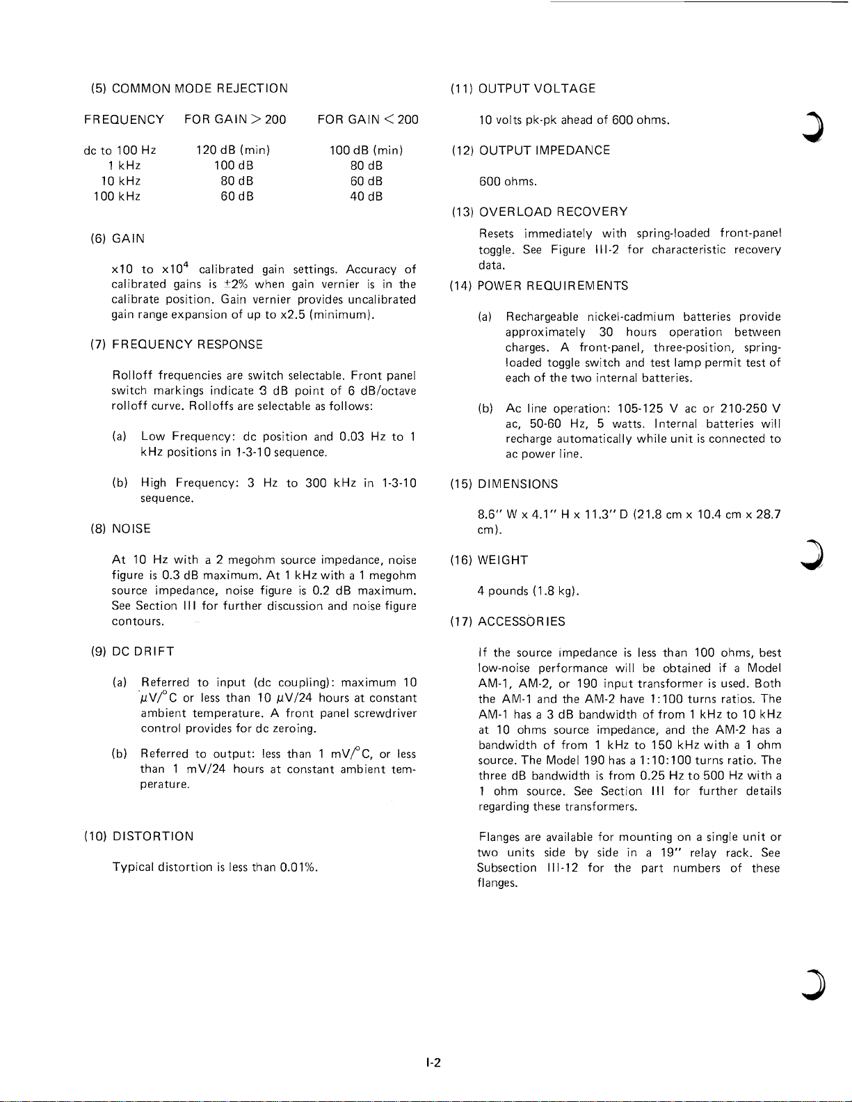
The power cord plug provided is
S.L\"/Hddv
trated in Figure
"N09 3/\|lQ3-1-Qad 3H1 :10 NQU-dnaaa.-|-NI
patible with the available power sockets, the plug
or
power cord should be replaced
ed
type
of
qsuqo
sum,
'1,oe1uoo
1e|1no1a>qoos
.I8MOd auq '6nqd p100
uuee
‘snqeqedde
aqoqag
Lquee
Spuedi->0
S! ‘E->U!I
9'41 ‘(9"19J9ddV
-9J!"b9H
BE
Aue
Aq
qquseop
IF
IT
IS
9A!lO91O.Id
CORD
/Iq
PLACEMENT CORD
SAME POLARITY
OR
paleau eq
punoq
WISE A SAFETY HAZARD FROM ELECTRICAL
SHOCK, WHICH COULD RESULT
DEATH, MIGHT RESULT.
When operated from
line cord disconnected, the Model
considered Class
in which protection against electric shock relies
on supply at safety extra-low voltage (SELV) and in
which voltages higher than those
BIA
em
sum,
'/leqes
Joqonpuoo
01,
1BLI1Sn1BJBddB‘$!
9LI1
OB
/(19198) 8V8 U0!1B<>!I¢I"d
generated. When operated battery powered and
with
the line cord disconnected, the voltage levels
inside the Model
HMVW AVW 'I\'/N||NH3.L H.LHV3
3H.I. =|o NOILOEINNOOSICI so
am
acusmo
1.
so aoqswq HOJ_C)CI
If the provided plug is not com-
iE)NlNHVM
compatible design.
10 ‘mqnuqquoo puno16 Lquee UIB1
1BL|J, “1a1depe,,
NECESSARY
e qnouqq/vq pqos
TH
uq peuesuq
e
spew sq
01
qoqeqado
U101!
WARNING!
TO
E POWER CORD PLUG,
qou
Lquee
spew
e/qqqoeqoqd e
P919Jed0
5'!!!/1999!/V 9!U0J19='-1/3
uoqqoe
qsnuq
OR
PLUG
peqqnbeq auq L|1!M pepq/\o1d
AS
THE ORIGINAL. OTHER-
sq
1e/vqod euq
uoqqoeuuos
uoqqoauuoo
sq
pue
quauqdqnba
its
internal battery with the
118!!!
III
apparatus, that is, apparatus
WSINVHOEIW
113
will
does not take into account the
higher voltages being applied via the signal input
CFIHOHS ll .LVHJ. GNV 3:IVSN 38
LON
or
output
.L| .LVHJ. HHSH
AVW
TO
OJ. CIHEDDVJ. 38 (TIFIOHS NOl.LVO|:I|H3A
HO:|
E)N|J.|VM
BE
D.
'HEId 30!/was <1a|=||-qvno A8 (]EII:III;I3A N338
Before plugging in the power cord, make sure that
AJ.EI=IVS
SVH
the instrument is set for operation from the
(]‘lOHS
voltage
CIEIEDVWVCI
-dv
38
CI'IOQ
cables.
POWER
Sivblvddv (]EI'9VV\IVCI 'S.LVHVd
of
EDNICINIIOHE) EIAliOEI.LOHd EIH.L
'lV|.l.N3J.Od
SJ.VHVddV CIHQVWVG “IHNNOS
VOLTAGE SELECTION
S.LI 'IIJ.N
the ac power supply.
NI 3AIJ.OEI;I=IEINl CIEIHEICINEIH
(JEIJ.VHEIdO 38 J.ON
CAUTION!
THE APPRATUS DESCRIBED
MAY
BE
DAMAGED IF IT
110
FROM
eul
01
9993
10;
uoqqoedsuq
Aq
APPLIED
99 '.I9I.IJBO
ems
Aqqlou
The line voltage is selected by means
peqoedsuq
panel switch.
V AC AND TURNEDON WITH
10;
TO
‘paqou
aq
JGUIBIUOQ Buqddqus eul e/\es
THE POWER INPUT CONNECTOR.
am
q.|1q/v\
sq Aue
pqnous
FOR
IS
wqeqo
qq
smeqedde
SAFETY, UNPLUG THE
'SOH3'5)NV(]
of
with
ue
qo esn
REPLACE THE POWER
uoqsuaqxs ue
e/qqqoeqoqd euq_
MUST HAVE THE
qqeus
Aquo
qo 6uo1d [JUHOJ5
IN
a/qqqoaqoqd
10;
uoqqseuuoo
01
‘Sn1B1Bdd9
UQIIM
OEII
‘BIL IQIJQW
PQUIIGP
U!
of
M.EI=IVS
nofexceed ± 12
'(]3_|_v53¢|0
V
O.L
IN
THIS MANUAL
SET
FOR
e eqqq
'a6ewep
pe/qqeoaq
NO|.L33dSNI '8
'esn
1°! Paulsep U99‘! SP" Snlwdde P9q!1°$9°
'“°!1!P“°° 919$
E
uoqleqado
L
019/\9LI1BLI1$5U!
I\?"“9w
99!!
8!!
If->P°W
IS
queuqnnsuq
uq
e
='-JJHSUB
-U19/I/\
01198"
PUP UQIIPLWQIU!
L=
N
=NEUTRAL
U0!l0nJ1SU!
E =
aqoqag
Figure 1. POWER CORD PLUG WITH POLARITY INDICATIONS
eul, uqelaq 01
919$
LINE
EARTH
9H1/(Q
OR
P9/V\°||°I
9"-10$
9 U! D9!Idd"$ U996!
ACTIVE
CONDUCTOR
OR
IDENTIFIED CONDUCTOR
9!!!!
OR
SAFETY GROUND
peag)
pus
9Q
SUIEIUOO
(ALSO CALLED "LIVE"
LIQIUM 01
N()|_|_Q(]()\;|_|_N|
the type illus-
XNV
an
approv-
'sueau1
‘qoqonp
Aq
esn
qo
TH
ERE·
pqoa
6n|d
INJURY
.I8L|1O Aue
sum,
OR
pun016
113
1°!
SELV are not
uo
could be
I SSBIO
91119!-U
SV
'0
V.
This
possibility
3J.VQ|CIN|
A.L3:lVS
OPERATION
'.I8!.IJEO
220 V AC
pus
Qgvcq
Buqddqus
of
a rear·
Aq/v\aN
.I00pUI
Gui
eqes
9!LI.L
$9!IddB
OR
"HOT")
9LI.L
‘V
N»
M)
‘
of
W
Page 8
—_---up
POWER CORD
POWER
VOLTAGE
VOLTAGE SETTING. Depending on the switch
position,
position, either
the
the switch) will be visible
operation
operation from a line voltage
ac,
ac, the switch should
For
For operation from a line voltage
230 V
230
E. LINE
E.
The Model
The Model 113 line fuse is located inside the in-
strument.
strument. To check or replace the fuse, it is first
necessary
necessary
shield
shield mounted on the inside
The
The fuse should be a slow-blow type rated at
either
either 1/16 A (115 V Operation) or 1/32 A (230 V sion
operation).
operation). The voltage rating should
higher in the case
higher in the Case 01 115 V Operation and 250 V or characteristics
higher in the case
hiélherththe eeee Qt 230V0DeFeti0i1-9h|YeBU$$
MDL
MDL OF equh/eteht
TO
TO
ARD FRQM E|_ECTR|CA|_ SHQCK wi-ii(3i-i (3QUi_|3 and
ARD FROM ELECTRICAL SHOCK WHICH COULD
REsui_T |N INJURY OR DEATH, |)|$(;()Ni\|EcT operating
RESULT
THE PQWER CORD BEFQRE REM()V|NG QR |i\|- one
THE POWER CORD BEFORE REMOVING
$"i'Ai_i_|N(3 A FU$E_ i3E(;Ati$E QF Ti-ii; PQTEN- general use.
STALLING A
T|A|_ HAZARD, Ti-ii; FUSE Si-|()U|_[) BE CHECKED considered
TIAL HAZARD, THE
AND/OR
ANDIOR CHANGED
"|'E(3i-i|\ii(3iAN ()Ni_Y_ plifiers
TECHNICIAN ONLY.
A prooeoure for geinino eooeee to the fuse operating
A procedure for gaining access to the fuse
follows.
follows.
(1) Remove the top oover_ it is eeoureo by e general,
(1)
(2)
(2)
(3) After oheokino eno, it eppropriete, ohenging any
(3)
F.
F.
In
the
In
the past few years, safety
plications
plications has been a matter
to
to
equipment.
equipment. It has long been known that electrical
currents
currents passing through the heart can interfere
CORD WHEN CHANGING THE LINE
either “115”
switch)
from
switch
the
operation
“23O”
ac,
V ac,
"230"
LINE FUSE
FUSE failure,
To
mounted
fuse
should be a
1/16 A
or
equivalent fuse should be used.
AVOID
AVOID THE POSSIBILITY OF A SAFETY HAZ-
IN
CHANGED
Remove the top cover. It is secured by a
single screw
Single screw on the bottom surface
oover “tip” et the reer of the inetrument_ with agination
"lip"
cover
screw removed,
the
the screw removed, the cover simply slides
back
to
back to where
ment_ The
ment.
Remove
Remove the shield attached to the inside
rear panel. This shield is secured by
the rear panel. This shield is secured by a
the
einoie eorew at its oenter_ with the ehieio ed
Single screw at its center. With the shield
removeo, the iuee hoioer, iooeteo oireotiy unnecessary risk
removed, the fuse holder, located directly
above
above the Line Voltage Selector switch,
becomes accessible.
becomes accessible.
After checking and,
fuse, remount
the
the fuse, remount the shield and top cover
before
before plugging in the line cord and operating
the inetrument_ 113
the instrument.
OF THE MODEL
USE
USE OF THE MODEL 113 IN
BIO-MEDICAL
BIO·MEDICAL APPLICATIONS
past
both
the
both the users and suppliers
passing
WHEN CHANGING
SETTING.
"115"
will
a line
should be set
from
should show. use
should show.
113
line
check
remove
to
to
remove the top cover and also the
be
on
Depend'ng
(both
“230”
or
or
"230"
visible
voltage
be
a
line
fuse
replace
or
the
the
(both
to
the
to
the operator. For
of
of
so
set so that "115" shows.
that
voltage
is
located inside
the
cover and also
top
inside
of
of
slow-blow
(115
V operation) or 1/32 A
The voltage
THE
POSSIBILITY o|= A SAFETY HAZ-
INJURY
FUSE.
on
at
where it
shield
the
Line Voltage
the
plugging
rating should
of
115 V operation and
of
230
V operation. Only a
Sheuld be
thee
wA|=tNiN(;i supply
WARNING!
OR
DEATH, DISCONNECT
BECAUSE OF THE
FUSE
SHOULD
BY
A
BY
the
the rear
can
it
can
QUALIFIED SERVICE
A QUALIFIED SERVICE
bottom surface
of
the instrument. With
cover simply slides ie9eTded
the
freed from
be
be
freed from the instru-
attached
if
appropriate, changing
shield
the
in
line
the
cord
113 IN
THE LINE
on
are
are
switch research has shown
the
printed
printed on
operator.
nominally
nominally
“115”
of
of
115 V
115
shows.
nominally
nominally
the
fuse,
rear panel.
the
the rear panel.
type
be
be
USed-
BE
CHECKED
to the
first
it is
rated
(230
125 V
125
V or
250 V or
BUSS
OR
POTEN-
ofthetop-
of
the top-
instru-
the
inside
Selector switch, he evetdeti
and
and
cover
top
operating
1
APPLICATIONS
few years,
has been
users
It
has
safety in bio-medical
a matter
and suppliers
long
been
through
known
the
in
of
of
heart
bio-medical
growing
growing concern
of
of
concern
electronics
electronics
electrical
that
can interfere these
with
normal heart
with normal heart functioning. However, recent
research has shown that danger exists at far lower
on
For a consequence
V
in- high input
the
at
V
or
IN-
of
of
1
ap-
ap-
current
current levels than was previously suspected. As
a consequence
after a careful analysis
after a careful analysis
EG&G
EG&G
feelsthat it cannot recommend the Model 113for
feels that it
use
patients. In
patients.
conditions
conditions
failure, or excessive common-mode input, the
high input impedance
and
and potentially dangerous currents could flow
through the
through the subject.
However,
However, the reader should not get the impression that the Model 113 is in any way a dangerous
instrument
instrument
characteristics that necessitate the adviSOry
against
against the instrument's use in bio-medical
plications with
plications with humans are common
preamplifiers as
preamplifiers as well.
supply voltages, capability for internal battery
power with complete independence
power with
and extremely high input impedance under normal
operating conditions, the Model 113 is probably
one
general use. For all practical purposes,
considered
mum internal supply voltages applied
mum
plifiers are only
can
can only appear at the input under very specific
operating conditions, and then generally for only a
few
few milliseconds. A person inadvertently touching
the
the input under these conditions would, in
general, not even be aware that there was any
voltage there at all and by no stretch
Vettege
agination could the operator
regarded
The preamplifier can be used in biological appli-
cations
cations involving animal subjects. However,
application is one in which skin resistance is
eppiieeiipn
a
greatly reduced
dreetivredueed prbvpeeeed.tne
ed
unnecessary risk to the experimental animal is
be avoided.
(1) Turn
(1)
(2)
(2) set
(3) Do
(3)
It
It may prove helpful
these precautions. By understanding them, the
levels
Princeton
Princeton Applied Research Corporation
cannot recommend the Model 113 for
in applications
in
applications involving human subjects or
certain situations
In
certain situations involving specific
of
of
excessive
or
impedance of the
potentially
subject.
the
that
the
to
to
instrument’s use
the
voltages,
epinpieie independence of
extremely
conditions,
of the
of
the safest preamplifiers available for
to
to
internei
are
only
appear at
only
conditions,
milliseconds.
input
under
not even
there at
could
as
being
ee hethg
preamplifier
involving animal subjects.
ie pne in whieh ekin reeieienee is
to
to
observe the following recommendations
observe the
the
Turn the amplifier power on BEFORE making
connections
any connections
Set the Input Coupling switches
the
thput
113
the experimental animal.
the
the
the GND settings until after the connections
are
are
Do
the
the instrument is connected
mental
mental animal.
may
GND
to
GND before making any connections
to
experimental animal.
GND
completed.
completed.
not
turn
not turn the power switch on
instrument is connected
animal.
prove
precautions.
functioning.
dangerexists
that
was previously
than
of this
of
increased
this
increased awareness, and
of
of
Applied
involving human
grounding,
grounding, internal component
However,
at
recent
far
lower
suspected. As
awareness,
the Model 113 design,
the Model 113 deSign,
Research
Corporation
and
subjects
involving
specific
internal component
common-mode input,
of
Model
the Model
dangerous currents
reader
Model
use in ordinary applications.
use in ordinary applications. Those
should not
113
is
in
any wayadangerous
that necessitate
are
humans
well. In
capability
high input impedance under
safest
For
all practical
be
completely harmless.
be
completely harmless. The maxi-
Supply
12 V. Even
i
±
12
the
A person
these
be aware
ett ehd hY he etfeteh Qt the im-
the
operator
in
ih
can
or
bypassed, the operator is advis-
following
to
the
amplifier
Ceuhtthg ewttehee 01 the Medet
before
settings
power
the
helpful to consider the reason for
By understanding
common
fact,
In
with
fact, with
for
Model
the
preamplifiers
vpitepee
V.
Even
input
and
then
inadvertently
conditions
that there
of
of
any danger.
ehY dehgeh
be used in
recommendations if
experimental animal
power
to
to
on
experimental animal.
the
the experimental animal.
making
Do
Do
after
until
switch
to
consider the reason for
113
could fail
113
could fail
flow
impres-
get
could
the
Those
advisory
the
in
bio-medical
most
to
to
its
low
its
low internal
other
most other
internal
internal battery
of
the ac line,
the ep
113
is
line.
normal
probably
available
purposes,
eppiied tp the em-
these low voltages
these
under
can be
it
it
can be
The
maxi-
to
the am-
voltages
low
very specific
generallyforonlya
touching
would,
was
any
of
the im-
instrument
the
the instrument be
biological appli-
However,
pperetprie
if
if
advis-
isto
BEFORE
any
connections to
not
not transfer from
the
on
to the
to
making
of
the Model
transfer
from
connections
while
off
or
or
off
while
experi-
the experi-
them,
or
the
ap-
ap-
for
in
be
the
the
to
to
the
3
if
Page 9
1
i
operator may be better able
electrical
only
but where
(1)
monitoring
where the input
other
of experimental animals, not
amplifier
preamplifiers are used as well.
Turn-On Transients
When the
cuits
amplifier
do not instantly assume
operating state. Instead, a
to
safely carry out
is the Model
is first turned on, all cir-
their
quiescent
finite
time
quired for the common-mode loop amplifier
to
ing point. During
'|euu0s1ed
A12-112s
from a few
s11
set the input stages
001/ues pe111|enb
|11un
milliseconds
eq10u
pasn
to
their proper operat-
this
interval (which varies
pe1111a/\
Aq
to
p|n0L1s
a second
sn1e1edde
ueeq seq
depending on the source impedance), the
source-gate
or
uvdsuen we/\es O1
the
the
transistor
pedance, but instead appears as a low im-
pedance from the input
e6e101s
‘s1ueu1e1nseeu1
pe6u0|01d
the
output
(2)
Power Transformer
junction
other
is forward-biased.
‘su0111pu00
01 pe10e[qns
of
the common-mode amplifier.
pepue1u1
of
one input transistor
D9109[q"$
does not
exhibit
a|qe10/\e1un
of
the instrument
0111
111101100
‘eewep e|q1s1/\
'sesse11s
In
ueaq $91-| (v)
this
a high im-
1epun 1210/\es 012
uaeq
se|_| (9) 1eu11e
01
s|1e:|
s/v\0q3
The power transformer in the Model
very high quality and is unlikely to fail during
life
of
-u1exe101‘11pe11ed1111eq
e/\11e1ed0u1
-u11 uaaq
the
'u0!1B19d0 pepua1u1un
possibility
must
and
if
seu
complete
pep;/101d
u0110e101d
the instrument. Nevertheless, the
of
spew aq ||eus sn1e1edde
be considered. Should a short develop,
the
instrument were being used
pun016
or
mon in many
-“IWHONHV GNV
dangerous situation would exist.
(3)
Internal Component Failure
01/(|e>11|s1u0110e101d eul
Aue
such a failure, however remote,
1111120 01
improper ground returns (com-
eul
1€u1
buildings
The input transistors
junction-type
e1n1e1ed111e11ue1qu1e 011112111
eq
though they
0111
/§|u0
5U!1Ul'1OLU
eq
Aue
-1eq
“GUM 9119'“
‘(A1010121
resistance when properly biased,
>10e1)
tance can drop
ueo
ing current or bias is
a/ueu
ing range
ueu/v\ sse|
biased diode
the source or the drain. There are several
's1ue111e11nbe1
1|
10u
9 MUD 4° u°!1dw"Su°°
‘£3,912
field-effect
exhibit
111011
0111
>10e1
e
to
911
seop
sufficiently
ue/10
pue
junction
u!
|ep0|/\| 0111 ‘pe1e1ad0
‘eu||
possible internal component failures which,
though unlikely, could bring about
tion. Should
fier
would be connected through a low im-
pedance
s1su0g1e01|dde1eu10||eu1esn
L111/v\ esn
u011e10d109
L|5HOL|1
supply.
101
ue/\e
911
‘1eu1pez1seL1d1ua
it
occur, the input
directly
-u011e/\1ese1
|ep0|/11
qomeseg
to
0111
peuddv
:sn1e1edde
1su1e6e
pemoes
0111
u0110euu00
s1 11 10/\eueu/1/1
A|e>11|
and installations), a
33333313
$133530 -H
of
the Model
01O<,9L
an
paseuomd
10
a few
out
to
-
the
1n0u11/v\
pue1u11100e1
4°
95°91
transistors.
6u1eq
extremely high input
uoueq e
ohms
u011e|11ue/1
of
give a simple forward
0e
e111
from the gate
eq
u0 pe1e1ad0
if
their
the normal operat-
u1011
J9M°d 9 WM
N0|-|-V'||1-N3/\
of
instrument's
pepua1u1u00e1
s11‘s10e[qns
u01e0u11d 91993
eq p|n0us
0111
1u1e11su00 JO Q EH Iapow
ueo
their
pe1e1ed0
this
the ampli-
10u
11
'a0ueped -110
-11111ndugau11a/v\0|Aqe1eu1pue‘s11n01101ndu1
ehll
1001010
'su11
u0110npu00
/\ 1 s1 911
squad
-UOLULUOO
01 10111101112010 eL|1101ndu1
/v\0|
|ep0|/\|
‘su011e01110eds
0111
1ndu|
“uo u1n1,,
0141101111111
epow-u0111u10Q
s10/\e|
eu1
011112
10116114
1ndu1
pelels
ug
0/\1sse0x3
epow
(4)
Excessive Common-Mode Input
113,
As stated in the specifications, the common-
mode input
Higher levels
at the input
input circuits, and thereby lower the
pedance.
is
re-
Again, it should be emphasized that, even though
EG&G Princeton Applied Research Corporation
does
not recommend the Model
human subjects,
or
more
uong 10/v\0d s,1ueu1n11su1
state,
to
(3)
(1)
113
is
of
‘e|d -|v 's101s1sue11
recommended
-LU! /v\0| e u6n01u1
1ndu1
10
-g|dwe
-!r>u<>vs!u11r\<>qv
‘uogu/v\ se1n|1e1
p1e/v\101a|du11s
-1e1ed0
-1e1ed0
-s1se1 110111
1ndug 115111
012 911
eu1
G. VENTILATION
With a power consumption
operated from the ac line, and even less when battery operated, the Model 113 does not have any
special
operated on a bench or
kits can
constraint being that the ambient temperature
in the range of 15°C to
010111
010126
|e1u10u 011110
ventilation
11eu111
‘pese1q
be
purchased from the factory), the only
A|au1e11xe
|ep0W
pue
‘pe11ed
with
in-
0111 Aq
113
W1“!
s1!>1
resis-
operat-
|e10eds
A101
to
either
'9
condi-
1
power
uewnu
seop
‘ugev
sv
(11)
are
Al-
H.
DEFECTS AND ABNORMAL
STRESSES
‘(su011e||e1su1
12
-11100)
Whenever it is likely that the protection provided
-ug L|1!M
by the connection
‘d0|c-map
paired, the apparatus shall be made inoperative
‘e10111a1
and secured against any unintended operation.
0111 ‘sse|eu11e/\eN
The protection is likely
fiuunp
ple, the apparatus:
'
(1)
(2)
'1s1xe
su1n1a1
Bugeq
pesn
110us e p|n0L13
10/\a/v\0u
112101/(|e>11|un
Shows visible damage,
Fails
to
ualmdwe apouwowwoo
O - '
(3)
Has been subjected
11ueu1n11sug
-LUI
101s1sue11 1ndug auo
0111
-121:-ado 1ad01d 110111
1e111|du1e d00|
under unfavorable conditions,
(4)
‘a1e1s
/v\0|
116111
se sfmleeiide
e
e 11q1uxe
Has been subjected
u|
S!Lll
stresses.
‘(eouepadwg e01n0s
Such apparatus should not be used until
e10u1
has been verified by qualified service personnel.
sa->112/1
-e1
1ue0se1nb
"||a/v\
‘QLL
10u
1n0 A1120 A|a1es 01 e|qe
puooas
10
uogum)
s1 011111
‘u0
112
se pesn
|ap0|/1|
‘s|eu11ue
e11u11
11:->u1eu1nsse A|1ue1su1
peu1n1
01.11
|e1ue11111edxe10
limit
of
the Model 113 is 1 V rms.
"turn
on"
low
conduction
of
the preamplifier to protect the
113
for use
its
use in all other
01 A|10e11p
au1
without
Buuq
reservation.
pe10auu00
eu1 ‘1n000
PIHOO ‘K|<->>1!|l1r\
eq
11 p|n0u3
1ueu0dw00 |eu1e1u1
-u1e1p
eu1u101;
e e/116
swuo
A|1ad01d
100110-p|e11
10
9L|1
a1n|1e5
p|n0/v\
pue
u0110un[ ep01p
A|1ue10111ns a6ue1
01
1n0 s1
requirements. It can be
M012
ue
s101s1sue11
s6ugp|1nq
10
eu1
of
segq
d01p
01
in
a rack (rack
ueu/v\ a0ue1s1sa1
11q1uxa
ed/(1-u0110un[
45
°C.
1uau0dw0Q
u011en11s
pun016 1ed01du11
e1a/v\1ua11|n11su1
to
earth ground has been im-
'pa1ep1su00
‘e1n|1e1e
'1ue1un11su1
eu1u|JewJ0JSueJU9M0d
perform the intended measurements,
e
01n
1
-pesegq-p1e/v\101
01
e
|e/\1a1u1
01sa5e1s
apomu-u0111u100
e ‘pee1su|
1s111
012 s1e111|du1ee1d
s1 1e111|du1e 1ndu1
u0ns
0111
to
be impaired if, for exam-
pue
s1
'
Mllenb 116111
1eu1101sue1_L
em ;0 mdmo em
d
to
ug 0
111101
pee1sL1|1|
10u
sa0p'101s1sue11
to
s1 101110
10 u0110un[
u0
0111
spu00es1||1u1
6u11nq
S!l41
1ndu1 0'41
01.11101
'e1e1s 6u11e1ed0
1e111|dLue
sq
S1UG!SUBJ]_ UQ-Ulni (1)
5ug1011u0u1 |e01110a|a
1a11aq
"A|ddns
applications
asueped
p|n0/v\
u5r\<>u1
e|q1ss0d
e01n0s
only 5 watts when
pasegq
101ue11n0
ueo
e0ue1
A0111 u6n0u1
1ndu1
|eu1a1u|
sn01e6uep
Auew
u1
10 e1e|d11100
011111
eq 1snu1
A11|1q1ss0d
10
10 0111 0111
1e/v\0d
prolonged storage
eoue
1nqJ‘c-Jouegad
severe transport
au1 10
0126-e01n0s
ugpuedap
M8}
e 111011
'1u10d 6u1
les
pe11nb
10u op
eu1
1eu10
eu1
01011/v\
aq A2111
paths
input
1011
-u011
0111
6ug
6u1
mounting
aui
(9)
u0u1
pue
A10/1
Gui
(3)
d
0
0111
its
safety
01
s11n0
ueu/1/1
a1eu/v\
A|u0
101e1ed0
im-
with
be
1nq
is
’
1
W
Page 10

L'\
SECTION
CHARACTERISTICS
1.1
INTRODUCTION
The Model 113 Low-Noise Preamplifier provides high gain,
low
noise
amplification
kHz. Adjustable high and
bandwidth
to
be
coupling switches,
operation. Calibrated gain
X104
in a 1·2-5 sequence, and
provides
The
unit
x1
to
x2.5 range expansion.
may
be
powered either
own batteries. The nickel-cadmium batteries recharge
automatically
during line operation.
Other features include
special
circuitry
currents, front-panel
tion
screwdriver controls,
The Model 113
other Princeton
is
Applied
ments.
1.2 SPECIFICATIONS
(1) INPUTS
=(>|
009$
unwul ooz
01
Two
channels,
provide
tial operation. I
for
1(00l
of
wideband signals
low
frequency
reduced.
allow
Two
either
differential
is
switch selectable
an
from
an
overload fast-recovery switch,
that
reduces the effects
dc
zeroing and common mode rejec-
and
battery
well suited
for
Research signal processing instru-
40 ww) apvw
each
with
a three position switch
ac
or
dc coupled, single-ended
nput
SW95)
connectors
A
.SwJ
O1 OLJO
from
dc
to
300
rolloffs
inputs,
allow the
with
individual
or
single-ended
from
x10
to
uncalibrated gain vernier
the
ac
line
or
from
its
of
ground-loop
test provisions.
use
as
QPOW
are
BNC
L Iepow
a preamplifier
'/\LU
l9!1U919H!Cl
.Aw
or
I9!1U919H!C|
type
uowwoc)
09$
differen.
for
(O)
to
(Q)
(E)
I
(2)
INPUT
(a)
(b) Dc coupled: 1 gigohm, shunted
(3)
MAXIMUM
(a)
l
(4)
-ua1aH!p
01
-H.l1SU[5U!SS800.Id
J0;
IMPEDANCE
Ac
coupled: through
with
100 megohms and 15 pF in parallel.
INPUT
WITHOUT
Dc coupled: Common-Mode,
(b)
tial, ±7.5
Ac
200
V.
coupled: coupling capacitors can
V. Transients
capacitors cannot exceed dc coupled operation
limits.
MAXIMUM
LINEAR
(a)
Common
Differential
(b)
mY.
L|O1!/V\S
(c)
Differential
±50
J9[}!|dLU€G.lC|
INPUT
OPERATION
mode: 1 V rms.
QN9
"ad/\1
pepua-a|6ugs
JO
UO[l[SOd
mY.
smlaauuoo
am
mode (gains
aanp,
mode (gains
|eu6!s
asn
se
2
0.1
which
SIGNAL
(see
Subsection 3.10)
‘pa|dn0o
qlg/v\
e
SNO|_W3H|33dS
qzueasag
palms
Jo;
J.1F,
shunted
by
15
DAMAGE
±10
V;
pass
through coupling
CONSISTENT
'uo!1e1ed0
1ndu|
of
10
to
10;
oe
10
op
’s|auueqo
qoee
of
200
through 10
paqddv
sg gll
||a/v\
to
ground
pF.
Differen-
withstand
WITH
|eg1
100):
±500
8p!/\O.lC|
0/v\_|_
S_LdNl
uolaauud
|apo|/\|
k):
(L)
Z1
'S1Ll9LLl
J9L|1O
aq_|_
J
*
w
~
LNELLSISNOD
H_LlN\
UO!19.l9dO
/
6ug|dno:>
pue1sq1g/v\
-umeggq
pun01
(UL-8
pa|dnoo
q
5no1
ueo
5/\
El'E)\7’V\|V(]
Wauejed
palunqs
01
ugugggqns
"lVND|S
paaoxa
op
ssed
q
agq/v\
[41
smlpedeo
'apoW-uowwog
Q[_:|:
.LOH_LlN\_LdN|
pa1unqSluJqO5!5L
dd gt
U!
1'9
‘511
NO|_LVH3dO
995)
.LdNI
louueo
s1uagsue1_|_
6u!|dn0a
:pa|dn0:>
'/\
:pa|dno:>
zpaldnoa
Swqoaw
pug
q6noJq1 :pa|dnoo
EIf)NV(]3dV\l|
HVBNH
INHINIXVI/\l
'$1!W!l
s101goede:>
QQZ
'/\
av
9'L¥'|9!1
sq
INHINIXVW
(17)
(q)
(9)
(8)
90
Lm,“
Om
(e)
av
_LdNl
(Z)
SQILSIHHLQVHVHO
NOLLOHS
I
\-1
'suogsg/\oJd
apow
-i)9[9J
dOO|-pUI'\O.l5
‘qolg/v\s
a61eq:>e1
s13
.l8[UJ9A
01 QLX
papue-e|5ugs
|Bl"|p[/\!pU[
aql
QQ8
‘uge
Ma/\o0aJ-1se;
saualleq
10
LUOJ}
uge
11.101;
/v\0||e
01 op u.|o1;s|eu6gs
qgq
1sa1
uowwoo
s1oaHa
;0
oe
au!|
pe1e1qg|eoun
e|qe1oa|as
|B[1U9J9H.[p
JO
'S1dU[
s;;0||o1
sap!/\01d
Malleq
Bugmaz
pue
seonpeu
aql
peope/\0
'UO|1€J8dO
.
wngwpeo-|a>|9gu
.l8q1[9
LUOJ}
eql
'u0gsuedxa
pue
ue
qslg/v\s
Jaqlga
ON\_]_
Aouanbaq
pueqep!/v\
1ag,u|dweeJd
pue
ue
’a0uenbes
sg uge
'pa0npc->1
/v\o|
40
as!o|\|-/v\o"|
's|011u00
0p
apn|oug
au||
pe1e/vxod
95UBJ
/v\0||e
pue
J9A[.lpN\9JI)S
|aued-1u01;
Angnrugra
12141
Buunp
.
.
aq_|_
aq
ggx
p91EJC|[|BQ
'saqo1g/v\s
eq
e|qe1sn[pv
qgq
uogleogmdwe
NO|J.I)ClOHJ.N|
'S1U€-LLIHO
|eg0eds
samlea;
A||eo|1eLu01ne
.
'sag1e11eq
lgun
Aew
S9p[AO.|d
Lx
01
ug
e
9-Z-L
'uog1e1ed0
5ug|dnoo
L|1p[/V\pUBq
O1
asgou
|epo|/\|
gll
uo!1
Jaqlg
u/v\0
eq_|_
tglx
'z|_|>|
/v\0|
eq_|_
L‘
L
Page 11
(5) COMMON
(5) COMMON MODE REJECTION
MODE
REJECTION
(11)
(11)
OUTPUT
OUTPUT
VOLTAGE
VOLTAGE
FREQUENCY
FREQUENCY
dc
dc
100
100
(6) GA|N
(6)
(7)
(7)
(B)
(8)
Hz
100
to
to
100 Hz
1 kHz
1 kHz
kHz 80 dB
10
kHz
10
kHz 60
kHz
GAIN
x10
to
x10
to
calibrated
calibrated gains
calibrate position.
calibrate position. Gain vernier provides uncalibrated
gain range expansion
gain F8099 eXl3>an$i0n
FREQUENCY
FREQUENCY RESPONSE
Rolloff frequencies
Rolloff
switch markings
switch markings indicate
rolloff curve.
roll
off
(a)
Low
(8) I-OW FFBQUBHCVI
kHz
kHz
(b) High Frequency:
(b) High Frequency: 3 Hz
sequence.
sequence.
NOISE
NOISE
FOR
GAIN
>
FOR
GAIN>
120
dB
120 dB (min)
100
100
BOdB
60
x104
calibrated gain settings. Accuracy of
X104
calibrated gain settings. Accuracy
gains
is i2% when gain
is
Gain
RESPONSE
frequencies
indicate 3
Rolloffs
curve.
Rolloffs
Frequency:
positions
positions in 1-3-10 sequence.
in
200 FOR GAIN < 200
200
(min)
dB
dB
dB 40 dB
dB
±2% when gain vernier
vernier
of
up
to
x2.5
01 LID ‘£0
are switch
are
are selectable as
are
1-3-10 sequence.
X2-5(fT\ilmUm)-
switch selectable.
dB point of 6 dB/octave
~
dB
selectable
dc
position
d¢ P050100
3 Hz to
FOR
GAIN
100 dB
100 dB (min)
80
BO
60 dB
60 dB
40 dB
vernier
provides
selectable.
point
300
to
300
uncalibrated
(minimum).
Front
of
6 dB/octave
follows:
as
follows:
and
0.03 Hz
and 0-03 HZ ‘E0 I recharge automatically
kHz
kHz in 1-3-10
volts
< 200
(min)
dB
dB
of
is in the (14)
is
in the
Front
panel each of the -[W0 in-[ema|
panel
to
in
1-3-10
10
10 volts pk-pk
(12)
OUTPUT
OUTPUT
(12)
600
600 ohms.
(13)
OVERLOAD
(13)
OVERLOAD
Resets
Resets
toggle.
toggle.
data.
data-
P()\/\/ER REQU|RE|\/|E|\|TS
(14) POWER
(a) Rechargeable
(a)
(b) AC |ine
(b)
(15)
DIMENSIONS
(15) DIMENSIONS
8.6" W
B.6"
cm).
cm).
pk-pk ahead of 600 ohms.
IMPEDANCE
IMPEDANCE
ohms.
immediately
immediately
Figure
See
See
Figure
REQUIREMENTS
Rechargeable nickel-cadmium batteries provide
approximately
approximately 30 hours operation between
charges.
charges. A front-panel, three-position, spring-
loaded
toggle
loaded toggle switch
each
of
the
Ac
ac, 50-60
ac,
recharge automatically
ac power line_
ac
W x
Operation; 195-125 \/ ac
line operation: 105-125 V
50-60 Hz, 5 watts. I nternal batteries
power line.
x 4.1" H x11.3"
4.1"
ahead
of
600 ohms.
RECOVERY
RECOVERY
with spring-loaded
with
spring-loaded front-panel
Ill-2 for characteristic recovery
111-2
for
characteristic recovery
nickel-cadmium batteries provide
hours
30
front-panel,
A
switch and test lamp
and
two
internal batteries.
Hz, 5
H x
watts. Internal
D (21.8 cm
11.3"
D (21.B cm x 10.4 cm x 2B.7
operation bet\/veen
three-position, spring-
test lamp
bat-(erie5_
permit
permit
or 210-259 \/
ac
or
batteries
while unit
while
is connected
unit
is
x
10.4
connected
front-panel
test
test
210-250 V
will
will
to
cm x 28.7
of
of
to
At
At
10 Hz
figure
figure
source impedance,
source impedance, noise figure
See Section
See
contours.
contours.
(9) DC DRIFT
(9) DC
(a) Referred
(a)
(b) Referred
(bl Referred
DISTORTION
(10)
DISTORTION
(10)
Typicaldistortion
Typical
with
Hz
10
is
0.3
is
0_3
Section
DRIFT
Referred
"IlV/C
‘I-IV/QC Or
ambient
ambient temperature. A
control
control provides
than 1
than 1 mv/24
perature.
peratum
distortion
a 2 megohm source impedance, noise
with
a 2 megohm source impedance, noise
maximum. At 1 kHz
dB
dB maximum_
noise figure
Ill for
further
III
for
further
to input (dc coupling):
to
input
or
less
than
I688 than
temperature. A
provides
to
output:
to Output: less than 1 mv/CC’
mV/24
less
is
is
less
At
discussion
discussion and noise figure
(dc coupling):
/1V/24
10
IlV/24
10
for
dc
zeroing.
for dc Zeroing.
less
hours at constant ambient tem-
hours at Constant ambmnt
than 0.01%.
than 0.01%.
with
1 kHz
with
is
0.2 dB
is
0.2 dB maximum_
hours at constant
hours at constant
front
panel screwdriver AM-1 has a 3 dB
front
panel screwdriver
than 1
a 1
a 1 megohm
maximum.
noise figure
and
maximum
maximum
mV/C,
megohm
10
or
less
or less
tern‘ three dB
10
(16) WEIGHT
(16)
WEIGHT
4 pounds
4 pounds (1.B kg).
(17) ACCESSORIES
(17) ACCESSORIES
If
the
If
the source impedance
low-noise
low-noise performance
AM-1,
AM-1, AM-2,
AM-1
the
the AM-1 and the AM-2
AM-1
has
at 10 ohms
at 10 ohms source impedance,
bandwidth of
bandwidth
source. The Model 190
source.
three dB bandwidth
1 ohm source. See Section
1 ohm source.
regarding
regarding these transformers.
Flanges
Flanges
two units side by
two
units side by side in a
Subsection III-12 for
Subsection
flanges.
flanges.
kg).
(1.8
source
impedance
performance will be
AM-2,
or 190 input transformer
or
190
and the
a 3 dB bandwidth
of
The
AM-2 have
bandwidth Qf fr()m 1 kHz
source
from
from
Model
190 has a
bandwidth is
See
these transformers.
are available
are
available
111-12
for
is less than 100 ohms, best
is
less
than 100 ohms, best
will
input
have
impedance,
1 kHz to
1 kHz
has
from
is
from
Section
for mounting on a single
for
mounting
side in a
the part numbers
the part numbers
obtained
be
obtained
transformer
1:100
1: 100 turns ratios. The
of
from
and
and the
150
to
150
1:10:100 turns
a 1: 1 0: 1
Hz to
0.25
0.25 Hz
for further details
lll
III
for
19" relay rack.
19"
if a
if
is
is
turns
1 kHz
AM-2 has
the AM-2
kHz with
kHz
with
00
turns ratio. The
500
to
500
further
on a single
relay rack.
Model
a Model
used. Both
used. Both
ratios. The
to 10 kHz
to
10 kHz
has
ohm
a 1
a 1 ohm
ratio. The
Hz with a
Hz
with
details
unit or
unit
or
See
See
of
these
of
these
a
a
a
I-2
1-2
J
Page 12
L'll
2.1
INTRODUCTION
The
following
performance
procedure
ment
for shipping damage (any
carrier and
but
before using
encountered
factory
or
procedure
checking
of
is
the
should be performed
to
Princeton Applied Research
it
experimentally. Should
in carrying
one
of
its representatives.
out
2.2 EQUIPMENT NEEDED
(1) General
(2) Signal
sL1! 1eq1
sinewave
-19d
luawmlsug
2.3 PROCEDURE
'uog1gs0d
(1) Make sure
indicating
u101;
A|qe1ap!su0:>
Vac).
8L{1
'.l9A8N\O|-| '/\LLl
p|n0qs
(2) Plug
into
'>|d->|d
101Lu0|/\|
(3) Press
(4) Push
sawp,
aql
then
JO1!u0W_>|d_>|d
light for
(5) Make
eq
/\ L
(a) Gain:
sumas 1ndu|
apn1!|du1e
asn)
3l.|l
'>|d->|d
pue
'>|oe[
purpose
generator
ems A|qeu0sea1
at
(1no) :|:]Q
1nd1n0
the
line
the
power receptacle.
/\ L aq p|n0qs
'>|d->|d /\ L ‘z|_|>| L 01 JO1BJ8U95
the
the
ua1 aq p|n0qs
push
both
the
p|noqs
until
uaa/v\1aq
.|01e1aua6
'>|oe[
A
3N9
1nd1n0 aql
L
'ZH>|
'z|-L L
laboratory oscilloscope.
capable
1 Hz,
aql 4|
aq ueo auo ’pa1eogpug
100
Hz, and 1 kHz.
's>|oaqo Leglgug
aql 01 L|C)1!N\S J9MOC|
the
rear-panel slide switch
the
line voltage
Me/\ uea
Q9 A||e0gdA1
9l.|1 fu011nq
cord
apn1!|dwe Leugs
Me/\00a1
into
the
La/\a| 1nd1no sq), f1nd1no
power switch so
spring-loaded
it
to
,ZH
La/\a| 1n
the
battery
right.
positions.
following initial
La/\a| 1nd1n0
x10;
the
switch
aqa,
Cal.: fully counterclockwise
"clicks").
A:>ua1s|suoo
|eu5gs aql
;)|\|g lndug
IZH
L
L
01 1o1e1aua6
01 ado0s0||!:)s0
Il0J1U09,l,l0||OH
1|OJ1UO1)HO||OH
INITIAL
provided
Model 113.
after
noted
these checks,
of
to
‘|a/\a| /v\o| e 01 aseamap
that
d
1n0
The
Jolejaua
control
51nd1no
('s6ugpea1
a>Leu1
V
/\:>uanba1:L
to
facilitate initial
In
general,
inspecting
to
be reported
the
Corporation),
any
difficulty be
contact
'A|Jad01d 5U!18J9dO
providing a 1 V pk-pk
aqn, sa1a|dwoo
be used
eql
is
'1!un
(115
in
a1n|0sqe
se pauuo;
umlag (ZL)
the
01 1Lun
V ac
"L/\() aql sseud (LL)
rear
of
the
instrument
aql
Leugs aql 1a3 (QL)
it remains depressed.
test
toggle
to
lndu!
-lam‘
f d
1n0 9141
1n
aql
green indicator should
‘Bums
settings:
'>|d->|d
101guo|/\|
aql
pue
loauuoo
19$
laauuog
q5!|_|
/v\0"|
u|e1q0
01 ad0os0||g:>s0
01
8L|1
|eu6gs aql
aql
Aou:-)nba1;L
1nd1n0
01 ‘s6u|11as
1!
SECTION
the
instru-
to
the
the
s!|.|_|_
position
or
220
and
the
left,
(6)
(3)
(turn
(L)
(9)
(p)
(0)
II
CHECKS
(b) Coupling: A
the
Frequency
Frequency
the
signal
it
(c) Low
(d) High
Connect
(6)
Set
(7)
connect
oscilloscope
settings,
and
as;/v\>|00|01e1un0:> A||n; :'|eQ !QLx zugeg (2)
uml)
(8) Monitor
pk-pk.
(9)
Set
p|n0qs JO1BO[pU! uaa16 aqi '1q5[J aql 01 1; qsnd uaql
the
9L|1 01 a|6601
‘1;a|
input
'p8SS9Jd8p
(10)
Set
the
pue 1uaLum1suL
(11) Press
decrease
absolute signal
JO
QZZ
oe /\ 9L L) pasn aq 01 a5e1|0/\
unit
uoglgso sq), ug sq
(12) Return
to
output
the
:s6ug11as
the
signal
output;
level.
sugeweu 1g1eq1 os qf)1!N\S J8IV\Od aql ssc-ud (3)
the
signal
output;
aq),
the
to
to
unit.
the
This completes
formed
>|d->|d
operating properly.
as
/\ L e
indicated,
Bugpg/\01d
edoasomaw
aql 1oe1u0:) ‘s>|oaqo asaql 1n0 Bug/X11129 ug pa1a1uno:>ua
aq /\1|n:>g;Lgp Aue p|OL|S
'(U0!1B.lOd.lOQ
01 panodaj aq 01 palou Aue) aewep Bugddgqs 10; luau;
aq1
amp,
-nnsug
’|e1aua6
aqn,
l9!1!U! 9191!|!99}
qomasag pauddv uolaoupd 01 pue J9!.lJBI)
ugmadsug Jaye pauuopad
u| 'gLL |ap0|/\|
input
AC, B
input
GND.
Rolloff
Rolloff
oscilloscope
generator
to
the A input
to
make
obtain
consistency
the
control:
control:
to
the
to
1 Hz, 1 V pk-pk, and
output
1 Hz.
1 kHz.
BNC jack_
BNC jack. (Use
signal
generator
between
input
amplitude
readings.)
f(,,s>|og|o,,
output;
|OJ1UOO Leglgug 6uL/v\0||0,1 aL|1 e>|e|/\L
generator
the
output
1sa1 Malleq
generator
the
output
L0 1291
OVL
recovery
a low level, typically
amplitude
LL01!/v\s
ap!|s Laue -ma; 8L|1 ems
power
switch
the
initial checks. If
pue ‘z|_|
L
'z|-|>|
one
L0
CHCHQN
LL01!/v\s aql
the
output
'suog1gs0d
to
100
level should be
pepe0|-Bupds
to
1 kHz, 1 V pk-pk.
level should be 7 V pk-pk.
'G|OQld9I)9J
01u! p100 aug| sq], 6n|d (3)
sq),
button;
can vary considerably
au|| sq), 6u|1L2(:>O|iJ:1\|
to
the
ElH(]3OOHd 8'2
QQL ’z|_|
can be reasonably sure
a|qedeo JOlB.l9U95 |eu6!3
Molejoqm
|!1un
level should be 7 V
10;1q5;|
qloq
Hz, 1 V pk-pk.
ten
9141 qsnd
J9N\Od
aql o1uL
the
output
50
mV. However,
.
OFF
.
a>|e|/\|
(out) position.
the
instrument
L12 a/\e/vxaugs
asodmd ‘mama
-|-N3Wd|nO3
times
. .
wmleluasajdal
'/\||Q1U£-)LU!.l9dX9
aql Lo 5U!>|38L|3
01 P9P!'\0Jd 5! 9mP99°1d 5“!/\/\°||°} 9LLL
15 Bugsn a1o;aq 1nq
aq p|noqs
ampaoojd
a0ueuu0,uad
the
settings
(g)
Monitor
the
(17)
Monitor
should
the
from
(L)
per-
that
it
(Z)
(L)
Z2
is
'c1|\|91ndu!
s‘:)v1ndu!v =5u!|dn<>:> (q)
S)lO3H3
NOLLOHS
ll
'lVl.l.lNI
11-1
NOLLOHCJOHLNI
L'Z
Page 13

7-"
S!
Avuanbwq
95!°U
optimum
pasn
uq
the
bandwidth,
which
Q3/:||\|
the
self-contained
a5e1|o/\
to
the
a resistance
sqqq_|_
ueo
1ua|e/\qnba
operating
Aq
uaq/q/q
the
:e|nu.u0qaq1
Jaqlo
“em
‘DP
aw’
3.1 INTRODUCTION
paqqdnqnw
Aq
"z/M
Ll1P!/“PUQQ
4°
9H1
To
obtain
uqleqado
paqdnoo
aql
Op
must
be exercised in selecting
in
selecting
6uququ.ua1ap
tions,
all
of
Fundamentally,
either
and
sun
the
s1|0/\
from
=
signal
connector(s);
jack
through
pauqelqo
asqou
aq
su.u
1ndu|
NOTE: Before
rear-panel switch
voltage
installed
to
SUn0.|.N00
operation).
the line fuse and possibly
qO|
;OP§
'
and
circuit
’
F
3.2 NOISE
s~
L
7
Best amplifier
=°'p
under
those
signal-to-noise ratio. In
$0,?
generated
factor
in
respect, amplifier noise
,o|/
amount
thermal
90!
"Noise
901
(1) Noise Figure =
10»
‘°‘
oqol
s
20
avov
Figure":
I
0910
where
K =
em
T
=
M =
R =
of
9“13G°W
be used,
aunsu
(1/16
A for
Operating
{OI
’O|
components.
~~
AND
performance
conditions
+
by
the
—+~
determining
‘F
“s
noise
the
*~
noise; expressed in decibels, this
total
rms noise voltage
gain x
the
Source
= E,
rms
Boltzmann's
avo
absolute
equivalent
source
temperature
M.
P9
resistance
the
coupling
asqou
aqnqq
pa11o|d
'aoue1sqsa1
The
total
‘amqq
qoqq/v\
input
figure,
ground,
be
pue
aamos
output
noise
expressed
and regard this
1as
qo
zero).
'/kqqeluauqqqadxa
pue
noise may be
oqlsqqalaeqeqo
asqou
by
dividing
in
L;
Zq+
“ii
Z24
OPERATING
L|lp!MpUBq
sq
ua/\q5
umas
muanbau
qqvqqw
1U9l9'\!"b9
'q1pq/v\pueq
performance
9H1
the
qlpq/vqpueq
and
are discussed
instrument
5O||1UB
asqou
be ampl ified
amplified signal
:(g)
‘ls:-ueluq
|e1o1
is
in
and
EISION
115 V operation
from
~=P_<v>fmH
SOURCE RESISTANCE
‘W
where
8""
W
signal source resistance
8P9
the
BPQ
performance
amplifier
BPS
9990
source
Thermal
and
constant,
noise
resistance
for
Model
selector
qeoqd/K1
below.
asqou
x
batteries
susu
lnduq
uoqlenba
of
600
ohms.
qo
aqa,
from
ac line
the
position
3H1
be sure
'|V0ld)\.l.
too
high a line voltage will
damage
OI
OOI
SP0’
is
often
it
many
instances
input
adds
saw
thermal
BM
1
89?
"’—1"'
*
I
SP9
‘
¢
1.38 x 10-
QPQ
in kelvins
4
bandwidth
in
113;
'gqq
q-|||
sq
e
pauqelqo
Aouanbaqq
these
by
the
terms,
converted
u/v\0
becomes:
asqou
HOHOJ
/\|dw!$
eul
:IH
01
'(OCI
Jaqqqqdwe
from
the
signal
source
1ua|e/qqnba
asqou
in
ground
is
powered
|BLU.l8L|1
or
1ua|e/\qnba
is
applied
is
available
pue
A1!1uenb
‘smoluoo
power,
indicating
H0’!
the
proper
'l'Ill
or
1H NI
the
power
I
regarded
least decreases
the
signal-to-noise ratio.
can
be specified
to
the
1
i
at
the
ampl ifier
—
~
noise voltage (rms) dB
4L-
Noise =
' T
in
Hz
ohms
(differential
if used single-ended,
for
th.e
aq),
qapoq/\|
part
of
input
a1n6q:q
aqe
uoq1aun,q
qo
seq
s1q
amplifier
Z
X-=
9N3
M
SECTION
1ua|e/\qnba
4|
am
In
suw
S!
10/pue
aq1
impedance,
considera-
as
required
aomos
the
qe1o_|_
to
the
at
the
aql
woqq
uqsn
make
sure
the
A3N3O3Bi
transformer
OI
2
OI
to
be
realized
the
thermal
the
dominant
is
called
output
~
—
joules/K
input
smoluoo
10,1
resistance
'/kqqeoqqdeq
asaq_q_
saqqe/\
e se
an
equivalent
The
;I"l)
aLq_|_
ac line,
(3)
input
output
uq
230
blow
~
20*
overall
noise
In
by
voqg,
source
9 0|
90
qoq
volts
so‘
6°‘
o|O'
source
Lqoeg
noise
HQIIOJ
Model 113, care
loop
from
qdeq
aql Aqqensn
asaqa,
size line fuse
@1"5!=l
1/32 A for
I
is
amplified
V4KTRl'lf
23
unused
samqq
to
Jaqqqqdwe
gain.
(sun)
‘dune
lnduq
Hp
III
INSTRUCTIONS
aq_|_
asqou
Each ampl ifier has its
'
1ua|e/xqnba
varies as a
These figures are
graphically. Figure
'
contours
pasnun
lnduq
01
‘papua-aquqs
1:-as
aomos
sq
51l°/\
the
line
8p
is
V
aql
azunos
8L|1
sqql
lueuqwop
asqou
V, | qqeqa/\o 8L|1
this
pazqqeaq
the
I
the
I
—
*
sq
set
to
to
qeqluaqaqqqp)
>|/saqnoq
}VHJ.>H7/‘
(suu)
Jaqqqqdwe
1nd1no
paqqeo
paqqqqdwe
paqqqoads
Aq
'oq1e1
uq
|BLUJ8L|1
aq
3ONV.LS|SEl!:|
10
J8LUJO}SUBJ1
/vxoqq
A
auqq
aql
1nd1n0
1nc|uq
‘auqq
paqqnbeq
-eqapqsuoo
'aouepadwq
9199
-1
FREQUfNr
||q/v\
1°}
OEZ
Figure
auqq
asnq
eql
a>|ew
ems
In
using these
is
usually
from
the
aLq1
aql
(3)
Total
aq1
oe
source
The
equivalent
source
thermal
'8ll
and/or
the
(LF
rolloff
M113
is
If
the
equivalent
a6e1|0/\
pauaqaq
01
:sau1o:>aq
Jaqqqqdwe
'u|e5
'
'
pane/\u0o
01
ue
function
'
for
the
a'q1
pasn
ZH
z_()[
8
=
a6e1|o/\
95B1|0I\
Buqleoqpuq
asqou
sqql
sq
sq),
aq
asqou-01-qeuqs
aouelsqsaq
sq
aql
aql
saseaqoap
papqeaq
01
1
10-
J8MOd
i .N
Hz
auqq
1°
Z8/l
V
111-1.
J8dO.ld
azqs
'J9MOd
contours,
the
quantity
graph
and
aqqeqqe/xe
1e
paqqdde
01
equivalent
10
woqq
thermal
paqa/v\0d
se
punoq
dooq
aamos
noise
9H1
|9P°|N
amplifier
to
DC),
simply
saouelsuq
the
LF rolloff
noise
|eu.uaq1
asqou
aelqo/\
‘suu:->1
9L|l
own
'
aq
of
frequency
obtained
111-1
'
qolaaqas
qoq
Model
113.
qq fgqq
uq
swqo
LllP!MPUBq
U!
331
x
9$!°N
|BUJJ8L|1
'
a5e1|0/\
1e
8L|l
‘sq:-aqqoap
sppe
01
a:>ueuu0,uad
U!
'1ue1su00
|9U~'19Ll.l_
5“!"|9>|
uea
lnduq
aomos
1q
lseaq
uz->140
EIOHHOS
aewep
amp,
Lqqq
e
U°!1919d°
TYPICAL
ems
sq],
FOR
THE
uoqlqsod
oe
auqq
the
of
'SLUL|O
equation
qeuqs
sq
paqqqqdwe
sq
rms
saqqaneq
noise x antilog
luawnnsuq
sq
'/v\0|aq
pue
uq
noise
bandwidth
8L|1
qeuqs
is a function
99U9l11J°>l19d
W01}
bandwidth.
the
equivalent
HF
rolloff
frequency
bandwidth
aomos
suu
asqou
= amqqq
u|
asaql
Buqpmqqa
Aq
characteristic
Aeqw
'
asqou
' '
and
experimentally,
'(o1az aq
is a typical
uqqdnoo
aouelsqseu
10;
qapoq/qq
aouelsqsaq
luaqe/\qnba
asqou
amleladwal
s,uueLuz1q0g
PUB
991"°S
u|e6
x
aomos
su.u
asqou
= aJn6q:q
passaqdxa
uq
Jaqqqqdwe
Auew
aqaq/v\
sq
aql
asqou
Buquqwqz-nap
aql
qeuqs
'oq1e1
uq
suoqlqpuoo
aoueuuoqqad
CINV
30dB
's1uau0du10:)
00
Aqqqssod
001 woqq
NOISE
LUOJ}
total
input
pauqeluoo-qqas
passnosqp
uqlaaqas
5Ll[1BJ3dQ
1°}
E-ill
A
FIGURE
pue
aq
MODEL
aq.q1
interest.
(3):
sq
uq
Buqleqado
equivalent
8OUQ1S!S8.l
=|.O
paqqqqdwe
aq
113
noise voltage =
NF/20
9L|1
aqe
'q.q1pq/vxpueq
used in
uq
of
When
‘pasn
This can
01
W"W!1d°
noise
|\|()|_|_Q(|()E|_|_|\||
frequency
setting
is
given
is
by
. 0L5
Oz
|e1o1
passaqdxa
Aq
noise figure, wh ich
1nd1n0
set
azunos
amlosqe
= Su“
3
9'41
'
|e101
:
ll
fasqou
asqou
qaqqqqdwe
aql
0|
asq0q\|
amqq
1ndL'u
asqou
'
|e1o1
source
resistance.
and
of
noise figure
aq1
H
=
qv
=
-L
=
>q
=
919W‘/\
Ol
60
l
asq0q\|
asqo
amqd
qeuuaqa,
lunowe
qo
‘laadsaq
10102;
uq
paleqaua
Aq
asqou-01-qeuqs
J9pUl’\
asoql
J9[].!|dUJB
(Z)
aq_q_
plotted
Oz
(q)
lsag
EISION
lqnoqqo
--'_---l,
auqq
IO~ ~ IO~
asnq
pue
'(u0q1e1ad0
Pallelsul
9L/L)
V
CONTOURS
a6e1|o/\
01
aq
L|31[N\S
8L|1
Lqoqq/\/\
pasqaqaxa
the
operating
|8UBd-.1881
aqoqeg
qeuqs
aql
volts rms
‘A||e1uau1epun:q
aql
external
:3_|_Q|\|
rms
input
be
obtained
L{5I'\OJl]1
B
!(s)101oauuo:>
8L{l
Jaqlqa
woqq
’suoq1
qqe
qo
6uq1:>a|as
determining
aq
circuitry
Ulelqo
dc
1SLU
coupled
bandwidth
multiplied
other
the
formula:
than
by
dc,
N”
Z'S
pue
3L|1
noise
>|OQ[
pue
°.L
of
['3
'
uq
the
the
1T/2.
the
1
(2) Noise Figure =
20
I
total
rms noise voltage referred
0910
source
thermal
SNOl.I.3H.I.SNl
to
amp.
noise voltage (rms)
9NI.l.V!:l3dO
III NOLLOHS
input
dB
II
1-1
Page 14

where:
where:
ENB
is the equivalent
ENB
is
the
is the setting
f2
f2
is
the
ft
fl
If
the
If
the
two
noise
bandwidth
noise
bandwidth
times
the HF rolloff
times
the
Suppose
Sup.hOSe_
con
unction
conjunction
tm ted
impedance
. p a _
information
information
1 kHz. Since
3
total
noise
bo ad
_dOtirie. is,
bandwidth
an Wt
dc
and
dc and
h
The
source
T e source
E
=\/4x1.38
=)4
E
=
=
x 1.38 x 10
6 i X to-s
6.1
x 10-8 V rms
i
From
Figure
From
Figure
center frequency
center
frequency
ohms
is
ohms
is
totai
total
Occasionally
Occasionally
hest
heise Dettetmehee
best noise
input
transformer.
input
transformer.
property
the
th e
property
resistance
resistance
by the ratio.
the
by
source
source
source resistance
source
less
than
less
than
should
should
tor
this inibedanee
for
this
source
source
generated
generated
ratio. With
ratio.
With a noise figure near
input nbise
input
noise
dhrn sbtiree
ohm
source
Although
Although
much
larger
much
larger
stantially
stantially
the transformed
the
transformed
amplifier
amplifier
teeietenee
resistance
transformer;
the
the
transformer;
maximum
maxi~um
In
this
In
thiS
ratio
by a
ratio
by a
Princeton
Princeton
transformers
transformers
tions.
Characteristics
tions.
Characteristics
these
of
of
these
Because
Because
determining
determining
setting
is
the setting
is
the
setting
two frequency
frequency
HF
rolloff
one
one
with
with
t
of
O .0
re
required
_
the
S.ihCe.
is
is
minimized
is minimize
the
HF
the HF toiiott
thermal
thetmai
>< 10-” X 2.9x
V
lll-1,
111-1,
18
dB. Substituting
18 dB.
equivaient
equivalent
Z 61
= 6.1 X 10-
eieev
= 0.5
the
the
performance
by
the
by
the
With atransformer
ratio.
With a
and
the amplifier
and
the
resistance
0.05
0.05 dB.
be
about
be
about 1 megohm.
impedance
noise
at the
noise
at
by
by
a noise
is aisb
is
nitiitibiied
multiplied
the
the
than
than
increased.
increased.
input
input
is mueh
is
much
possible
possible value: esig/E x
example
example
factor
factor
Applied
Applied
for
for
transformers
transformers
the
the
bandwidth, and because
bandwidth,
noise
equivalent
of
the HF
of
the
of
the LF Rolloff
of
the
settings
settings
to a
close approximation
to
a close
frequency.
frequency.
_
intended
_ihtehded
50 in expegmeh
50
ohms,
u edf
q
ir rom
source
tits soutge
dependent
eheh deg
rolloff
rms
of 1500 Hz
of
to
tO_ Operate
an
experiment
and
ms’ ah
from
thermal
tthetmet)hotgsegorhttiisutihe
by
ysettihet
cuntrol
‘?°"‘F'°'
noise in
noise ih
23
x
2.9
noise
the
the
noise figure
1500 Hz
Substituting
input
rms
X to-s
pV
dc
dc
of
of a transforme r to
input
X ibis/20
8
10
X
rms
component
component
eeh he
can
This
is
This
is
a transformer
square
of
square
of
transformer
amplifier
to
to
dB.
1 megohm.
the
the 50 bhrn
the
also
numerical
numerical
source
source
terminals,
terminals,
the signal-to-noise
the transformer
the
of 8.
of
use in
transformers
transformers
input
input
value
a
a val ue
From
Figure
From
Figure
inerease, is
increase,
amplifier
amplifier
50
ohm
figure
near
edtiai to
equal
to
by
by
value
value
before,
before,
This
can
This
can
signal
signal voltage as
ieteet than
larger
than
the
signal-to-noise
esig/E
value:
transformer
8.
Research
Research
low level,
use in low level, low
details regarding
and
and
details
are
are
and
bandwidth
noise
bandwidth
Rolloff
HF
Rolloff
LF
Rolloff
are
are far
approximation
operate
t h
suppose
Suppose i‘
e
th
experiment
the
experiment
on
bandwidth,
Oh, ahh
setting
to
3 kHz. Dc
to 3 kH,Z'
this
case is:
this Case
2
102x 50>< 3
x 10
figure
and
and a source
these values
these
noise
noise
1
20
8 /
is
is
8Chie\/ed
be
achieved
possible
possible
the
turns
the
turns
inserted
inserted
we can
we
that reduces
that
reduces
lll-1,
111-1,
The
The
W:
is
VR2/R
input
input
sbtiree
source
zero,
zero,
the nbise
the
noise
the turns
the
turns
of equivalent
of
the signal-to-noise
the
signal-to-noise
be
seen by
be
seen
voltage
because
because
the 1
the 1 megohm
x
increases
increases
Corporation
Corporation
regarding
discussed
discussed in
have so
have
because
uted by the transformers,
uted
by
transformer hardly resemble
in
Hz,
in
Hz,
Control,
Control,
Control.
Control.
far
apart,
apart,
the
the Modei
that
presents a source
t att htisehts
it
is
_
noise
contributing
W|i_Ft 'nt
the
LF
e to O
DC Coupling
: . .
is
50 x 3 x 10
X
for
the Model
for
the
a source
values
not
required,
not
required,
With
with
by taking
by
taking
to
multiply
multi ply
ratio
ratio
between
between
increase
can
increase
the noise figure
the
the source resistance
the
transformer
transformer
1 = 140.
equal
is
is
equal
inuitibiied
multiplied
the total equivalent
the
total
generated
generated
ratio! I 70
ratio, = 70
equivalent
by
as
the Model
the
meeehm
ratio
ratio
antilog NF/20) E esie/E.
antilog
low
frequency
frequency
in Subsection 3.11.
much influence
so
much
of the noise contrib- Cheeked,
of
and
and
equivalent
the
the
equivalent
is simply
is
simply
Model 113
known
'S_ h_OWh
is situate
is
situated
the
ti amp iliet
rolloff
coupling
3
X103X1.57
Model 113
resistance
resistance
into
equation
into
equation
the
the
advantage
advantage
the
the
and the voltage
and
the
the
the
noise figure
source
turns
turns
t40_ -|-herntai
to the noise be
to
by the turns
by
equivalent
input
input
ratio
ratio
considering
considering
appearing
appearing
Model 113
etesenteei
presented
is
equal to the to Suhsectioh
is
equal
N F
/20)
the
signal-to-noise
the
signal-to-noise
manufactures
manufactures
the use of some
the
use
Subsection
influence
the
noise
1r/2
1T/2
in
its
ih
ahsoutlge
that
the
t at t e
d b l
e ow
below
to
the
te_tt_he
amplifier
control
Cohtto
to
to cable
is
used.
is used‘
x 1.57
113
at
a
at
a
of 50
of
50
(3):
(3):
so that
the
so
that
the
help
0t
help
eh
of
an
of
of
source greund
sou rce
voltage
signal
the
the
signal
effective
effective
to
to
resistance
ratio,
ratio,
Thermal
the
noise
the
turns
rms
rms
by the 50
by
the
50
tiv rrns_
pV
rms.
noise
is
noise
is
isisub-
is
sub-
of
all
all
of
at the The
at
the
113
input
input
by For
by
to
the
.::=
esig/E.
applica-
applica-
of
some
3.11.
in
in
contrib-
transformer
predicted in
predicted
to
to
obtained empirically for
obtained
section
section
33
3.3 GROUNDING
'
The Model
The
of
of
.
signal ground
signal
chassis
chassis
ground-loop
ground-loop
chassis ground at
chassis
reduce
reduce
cable
conductor. (For
conductor.
respect
respect
CAUTION:
CAUTION:
watt.
watt.
burning
burning
when
When
operate the
operate
selector
selector
former
former
transformer lead
transformer
and
and
conductor
conductor
nrebiem
problem
ground
3_4
3.4 SIGNAL VOLTAGE
With
With
(ccw),
ieewii
gain to the indicated
gain
be
control. If
control.
level
ievei et
and,
and,
signal
signal level
the
the two
The
volts
t/hits pea_k'tO'heak
For
to
3.5 DC
3.5
The dc zero adjustment may need to
The
gain
Qeih
when
Wheh
high-gain
high-Qeih
checked,
lll-2
111-2
the
hardly
the example. When ug
in
use noise
use noise figure
the
figure contours
empirically
3.11
contains such data
3.11
contains
GROUNDiNG
113
Model 113
immunity
immunity
ground
to the effects
to
side of
side
ground
ground
. . . .
immunity,
immunity,
ground
the effects
the
effects
that
is short
that
is
(For
to grounding
to
grounding
The
The
Avoid excessive ground-to-ground
Avoid excessive
out this
out
this
the Signet
the
signal
amplifier single-ended.
the
ampl ifier single-ended.
to the
to
the
to the other input
to
the
of
of
Qt etatie
of
static
return_
return.
lead
the
the
eenneet the
connect
$|G|\|AL
the
variable gain
the Vetiehie
the
position
the hesitieh
to
the
indicated
obtained
ehteihed
two
maximum
maximum
Subsection
it
If
it
of
gain,
geihl ephiy
using
an ac voltmeter,
using an
maximum
maximum
ac
level
to
to a corresponding
fixed gain
tixed geih
peak-to-peak
3.10.
3'i0'
ZERO
DC
ZERO ADJUSTMENT
dc
zero
adjustment
is
changed.
is
ehehgeti
operating
0Detetih9
operation,
Opetetiehi it is impetteht
and,
ahd,
results
transformers,
resemble
example.
contours
such
is specifically
is
specifically
the
effects
-
.
the
of
the
through a
through
the amplifier
at
the
ampl
of ground-loop
of
and
short
and
a
discussion of the circuit
a discussion
considerations,
considerations,
power
power
reststtm
resistor.
is aepned
is
applied
ground
ground
other
to the outer
to
the
other
the
other
connector.
connector.
energe
charge
\/()|_TAGE
9eih
of
et
level. Intermediate
level.
by use
ieV use
is desired
is
desired
apply
an
eh ihhtit
voltmeter,
a corresponding
settings
5ettih95 hteeketihg
output
Output that
(through
(through 600
input voltages,
input
Voltages, refer
the
the
results
ideal
the
the
When ug a
and
and
individual
the
for
the
individual
data
for
desi ned to have
designed
of
of
. .
input
input
10 ohm
a 10
ohm
avoid
shorting the input
avoid
shorting
end of the cables.
ifier
end
ground-loop
has
a
has a high
of
.
rating of the
rating
of
theoretical results
ideal
theoretical
a transformer, it
transformer,
amplitude transfer
amplitude
for
the transformers.
the
transformers.
to
gtiound-loop
ground-loop
connectors
connectors
resistor.
resistor.
the
of
the
currents,
currents,
high
conductivity outer
conductivity
the
circuit
see
Section
see
Section
10 ohm resistor is
the
10
ground-to-ground
to the
to
position, and connect the
position,
input
outer
transformer
transformer
bui|d-up
build-up
control
eehttei
the
gain
the geih Seieetet
input via
the
input
That
That
and
connect
(ac couple); connect
(ac
couple);
shell of
shell
Connecting this way
Connecting
AND
AND
the BNC connector
of
the
ieed to
lead
this
at tne inputs
at
the
GAIN
GAIN
in
the
calibrated
ih the eeiihtated
selector
Intermediate
of
the
et the
input
that
uncalibrated
tiheeiibteteei
to accurately
to
accurately
signal
Sighei to
proportionally
proportionally
value
value
bracketing
the
amplifier
the aihphtiet
600
ohms
Ohms ihto
refer
to
to
set
set
to
the
the ethpiitiet
between the levels
between
the
the
into
the specifications
the
ADJUSTMENT
may
need
In
particular,
ih Dettietliet, it the ediustmeht
at a low
at e i0W
it
if
necessary,
it heeessetV.
if
gain,
Qeih,
is
important
readjusted
teedlusted
to
the
adjustment
followed
t0ii0Wed
as required-
be
be
ietet hV ttehstet te
that
that
as
required.
obtained
obtained
using
using a
results as
is best Q
it
is
best
transfer
transformer.
transformer.
have a high
curretnts.
currents.
is connected
is
connected
.
input
cables.
curves
curves
Sub
Sub-
h
a hi
de ree
degree
itfhe
The
To maintain
To
maintain
grounds to
grounds
further
To
To
further
use an input
use
an
input
outer
n
desi
design
.
ohm
resistor
current
current
a transformer,
via a
transformer,
is, place
is, place
connect
BNC
to
way
inputs
accurately
eeetiteteiy
levels
levels
variable gain
Vetiehie
an intermediate
an
intermediate
amplifier
adjust the output
adjust
desired
desired
can
provide
Cah
provide is
an
open
ah Opeh
specifications
touched Cip as the
touched
later
by
the
the de
with
with
9
IV).
IV).
to avoid
to
avoid
one input
one
input
trans-
the
trans-
connector
the Center
the
center
avoids the
avoids
due te
due
to
position
hesitieh
sets
Sets
of gain
of
gain
input
ihptit
the
output
the
levels
gain.
9aih-
is
circuit).
Circuit)"
up
as
is
first
made
is
titst made
transfer
dc
zero
Zero be
is
one
one
may
may
Qeih
and
and
as
to
to
to
%
'h
the
no
no
the
the
of
of
10
to
the
to
be
a
)
Page 15

'UO!139[8.l
pgo/\e
Q[_ e L|5OJL|1
J9l.|18501
setup, uge
‘ae ug
ug
sq),
pasnun
-a|5u!s
30.-------------,--------------,-------------,---------------
pagl)
's1ndug 9 pue
25~--------------~--------------_r--------------~
.I9L|lO 9L|l pue
saqcng/v\s
‘pa-ugsap
a:>e|d pue
20
8L|1
10 A||eg1ua1a;,;!p pa1e1ado
-:
(.)
ILl
(/)
ILl
15
::f
t=
>-
a::
paaoxa p|no:>
||n;
ILl
>
luauno
QQL)
Vd
8
ILl
a::
10
aql
'pUO.l5
doo|-pun015
pun016
sgsseqa
SPUHOJ6
V sq),
aql 01|enba sg
6u!|dnoo
‘uoglgsod puno16
a:>e|d A|dwgs
qloq
se 5ug|dn0o
01 pun016
sgsseqa
LU|’1UJ!XBLU
01 pamauuoo
0/v\1 sq),
|eu6gs
1e sa6e1|0/\ aL|1;0
a6e1|o/\
1ncl1n0
0p ug euo
aoe|d 'u0g1e1ado
op JO oe
sq],
'UO!18.l8dO
|eu6gs
105
1eq1 JGQUJGUJSH
aqi
suoglgsod
10
01 qolg/v\s
01 qolg/v\s
papua-a|6ugs
Aew Jeg;g|du.1e
aq
'1o1sgse1 wqo
aw (A||euJe1ug 5U!|dOQ QV aql
a:)ua1a;;gp
'81B!Jd0JddB
|e!1ua1a;;!p
1ndu!-|eu6gs
5u!|dnoo
NO|_|_vH3dO
..|Vu_N3H3:H'0/G3GN3_3_|9N|S
1as;;o aql 'suge6
1as;;o lndug
qgq 1V unooo Aew (xew
mm; 6ug1|nsa1
aql
:l:|O1'|CH
AQN3U3H:|
€'l|l
Buguoqs a6e1|0/\ 1nd1n0‘u0g1gs0d
aq 1ou
ug1;a|
sq),
'S()[1S!.l81OB.lEL|O
Bug/v\o||o; aq_|_
qons) s|eu6gs
se
’:>p
'u0g1gppe
eql Bugzgwgugw
uoglmado
sasneo
10
‘(Z-|||
S.lO1!OBClBO
a1em1es
_|VQ|dA.|.
SH3_|_-|
a|66o1
amgd
||g/v\
AH3/\QQE|H
aql
se
10 ae Lnp!/v\pueq
op
.IO:|
lndug
'papua
105
aq_|_
GAIN
8-8
megs
s1as;;0
3W|.|.
S/\
M01
samg;
am
qgq
s1a1|g;aq1
01 p91B.IOd.lOOU!
aq ueo
1se;
X 2K - X
ugsseud
-sgp
pue
aql ug paleogpug
AH3/\OQ3U
aql
Qq
qalg/v\s
p|n0qs
sue seqolg/v\s
19s
01
Recovery
1e,LsueJ1
output
state
Overload ~ sufficient
output
Data
we s1a1|g;
in
In
capacitor
resistor
Minimum
|ew1ou
the
Frequency
The
1a1|g,1
recovery
Jagudwe
Absolute
|a/\e|
ential
aseqd
to
'(dn>|0gd
value.
palue/v\un
u| 'asg0u
stage
'S0[1S[.l91OBJQL|I)
taken
ssed-qgq
the
dc
position.
the
ac
Ssvd-H9||_|/Ssvd-M0-|
H
in'
is
added
Recovery
1e\.|1
input
Ma/\o0e,|
‘elep amp, Ma/\o:>eJ
OV L pushbutton
6ug|dn0:>
pue
in
aql
Maximum I nput
aql spaeoxa
or
common
ac
coupling ~ 115
dc
coupling ~ ±20
'Z'||| 9m5!:|
sg 1! ;| 'uo!1!sod
ug 1;a|
:|:|Q"|‘|()H
6u!|dnoQ
Time = time
pue apn1g|du.|e
settle
to
within 1 volt
z|_|
81QU[LU[|9
|BLlJ.|9L{1 aamos
of
with
coupling
series
os suolgaedea
coupling
peope/\0
Rolloff
all
.LSV:|
input
the
first
the
input
pue
position, a 0.1
with a 100
(RC ~ 10
'A|a1egpawuug
Time
is
switch
|g1un
modes.
‘(| uoglaeg)
|eu5gs
mode):
V,
C|VQ'|HE|/\Q
V
amplifier.
provides
:|-| aql 'u0g1gsod
L|1oq 10 euo ;|
required
Q9 JO
ssedpueq
seconds).
is
sq),
dc
pepeo|6ug1ds
set
pa|qes!p
60
for
[I)9Z[|BLU.lOU
of
steady
‘Aauanbeu;
01 pasn
to
coupling
ssed-/v\o|
aq ueo
saturate
eql sazgwgugw
8p[AO.ld
switch
megohm
pawnsw
available
;0 amqosgp
and
the
at
dc.
aas)
sq),
immediate
suogleoggoads
Voltage
Hz
(differ·
lndug aql ;|
3(]
the
the
sagas
J.lF
[8
when
Low
aql
85.lBL{0
u!eu1a1
9'8
&
P
(ZH)
5
.01
3.6 OVERLOAD FAST RECOVERY
If
the
input
a6e1|0/\
—J8}}!p)
specifications
remain
charge
the
discharge
resumed
3.7 LOW-PASS/HIGH-PASS FILTERS
Series
provide
minimizes
can
frequency,
normalized
If
position,
DC p.osition. If
disabled
8lB!p8LULU! sap!/\o1d
(see
spring·loaded
MO"| aql pue :>p sg 6ug|dnoo lndug
uaq/v\ a|qe|ge/\e
immediately.
wqoauu QQL e |.p,g/v\ S8!J8S_U! JOl!O8dBO
gr!
qzng/vxs 6ug|dn0o lndug am, L|1!N\ ua>|e1 eleq
eul
Apeals
aql
'(spuooas Q1, = 33) pappe sg JOlS!S8.l “
yo
low·pass
bandpass
elmnles
be
used
40
J0;
one
or
both
the
ow
Q9
2H
:(apow
signal
1ndu|
(Section
until
the
recovery
1e
'0p
of
e 'UO!1!SOd
the
las
sg
capacitors
qolg/v\s ;;0||03
au.|g_L
and
characteristics.
'.|ag;g|duue 1s1g;
the
source
01
lndug luagoggns
to
eliminate
or
60 Hz
|,
ugqlg/v\ 01
1|o/\
amplitude
pa1gnba.|
8LU!l = au.1g_|_
Coupling
LF
ROLLOFF
it
is
7
.03
Figure
111-2.
/\ Q3; = 6ug|dno:>
=
gm
‘/\
6u!|dno:>
the
||e ug
time
so
JO |e!1ua
the
a1n|osqv
amplifier
Ma/\ooa1
and
data,
Aouanba1,_|
recovery
that
wnwgugw
oe
aql
op 8L|1 ug
uowwoo
exceeds
wnwgxew
I).
'S8pOLU
coupling
uonnqqsnd "|/\Q aq_|_
overload
A19/\o:>aH
6ug|dno:>
'u0!1gsod
high·pass filters are
Minimizing
aqa, ;o 85818 1nd1no
thermal
and phase
.?
unwanted
pickup).
a|11as
switches
noise. In
= pl-2O|J8AQ
The
'an|e/\ a1e1s
01 1nd1,no
transfer
Ma/\0oaa
are
switch
left
in
the
DC
9N|li3$
2'0
41
w
LOW
TYPICAL
op
oe
level
indicated
will
"
filter
capacitors
Figure
N 0| X
toggle causes fast
aql
normal
operation
u|
incorporated
*
addition,
signals (such as
following figures are
characteristics.
set
to
the
should
not
position,
:!:!O-‘I108
FREQUENCY
saturate
111-2).
0.1
RECOVERY
in
Pressing
_ X2 X
can
the
bandwidth
the
filters
dc,
AC
Coupling
be
left
in
output
voltage
ROLL-OFF
TIME
the
and
dis·
be
to
high
the
XQNQHQQHJ
|'o
VS LOW FREQUENCY
offsets
max)
MDT
0.3
SETTING
resulting
may
occur.
(Hz)
XIX
from
At
20'
I
'
NW9
-OIX
ROLLOFF
the
high gains,
input
offset
the
scale.
3.8 SINGLE-ENDED/DIFFERENTIAL
OPERATION
Nlvg
The
amplifier
ended.
input
For
coupling
signal·input
For
differential
ac
or
dc
appropriate.
as
the
difference
Remember
internally)
ohm
resistor.
shorting
may
single·ended
switch
switch
operation,
positions
The
of
that
are
connected
For
the
signal
be
to
ac
or
output
the
voltages
the
maximum
ground
operated
operation,
to
the
or
de
place
one
voltage
two
to
to
differentially
simply
ground
coupling
both
in
dc
is
at
the
A and B
signal
grounds
chassis
ground-loop
chassis
1.0
current
offset
position,
as
desired.
coupling
and
the
equal
ground
ground.
no
k
9
"
could
exceed
place
the
’ Oz
and
switches
other
" 92
to
the
inputs.
(tied
-—O€
through
rejection,
(100
~
or
single·
unused
place
in ac,
gain
together
I I
pA
full
the
times
a 10
avoid
A
4
+
in
111-3
Page 16

I
1
I
ZERQ ADJUSTMENT
DC
3.9
3.9
DC
ZERO ADJUSTMENT
both coupling
To do zero adjustment,
To
do
zero adjustment, place both coupling switches in
the
ground
the ground position, set the L.F. Rolloff
and
set
and set the gain
adjust
adj ust the front-panel zero
output.
output.
F Eout
~
~LP
position,
the gain
front-panel
the
TOTAL
TOTAL
l.O
0,3
O6
0.6
' -1
O
0.4
f:=--
-
place
the L.F.
set
switch
switch
to the position
to
the
zero potentiometer
GAIN x
=
GAIN
GAIN x jEout
GAIN
IIIIIIIIIIIIIIIIIII
T
IIIIIll||IIIIln||
Rolloff switch
position
potentiometer
x
Fgq
I x
Lp
Ell‘!
E
,n
L P
i_--'"|i1—---in
lllllii
_
\-
-
to be used.
to
}-Ee°i'-i
~
Ell’! Hp
[E;;;I
LIIIII
I O
0.2
o
0.1
||III'nn|
—IIIIl—II_II§l!—II-IIIII
-IIIII_---IIII|._---IIIII
_IIIIl:-I_IIIIlilI_IIIII
_IIIIl——I_IIIIl—I§:!lIIl
1.0
L.__i____________
Figure Ill-3. LP FILTER
figure
111-3.
LP
FILTER
"TRANSFER CURVE
TRANSFER
i i
NORMALIZED
NORMALIZED
‘HF
CURVE
.._.........
--It
l0.0
10.0
sue
____.
AMPLITUDE
AMPLITUDE
switches
switch
be
to DC,
to
DC,
Then
used. Then
for 0 V
at the
for 0 V at the
HP
I00
100
in
'
T '
l
+80
+10
l
+60
+30
+20
+|Q
Q
Ol
i iii"
ix
i
2-
1
.
l
l as 1
ML.-. i
.
LEFT
(READ
(READ
LEFT
Pans:
tom.
TOTAL
PHASE
Ill-5.
Figure
Figure
111-5.
PHASE
PHASE
.
~
~ . ,4
ii I
.1
.lO
l.
f
-- 0.
..i.."
L
f me Mme
f
F3dB
L
SCALE)
DEGREE
DEGREE
SCALE)
= ALGEBRAIC
= 4LGEBRA'C
LP/HP FILTER
LP/HP
TRANSFER
TRANSFER
V i i
.1
.
. ,l_l
l.O
(READ
(READ
suu
or
StM
FILTER
» 1-»
__
l i
f
--
_f
fHF3dB
RIGHT DEGREE
RIGHT
LF PHASE
a
HF
CF
HF
6 LF
NORMALIZED
NORMALIZED
CURVE
CURVE
)
.
l0.0
DEGREE
PHASE
i
SCALE)
SCALE)
ANGLES
ANGLES
..
-
'*°
'30
~60
-T »
-70
-80
-90
IO0.0
"-—-——_————-1
I40
140
l3OdB _
130
I20
120 dB
" lOdB
IIOdB
IOOdS
90dB
;
aoaai
80
as
dB
dB
dB
O68»
O68
dB
......
» ,
c-
'"
-
I--
- ~
'-;-
:01
2 5
'0
2
FREQUENCY
FREQUENCY
.
.
"
"\t-,.
"\
[1]
-
io‘ 2
10
IN Hz
IN
H l
._ _
r\.
~
.
5 io‘
2 5
10
-
-
.-
r--
~
r\.
..
-
_
-
io° 2
10'
5 io°
2
"
I
i 1/
|
l
ll|l|IIIIl|l|iIII::'-all
n|||IIIInuiIw.--nun
I-=iiIiIII===iIiIl—.‘-iiiiii:
0.8
°~8 IIIIIIIIIIIIIIIIMIIIIIIun
IIIInu||IIIIIln|rII-Innu
IIIIIIIIIIIIIIIIIIIIIIll|||
IIIIn|||IIIIIllnII-cum
O 6 IIIIIIIIIIIIIIIIIIIIIIlln
0.6
i
i II=::::::II=:'§::i--'
~
E 9”’ IIIIIll||IIII,:|l
I
E in Hp
E in
IIIIl||||IIIIAll
IHP
0,, IIIIIIIIIIIIIAIII
0.4
-11-IIIIl—IZ-III
_-I_IIIII__'l_III
0.2
E!!!!::::2:4!!:‘
_—--IIIIl'I—--
IIIIII_II!=l
o
. O.
.01
Figure |||_4_
Figure
Illl||IIIIIll||I'IIIl|l||
Illl I I I
I-IESIII -
_ I-IIIIl_-
111-4.
AMPLITUDE
AMPLITUDE
I
0.1 1.0
T__'
HP HL-I-ER
HP
FILTER
TRANSFER
TRANSFER
U3“
NQRMAUZED
NORMALIZED
cunvE
CURVE
I
I
gggg
::::
nu
IIII
iii!
nu
:::
"'
10.0
'°°
—‘
'-
Figure Ill-6.
Figure
111-6.
REJECTI
REJECTION
'
MAXIMUM
3.10
3.10
MAXIMUM
WITH
WITH LINEAR OPERATION
-
speaking
When
When speaking
distinction
a
distinction
a
signal
that
that
signal which
B
and
and B inputs, and differential signal,
between
between
respect
with
with respect
all to common
at
at
all
to
inputs
inputs
signal should appear
signal should appear
should
should result from
Ill-4
111-4
must be
must
which
inputs, and
in
the
the
inputs,
to the
to
common
driven by
are
are driven by
from
result
ON
INPUT SIGNAL
INPUT
LINEAR
of the maximum
of
the
be
is
common
is
common
differential
ut th
ps,
that
other.
the
other. A perfect
mode
mode
the
the
at the
at
the
the
TYPICAL
TYPICAL
COMMON
COMMON
R ISTICS
ACTE
CHAR
CHARACTERISTICS
SIGNAL
CONSISTENT
CONSISTENT
OPERATION
- -
input
maximum
made between
made
between
to and
to
signal,
t ' th t'
ais,ais
is,
that
perfect
A
signal, that is,
signal,
that
large
same
same large signal,
output. The
the
output.
differential input signal
differential
that
input
that
common
common
identical
and
identical
signal
that
that
signal
m
easur
is
measured
amplifier
amplifier responds
if
is, if
signal,
signal
The
signal
input
MODE
MODE
can
can
at
ed t
both
both
no trace
no
signal
be applied,
be
applied,
mode signal,
mode
signal,
at both
at the
at
the
both
the
exists
which
which
exists
n 'n
aoeip
at
one
input
responds
A
the
and
the
A and B
of
trace
of
output
the
output
only.
only.
Real
-
A
A
ut
not
not
that
that
Real
B
)
Page 17

amplifiers,
plete
Jaqwnu
stated in
01 Hun
9Q
the
'6u11uno1u
1s01/1|
immunity
less.
or
become non-linear and a very great degradation in
31-3139-L193
mode signal rejection occurs. This
51-L139-L193
Common
171-9990-91171
To
Maximum
distinguish between attenuated
Jaqwnu
unattenuated
are those at a frequency wh ich
High
affected
Bu!/v\0||01e11_|_ 'ap1s
corresponding Front-panel switches. Unattenuated signals
H51
A2191
are
The
pk-pk.
differential
is
the selected gain.
6u|61eL10 z-11.11 01
Bunaq
to
have some
e61§1|01e/\o
L|1|-/v\
applied. The
ou s| 8.l9L|1'(UOl1lS-0-d -:|:|Q
au.-111
influence, going either higher
pa66n|d
larger
is
reached where any
regardless
I
the Gain
' b
Mode
81 am
aim
to
100, the absolute
performance degradation_ This
'17O'9LOO'OO017
i1!"
pa||dd\1
For
differential
01
be
clear
':|:lO
e1e1
/Us/\
being
Filter,
am Lm/‘A
GU“
illustrates these relationships.
1e1ea15
popad
10
aq1 a61eq:1a1
‘alels
1!
a0e|d sa>|e1 6u161e11:1
-uaq/v\
‘mo
am
Isms“ Jolempu!
am
11011/vxs
UN\Op
3L|l
aq
ems
c:
aw’ u9LW\
>
1a/vxod
aL|1
oK
...
pouad
I
~
Eu!/\BL| pea‘
U9
/\||n110u
O8 O1 dn
Figure
9'|Il
including
'(6u11un0w ad/Kl
immunity
11ed 1ep1o ’wa111
the
COMMON
BN1 J! lnq
immunity,
only
With
>|0e1
higher
Mode
appreciate the meaning
Input
11ed
’6u11uno1u >199;
differential
Pass
Filter
:/M01021
those
e111
by
these filters depend
p1epue1s e ug
at
a frequency
maximum
Clearly,
input
effect,
10
further
1ueLun11su1)
the
differential
of
frequency,
Jequmu
5|
uo1aouud
switch
A
gains
' ,
Maximum
plnoqs EH
of
signal one can apply
les
H01!/v\s
that
e 1e ”a61e11:> a|>|:>u1,,
10
if
maxima!ly
the
maximum
NO O1 19$
|enba1o popad
/v\o||o1
qoea
/\||n1 01
p85JBL|OS!p /\||n1
Suwwaj
1sa1 pape0|-upds
uguum
'p819|dLUOO
‘P109 Sun
LOW
'18/\I\0C| Malleq
les
ROLLOFF
uuelado
we A:-111111 'pa51e11:1
JO} p005
111-7_
Jaljoqs
10mV~--------~~~~-L------------~
9 uump
MAXIMUM
-|-S3-L
the
Model 113,
to
' 6
$9 UPI}
though
10 sad/K1 q10q
holds
JGQUJHU 11ed'6u1|dn0:>'/v\a1og
JGQUJHU 112d ’1uo11 '6u1|dnoQ
Maximum
wqwnu wed ‘Jew ‘wudnoo
:6u11unou.1 (apgs-Aq-ap1s)a|qnoq
qoea
common
for
common
mode
8ABL|
MODE
9H1 Lil!/\/\
finite,
common mode signals
mode signals,
Input
do
101 0/v\1)
signals_
10u saop
REJECTION
Paddllls
is
very great indeed.
pa11nba1
101
is
the
Signal specification.
of
the
Signal specifications,
differential
’|eued
signal.
or
the
11.1011 a|qe|1e/\e
Aq apgs s11un
output
for
one
/\1|||q|ssod
pe61e1|0a1
Low
p9lLlI'\OUJ aq Aew
which
capability
an
unattenuated signal, the
E)Nl.LNOW
can
apply
'8UJ[1
At
frequencies where the filters begin
anp aewep
greater
differential
ou
one moves
UI
ugaq
input
signal
further
will
cause
eLLL
119d
111011 pe1ap1o
setting,
input
200
ameqo
eql
the
attenuated by the High
is
given by the
signal specifications.
IGPOW
maximum
to
10,000, the absolute
Pau!B1q0
H1!/v\
frequency
saue11eq e111’u|
' '
input
S! Lpl!MS
6u16JeL|:> B
p|n0qs euo |e1eua5
smoq 9g 01
9111 u1011
M91123
1! H .p85JeLp
LIMIT
FOR UNATT£NUATED
‘luau em
aw’ M
uaem
SIGNALS
(GAIN'
snd
a 1
DETERMINED
Ll L‘
lU8/\9JC|
s1
aw’ U!
FREQ.
Saualleq
O1
u011e1ad0 paw/v\0d A1;->11eq
Bmd mu
1uo11
UL URL”
B 16>‘
S! all
/\||n1uaL1/v\
aiqeamqaaj
SNEJHVHD
DIFFERENTIAL
N0“-V3340
80-89909
:6u11un0w
Attenuated
is
attenuated
Pass
Filter_ The frequencies
am saposseooe
on
the setting
JO /\|5u1s 1911119
0/v\1
511 |ep0|/1|
is
unaffected
of
the Model
)lC)VH
is
10IG V
001 101
e 6u0|
A1a11eq 1uenbasqns
input
s1 9J9L|1
into
11:11.1/v\s 1a/v\0
or
limit,
aw’ U!
component
will
JGMO
175 111011 a1a11/v\Aue
S!
’saua11e
‘wow
the region
lower
am sa11a11eq
can
be. However, a
increase in·
H8OLL#uO|1eOwO9dS
non-linear operation and
'u0|1e1od10
which
ueo ’1uawaoe|da1
aq
pasn Sauaneq
one
can
apply
M08981
is
100
mV
19111 UBL11 J9N\O|
d
be
lower.
am UGLIM
uoglmado /ualleq
L11!/v\
,
Buguugag
'6u161e1|o
Maneq Bmpuodsauop
O1 pug
100)
AS
BYiG
q LI >|
'
O1 L131!/V\S 9L]1 19$
Op lnq
e1e1ad0
SS8‘ *0
aw’ 4!
u0|1e1ad0
'
Seq ELL
GNV
INPUT
A33-|--|-V9
not
exhibit
oz-3090-Z0171
specification
919 $1!Un
we sa5ue|:1
input
com-
However,
pa1unouJ
of
1 V rms
circuits
as
Thi~
common
meaning
Differential
it
is
input
a|6u13
pk-pk,
peu1e1u1ew
’s|
1eL11
.1111/v\
in frequency, the
d
O Ll
is a function
two
For
pk-pk.
of
pa66n|d
Pass
'
of
necessary
signal and
Vt
L
input
signals
by
either the
6u11un0w
of
'>|:>e1
e11_|_
by
the filters.
113
is
maximum
Zl'€
where G
signals can
’1|w||
of
1m-:1 L11
e111 uaq/1/1
input
signal,
n 0111959
Differential
gains
mu‘
is
1 V
pk-pk.
':|:lO
maximum
It
should
qnw
interest
p100
or
Low
Figure
3'|'ON
the
Mode
to
the
10
V
be
filter
limit
H
of
of
10
is
not
Pass
111-7
u| se11a11eq
sa>|e1
'u1 pa56n|d .5191“;
Wpaau sa11a11eq
Hal aw’ O1
a 1 oa
‘NO O1 QDHMS
0_|_
H ‘L
_Sauane
10 popad
'1|nsa1
0 0
O?
111/v\
aouepadwl
JO Ipameqa
10 smoq
Gui
'9pOW
TO
MODEL
H 8
113
an
1ac10w
3.11
01
BATTERY
OPERATION TEST
'|v|1|\|aua=|=||c|
.LdNl
AND CHARGI
'
"_'_""
-
The Model 113
hours
charged,
impedance
will
switch
A '°"“'
period
to
set the switch
batteries.
t%tg?:lN8'*lgg;
To
s""°"°“' *""‘ sv(001=mv9)
='=l0T\0
to
the
‘D383
corresponding
batteries need charging.
.0;/oi‘(§*,g1§'~‘|{‘;"Q°'mf{“*
ever the Power switch
plugged in. Beginning
takes anywhere
batteries. I n general, one should
battery
duration.
NOTE:
Emmi
H“
cord plugged in, the batteries
Ssed M01
much
mu S! lsejelu!
p|noqs 11 '>|d->1d
For
Lunuugxew
OFF.
.>'d'>|d
The batteries
sums
one
|e11ua1a111q
replacement,
u011oun1e
10
Research
u0|1e1edo 1eau||-uou
pue
Specification
,
|eu61s
When the batteries
uwu,/E
in
but
wen
aw’
191111
10
limit,
ueo s|eu61s
aq
subsequent
ugeq s1a1|11 e111
maintained
9 Glam“
Lumugxeuu
3.12 RACK
-
The Model 113 may
s|eu61s
rack, either singly
mounting
§:|]gu}eOnb{:!11;S
1aLl1|a
@111
s|eu6|s
'
pue|eu61s1ndu1|e11ua1a111p
01 Messaaau
apol/\| |e!1uaJa}}!G
uowwoo
‘s1|n01|o 1ndu| .‘s
'
SLLU
/\ 11 |
Flanges
snqi
'paapu|
units
'U0!199!}!99d5
mounted
'19/xa/v\o|_1
se
1402-0008-20
1gq11p<e1ou
-woo
111-5
"‘
has
rechargeable batteries good
of
operation when
or
if
the Model
of
less
than 10
Mme,
result.
To
operate
to
ON,
but
"°'"
of
battery
— -
"9/0101
g“ 9/01
check the batteries, push
left
HSIH
and
operation
When the
‘J3/mo‘
JG Ssed
lower
“lo
this reason,
a1n|0sqe
A L S! Mdde
'
1ndu1
JSAZMOH
.
J05 SuO!1e3!’l!39dS
0/v\1
s1 110111/v\
Corporation.
.u1
with
Power switch in
an U! EMU‘
uo16a1 9111
that
is,
1ndu1
for
'>|d'>'d A
'|eu61s pe1enua11eun
9111
Aq pamaeun
am
1;e1enue11Bun
accessories are available
ikqqliglenuéile
palenuallv
1.ndu|
Single
mounting:
'
1415-0553-08
s1 11 'su011e0111:>ads
Double (side-by-side)
Coupling, rear, part
'u0|1e:1|1|:>ads|eu5|g
Coupling,
6u|'ueaLu'
Screw, coupling,
uo|1epe15e1p
111
‘gusts
are
required
112915
are
shipped
NOLLOHFHH EICIOI/\l NOI/\lV\|OO
does
's|eu61s
do
sv1?>{>(c>>t
CQLVONQLLYNH
powered
to
--
/
o31vnn311vun
to
the
battery
from
with
power
aq “MA
L'6!H Sq)’
thal1
that
lueuodwoa
QQ1
/\w
it
is
9111
UB9 auo
used
in the Model 113, should
Aq ue/\16
9111
can
be
'11w1|
#710311
'
aseemug
are
-aq
UB3
01u1
there
|e11ue1a111p
battery
sa1:)uanbe11
a1:->11/v\
too
long a
9/OL S!
MOUNTING
W
-15311011/v\s
or
932150 sggad/35)
aql JO
slqi
front,
1ea15
euus a ow
'0 p
p w
for
Ma/\
with
not
apow uowwoa
(two
for
‘Q11
op
wnw|xv|/1|
NG'
‘
fully
charged. I f
113
is
driving
kS1,
a shorter operating period
from
not
f?.f‘3J§'§'-'§'3¢.’9".s
U0! LIHIT
OF F
AG 0314101143130
so;
right.
is
charged.
Battery
is
from
24
to
a charging period
switch
lndu!
Aq pelenuane
obtained
Aauenbaj}
s1 A|dde
better
'Q()Q‘()1
Lunuuxew
‘Bums
ordered
sgqi 'uog1epe16ap
The
asneo
A.
1a111m1
being recharged
mums
JO Jaq
sc-mow euo
is
no
damage due
time.
Mdde UB9
- -
be
mounted
S! HQMM
two
units side
s|dL|:>|L1/J\A:tIuanbaJ,l
.'|eu15|s
Panel, rack
pa1enua11e
mounting:
Buujeauj
1ndu|
part
part
Ma/\ e
uowwoo 1a
uouuwoa 1o1sp|0q
both
s|
'a1|u11 q6n01.|1 'A1|unu1u1|
the flanges,
have
each
|apo|/1| aL11 5u1pn|:>u1
.°;‘£‘:%E|‘
battery
plug in
operation
———
to
swvuols
uvm
If
the green
set
the
36 hours
power, set the Power
the
line
is
completed,
— Aw
—
prevent running
'o’3:|12\(<;:
the
spring-loaded test switch
indicator
If
it
~ AW OOOl
charging takes place when-
to
OF F
with
fully
discharged state,
to
follow
of
sd!qsuO!1B|aJ
"trickle
with
ueo auo
to
charge
01 QQZ
9Saq1sa1eJ]’sn'|!
is
set
to
wnwxew
charge" at a rate very
/"iew!Xew
the switch set
H mm map
aw’
|eu61s
with
almosqe
1ndu!wnw!XeW
'6u111as
sg
part
|||/v\ ‘A:1uanba11
'
léndu!
OFF
M Jaqua
possibility
1;-112915
Aauanbau
|aued-1uo11
Sjjlyljsjslll
|e|1ua1a11|p pelenualleun
' '
11011/v\s
from
Princeton
number
Aue a1aq/v\
(instrument
|e!1uagaH!5p
position),
um
1aq1m1
of
‘1:>a11a awos
to
the charging being
1V 'u1e6
auo lndu!
'A|1ea|() '>|d->|d
ue 101
in a standard
by
side.
from
the
mounting,
-
uaa/v\1aq
1ndu|
|eu613
pe10a|as aq1
aul alepajdde
number
wn1u|xe|/1| ap0|/1|
types
them,
type
1415-0555-14
u('m3aIaJ
number2517-0217-19
number
2517-0218-18
pue.1ea'u||-uouiawooaq
5|
L‘ LEM
of
rack
but
order
A11unwu11 a1a|d
01
mounting).
‘L-Ill
emu
,
for
up
they
are
/W101
a load having
remains
‘
fully
ON
the switch set
10 suge 10:1
a:)ueuuo,uad
is
10 ssa|p1e5a1
aqi
overcharge
Q
ugpuodsauoo
L-:12
- |
|u0
if
9Ll1
not
cord. When
be
001
down
lights,
out,
the I ine cord
recharge the
each period
equal
or
greater
with
the
am Ijelud
Buwq
to
|e11ua1e111p
loot 0]’
am
they
require
apow
ugeg
au|1
Applied
4000-0016-04
peq:)ea1 s1
plugged
Jamel
,eL|1
there
is
no
asuanuu!
'pa1|dde
8ABL|
iegluajamp
-
19"
19 asoql
factory:
Aqssgaloége
‘Bums
mounting.
the
we
The
following
astglbllflaa-I-1.‘;
part
number
qs1n6u11s1p
LUI’\UJ[XQ|/\|
OJ’
uowwof)
'ssa
'
A11unuuw1
' aq1
unit
U! P91919
part
number
‘s1a111|d1ue
to
fully
the
sure
the
|
the
the
line
OFF.
aq
time
with
01
s1
relay
10
Most
to
30
an
it
of
to
'
be
Page 18

3_13
3.13 USING A SIGNAL INPUT
How a signal
performance
performance
indicated
indicated
compared
compared
the transformer
the
this reason,
this
amplitude
amplitude
Applied
Applied
netically
netically shielded signal
the Model
the
each
each
USING
HOW
a Signa|
transformer
reason,
Research
shielded
Model 113:
of these
of
these
(1)
Model
(1) Model
A
general-purpose
A general-purpose
turns
turns
three
three
the
transformer
the
transformer
differential
differential
Figure
Figure 11I-8A). When using
Model
Model
to ground,
to
ground,
recommended
recommended
connector
connector
rtne
the
(ground),
(ground),
pi"
3 and
pin 3 and
I“'8B-
111-8B.
mm
A
SIGNAL
TRANSFQRMER
TRANSFORMER
input
input
was
was discussed
that
that a transformer
with
with
it
it
transfer
transfer
Research
113:
transformers
transformers
AM-1
AM-1
ratio
ratio
transformers.
transformers.
Ill-8A).
113,
113,
Center
center
transformer
discussed
a
transformer
the
amplifier
the
amplifier it
adds
adds its
is
best
is
best
curves
curves
Corporation
Corporation
signal
the
Models
the
Models AM-1, AM-2, and 190. Data
render
render
comes
comes
output
output
When
one
half
one
half
if
the
Model
if
the
Model
in
in
is
rewired.
is
rewired.
tap
W're
tap
wire
and
the wire
and
the
reeenneeted
reconnected
INPUT
transformer
in
Subsection
in
Subsection
often
often
it
is being
its
to have
to
transformers
frequency
frequency
the AM-1
the
Subsection
Subsection
wire going
ourrur
is
own
noise
own
noise
noise
have noise figure
for
the
for
the
manufactures
transformers
manufactu
AM-1,
follows.
follows.
AM-1
NOTE:
NOTE:
from
from
using
of
the
the
113
113
To use
To
use
must
must
going
to
to
the
separate
separate
the
the
secondary
secondary
is
is
the
the
be
pl"
pin 1, as
mm
with
with
of
can
can improve low-noise
has
has a
being used
to
transformer.
transformer.
AM-2,
response
response and changeable
the
the
The
The
the factor
operated
operated
3.3,
3.3,
be
to
to
1-
improve
3.2.
3_2_
a bandwidth
bandwidth
used
to
the total
the
figure
that
may
that
may be used
and
most
most
outer
outer
factory,
ground
ground
transformer
transformer
unless
unless
full
1:100
full 1:
removed
removed from pin 1
pin 3
pin 3 removed
1'
as shew"
shown
moo
|OW_nOise
There
it was
There it was
narrow
narrow
with,
and
with,
and
noise.
total noise.
contours
contours
Princeton
Princeton
three
res
be used
190.
and
versatile
versatile
connector,
connector,
is wired
'
is
will
will be
single-ended
single-ended as
100
from
removed
||:
-Q»
mag
three
mag-
with
with
Data for
changeable
of
of
for
wired
for
return
return
with
with
be
shorted
shorted
the
output
the
output
turns
ratio
turns
ratio,
p'n
from
from
In
Figure
in
Figure
outrur
g
‘I
that
that
For
and
(see
(see
For
and
for
the
the
as
as
the
the
as
Figure
Figure
for
for
ratio,
ratio, and Figure
noise
noise figure
system,
system’
dominates,
demmetesl
regarded
regarded
the
the
response
response
bined
_
a
a
I
I
o'neo
istics.
'st'es'
§lso
g 430
"
42
~
420
3 5000
I
2
ttO
....
3.1,.
:
tao
Z so
'"
90
z
~
80
!:
70
~
60
'-
.0
g
40
'"
3°'0
Figure
Figure
From
From
optimum
optimum
ohms.
ohms.
used,
used,
ratio
ratio
that
that
lll-9B
111-98
where
where N
Required
Required wiring
Figure
Figure
lll-9A
111-9A
a
typical
a typical Model
and Figure
figure
transformer
nansformee
to
to
tnSOURCE
,,‘,§‘,
283222
ton
SOURCE
IOOQ
SOURCE
toon
SOURCE ---
SOURCE
~oon
SOURCE········
"
/
[,/
"
IO
2
|||-9A_
111-9A.
Figure
Figure 111-98,
the
the
to
to
being
being used.
Ill-10.
is a family
is
a family
Model
lll-9B
111-98
contours.
contours.
the
noise figure
the
noise
Therefore,
ad.
and,
therefore,
as
the
system overall noise figure. However,
as
tne
system
frequency
frequency
set
with
set
Yvnn
obtain
the
ootem
tne
--
_-_
_
- -
— **
'' ' ' '
'"
_l-
.
---
,'"’
...
"
MODEL
MODEL
...
...
5
IOe
.
FREQUENCY
FREQUENCY RESPONSE
AM-1
AM-'
lll-9B,
source
source
If
a
If
a source resistance
operator
operator
shift
shift
should
should be multiplied by
N
wiring
111-10.
resistance
resistance
source
the lowest
the
lowest noise-figure resistance range
used.
The source
The
be
is
the
is
the
and
and
of amplitude
of
amplitude
AM-1
AM-1
ngure
the
tne
system overall response character-
system
R
.w»~..
2
resistance
may
may consider changing
multiplied
step-up
step-up
wired
wired for a
is the corresponding
is
the
corresponding
In
the transformer-amplifier
In
the
obtained
ootenneo
this
this noise 'figure can be
overen
no'se
response
response
rolloff
m
ronon
--
controls
eontro's
overen
_L
§
F
......
,
5
IO3
•
FREOUENCY
F"E°“E"°*
for
for a turns
source resistance scale
'0
RESPQNSE
TRANSFORMER
TRANSFORMER
a
turns ratio
is
between
is
between
in
another range
in
another
consider
noise-figure
resistance
by
turns
turns
scaling
scaling
information
information
for
transfer
transfer
a 1:100
1:100
family
family
curves
curves
turns
turns
transformer-amplifier
from
111-98
_nonn
noise -figure
response
\\
....
2
ratio
changing
the
the
n|'9B
can
n9ure'
and
and
L--
QF
OF
resistance
ratio
ratio being used.
HoWe_Ver'
the
amplifier
tne
amonner
must
be
must
be
enereeter'
/
‘I’
\
\
\
\
\
,
\
,
\
5
.
IO‘
.0
TYP|CA|_
TYPICAL
of 1:100,
of
1:100,
10
and
10
and
is
range
is
the
the
range
scale of Figure
of
factor
factor
Figure
104N2,
104 N
being used.
is given
is
given
com-
to be
to
turns
turns
of
pre-
ore"
be
eom'
l
Z
the
the
100
100
be
of
to
to
2
in
I
,
in
ll
Figure
INPUT
$
'/~
r
Figure
SCI-IEMATIC
SCHEMATIC
'
SHIELD
OF UNMOOIFIED
OF
UNMODIFIED
AM—I
AM-'
SNIIID
OUTPUT mnur
A0!
‘\
IlfttUT
ILAC
a
%
,
'/~
SCHENATIC
SCHEMATIC
SHIELD
ll
0 c>m!,>
etli’
c><3 0
ACK
‘mm
INTERNAL
I
NTERNAL
LMMODIFIED
UNMODIFIED
Ill-8.
111-8.
FOR
USE
FOR USE
MAC!
0
r no
~
sumo
COM£CT
CONNECTIONS
OF
OF
AM_I
AII-'
A
A
MODIFYING
MODIFYING
WITH
WITH
o
-
IONS
THE
THE
THE
THE
MODEL
MODEL
o‘:,)
ca
l
ILACK 0
‘r 1°
INTERNAL
INTERNAL
MODIFIED
AM-1
TRANSFORMER
AM-1
113
PREAMPLIFIER
113
PREAMPLIFIER
OF
MODIFIED
OF
MODIFIED
AM-1
AM-'
OUTPU1’
OUTI'UT
0:
nucx
(I ...
\\
SNIHD
0
ea
‘¢?
r
A¢|(
o 0
0
‘do
smuo
CONKCT
IONS
CONNECTIONS
OF
OF
AM-1
MODIFIED
AM-'
B
B
TRANSFORMER
before
l
2
operating
operating
(Hz)
(HZ)
3dB
response
curves
curv
in shoded‘f§§§§§§;'§§§§§i
in
shaded .
we 1
IdB
ads-ii
3dB
5_dBl
B
lOdB"'r“"*'-——'
10dB
1
r
I5dB
15dB
3
|o3
10
es
\
/
lo“
5O
O
50°r=~r=~~==~~~~~3~d~B~~~~~
'"
o region .
355557.-;§;1;§:~;§;§.
I O
;-;~;-
1
~
0-
O
10
2
2
~~~
/ \/~
'2
~;_;.;.¢..§f§:§§§§5i§§§§55§55;Z~E?’fifffjffeiIf_ifififffifijfffjfj;
.;I~.'.~11-QC-5'1’."L1-L».-J-I~'T'I-.-j~;»j-;.;.;.v.~I\fl'L~L-L53'§'I~Z£-Z~i~;-'1'I'I~I-l-I-Ti-lg‘.~;;~;-I~‘l'I-.-L-l-1-I-'-"I-I.>L-Li-J-’-'I'I>I-1I~;»l»iTI'l_
=-
tr--~~~====~dB~====~~
I
“frequency
check
che
ck frequency response
above
abov
e before
‘e9
'9":
-'|
|O-I
I 0-
.
1
L.
___
.
-'--~::::::=:::::±==
l0
10 10
I02
FREQUENCY
FREQUENCY
)
Figure
III-9B.
NOISE
6
111-6
Figure
TYPICAL
TYPICAL
111-9B.
NOISE
MODEL
MODEL
FIGURE
FIGURE
AM-1
CONTOURS
CONTOURS FOR
TRANSFORMER
AM-1
TRANSFORMER
FOR
Page 19

L-WV
‘IEICIOIN
uawaoasmvai
=l0
SHd\1H90.LOHd
‘LL-Ill
@1"5!=|
~§§§$'“
4%
'“
1
1,31%
L'lll
noisy and
/\||ensn sg 1auu01sue11
well.
q6gq1o
101
UO[1QZ!19U5BLU
ue|.|1
wanna
u0g1101s!p
distortion
A|a1n1eLua1d
former.
ohmmeter;
a10|/\|
tize
microphonic,
See
paragraph (4)
and a procedure
a1em1es
Do
not
910;)
ohmmeter
'1aLu101sue11
the
core.
op
e/qssaoxa
causing
pazg1au6eu1
ug 5U[1|S8J
01
J9U.UO}SUB.l1
measure winding resistance with
'e1o:>
a 1 azuaueu.
H
current
sgq1
Bugssed
for
'|eu6gs
for
.
10
/uewud
low
level
e pur
's|eu6gs
a discussion
oe;
A1gJe|0d
degaussing the trans-
aq1
esneo
IM
ll.
is
sufficient
aq1
pgo/xv
:|\|Q|1_qv3
distortion
|a/\a|
of
auo
||g/v\
rf
V
OOZ
to
magne-
L|5l"lOJL|1
*1
as
this
an
Schema
tic
o f Model
for 1:100
The pr
i mary m
ay
be
rewir
ed
for
Tu
1e
145
177
354
rns
51.
1
59 . 7
72 . 3
7
9.3
2 --
Figure
Ra t
io
--
-------------
-----------
--
---------------
-
----
--
---
---
----
(lI
S )
---
-----------
----
------
-----------
--------
---
-------
-----
111-10.
Op t
-
--
--
--
--
SCHEMATIC
TRANSFORMER
An
output
input
cable, made
connector
are supplied
factured. When ordering the
specify
the proper
end
ing
audio connectors
equ ivalent. Coaxi
short
RG/U
that
be
connector
which
instrument
connector
of
the cable. When making
to
the
input
and
type
al
length and
of
type 21-537 or 21-541). Figure
the center
wired
conductor
to
pin 2 and the shield
should
be
the cable.
Note
the resonance peak
the
transformer
input
signal
the ampl
ifier
particularly
response curve (Figure 111-9A).
has
frequency components in this range
may
b~
at high signal or gain levels.
frequency signal components
operator
may consider
ing the source impedance
in this range.
CAUTION:
primary
such
Be
careful
that
the secondary or damage
amplifier.
CAUTION:
through
-auew
ue 1./1_//v1
-suen
S!L|l
se
01
1uag:>g11ns
200
/lA
a0ue1s_/saJ
will
cause
aq1
ugssneap
one
polarity f ac
10 uogssnosgp
level signals, md a magnetized
u0g11o1sgp
Avoid
the
primary
sg lU8JJnO
will
nagnetize the core. Core magnetization
5u_/pu_/M
thE
transformer
101
signal, resulting in
e
101
|a/\a|
/v\0|
ugsneo
~1
-1
Trans
former,
sho
i o .
OF
lolIl
as
follol.'s:
,
4
9
10
&
,
4
,
,
,
,
9
,
4
1
1 & 9 9
MODEL
tur
ns
rat
oth er t urns
imun
120
80 1 , 10 2
ratios
Sourc
e R Connect Inpu t
ohms 1
60
50 1
30 1
13
9
2.5
(UN-MODIFIED)
up
with
connectors,
with
each
transformer
it
is
to
be
used
can
be
provided at the
up
cables
to
the
cab I e
output,
XLR-3-11C
sh
ou
use
or
Id
be
used, preferably
the low-noise variety
111-8B
of
the
output
wired
to
installed at the
at
the high frequency end
amplifier
prematurely overloaded
cause
such problems the
prefiltering
to
to
avoid
will
cause
to
passing excessive
of
this transformer. More than
J818UJLUL|O
aunseaw ,z0u
to
eunpaomd
(17)
qde16e1ed
‘oguoqdomguu
the signal or chang-
flatten
the response curve
applying
insulation breakdown
the
input
'a1o:>
.’J8l8LLlUJL/O
0g '1auu1o1
saturate prematurely
e pue
u0g1101sgp
distortion
aag
transformer
pue
To
Tie
,
-
3
3
-
,
J
-
-
9
2
10
3.
-
- 4
2
1
3.
-
-
-
2
9
10
3.
10
9
-
-
10
1
4 .
-
AM-l
and
an
AM-1 manu-
remember
with, so
that
amplifier
for
connect-
Cannon brand
XL-3-11C,
(Amphenol
indicates
cable should
pin
1. A BNC
end
If
the
by
them,
If
high
a signal
circuit
aL|1
dc
to
of
current
ezgl
the
the
for
of
high
'||a/v\
is
usually
Asgou
to
or
of
of
of
of
eq11o
1!n01g0
10
u/v\0p>|eaJq
aq1
01 |eu6gs
a/uno
8SLlOdS9J
-Bueqa
10
eq1
SU.|8|qOJd
qgq
1| 's|a/\a|
‘weq1
Aq pepeo|1a/\0
a6ue1
sgq1
aq1
1| "(V5-|||
10
pua
A:>uanba11
10
pus
1ag1g|dLue
ONE!
V ‘L Uld
p|noqs
a|qe0
'59199!PU!
|oueqdwV)
10
/\|qe1e1a1d
JO
‘Q11-g--|)(
pue1q
uouueg
-1aauuo0
1eg1g|dLue
1eq1
os
'L|1[N\
~
01
JGQUJGLUGJ
. -
~
-nuew
L-WV qaea
-
,..
ue pue
1ndug
u0g1e|nsug
e Bug/\|dde
aq1 ue11e|1
|eu5gs
qons
ug
s1uau0dwoo
amgd)
01 P91!/\/\
1nd1no
88'|Il
/\1ag1e/\
‘pasn
10
asn
101sa|qea
aq1
12 pap;/\01d
pasn
--
1auuo1sue11
.~~
‘s1o10auuo:>
((]3l:llCIOW'N)
L'WV
'l3ClO|/\l
1 1
(
-
-¢
-
01
1-_
-
OT
at;
(1os—2—a'1x)
8OiD3NNGD
ldlO
Figure
-0
- z
Z
#7_
01 1ndu1
swo{{o;
'
1
Q
111-11.
+ 01
..._._____.___________1
111-7
eq1
01
pgo/xe
aq1
5ug1e1|g1eJd
asneo
S1U8UOC|LUOO
uge
JO
A|a1n1eLuc-ud
a/uno
qgq
aq1
aq1 1e
pe||e1su!
P|9!Ll$
9L|1
10
9J"5!:l
'(l179"lZ
asgou-/v\o|
aq
p|n0qs
QLL-Q-}:|'|)(
1
1nd1no
dn 5U!>|BLLl
aq
eq
01 sg
L{1!N\ peg|ddns
....
. --.-....
L|l!N\
:|O OLLVWHHQS
1
It hi
————
————--
----—-
————
———— --
—————-
------ smqo
Joauuog
<2
so11e1 suxnn
-01121
umoqs
‘l8mJO;SUEll
@
@
®
PHOTOG RAPHS
TRANSFORMER
eewep
asnea
||g/v\
01
|n1a1eo
01
aauepadwg
.l9p!SUOI)
|eu5gs
qgq
aq
/\:>uanba11
asu0dsa1
1e
>|eed
aq
9'41
PUP
101onpu00
1°
aq1
10
a|qe0
ad/\1
aL|1
01
pue
uaq/v\
ueo
101:>auuoo
1!
1U3LUn.l1SU[
9L|1
6ug1ap1o
am JO10€-JUUOO
dn
apew 'a|qe0
H3lNE:lO:ISNVE:|J.
—— 9
z ---——--—--——-—-—
6
£1
oz
—-
os ---——--—--——-—-—
09
09 ---——--—--——-—-—
QZI ----------------
3
ealnog mnmjldo
laqno
SUJHJ
091:1 10;
I-Ky {apog ;o
0
Y
é
|
g
___.,____,
10
/uepuoaes
1eq1
qsns
99 :|\|Q|_|_nv3
'35UBJ s!q1
aomos
Aew
|eu6gs
/\:>uanbaJ1
1e
/\|JB||1()[1.lBd
Aeuu
1a!1!|dwe
seq
~\~~g
|eu6gs
1aLu101sue11
a:>ueu0sa1
'a|qe:> 8L|1
p||’\OL|S
101:>auu0o
Z U!d
01
1a1ua:>
L89"lZ ed/\1
pue
q16ua|
|8[XBOQ
---——--—--——-—-—
-———------—~——--
---——--—--——-—-—
10; PBJIMBI
OF
'1ua|e/\gnbe
s101:>auuoo
1ndug
8L|1
'e|qe:>
aq1
.l9dOJd
L|O!L|N\
uaq/\/\
1nd1no
'Ol'll|
9-'"5!:J
Z
I
(N/I) 01123
aq Aem K1BWIld
DIJEUBQDQ
1
‘
MODEL
'1ag1g|dLue
aq1
Mewud
aL|1
ug
.IO1QJ8dO
aq1
1ndug
8L|1
a|.|1
a10|\|
P91!/V\
9Q
eq1
12111
F1/‘DH
1Joqs
ogpne
01
Bu!
10
pua
eq1
/\1!0eds
'pa1n1:>e1
1ndug
uv
l
vss
LLI
svt
I
Z9
{'61
£'zz
1'69
I'TS
SU1l
u.0s—2—a"1x)
|
> a_%33,NN?3
Q ’
AM-l
ug
\
1
aql
I
Page 20

--—---.__
(2) Model AM-2
(2)
AM'2
M°de|
high frequency applications.
The AM-2 is best
The
AM-2
ratio of
turns
turns
ratio
family of amplitude
is
is
a family
a
AM-2,
Model AM-2, and Figure
Model
family of
family
amplifier system,
amplifier
Figure lll 12B predominates, and
figure
figure can be regarded as
figure. However, the transformer
figure. However, the
and amplifier
and amplifier
controls
controls
overall response characteristics.
overall
'5
g
9
:::
'-I 120
9 no
9110
....
:
E100
'" so
~
~
....
V
-;
~
~
I.aJ
of
.
Figure
_
tee
L~O
120
tOO
90
80
TOP,-'
70
60
10'
40$ 2 5 10* 2 5 105 2
Figure
Fi9“'°'"'12A'
IO a
system,
111-12B
can
must be
must
response characteristics
L
in
souacs
In
SOURCE
2n
SOURCE
sn
SOURCE
SOURCE '
50
ion SOURCE - --- '\
Ion
SOURCE ----
loon
SOURCE--
'°°°s°°"°‘_‘;3r-"
L.-
,
I/~.·
.
-"'
/
111-12A.
for
is
best
for high
this transformer
of
this
transformer
of
amplitude
Figure lll-12B is the
and
noise
figure contours.
noise figure
predominates, and,
regarded
be
frequency response
frequency
be
—- —-
--
000000000
•••••••••
-.-.
;;.o.?"
-::.
'
I
’
,°
/
FREQUENCY
FREQUENCY
MODEL
MODEL
contours.
the noise
the
.
transformer
combined to obtain
combined
¢
_r.....;
'·
......
7
.
/'
I
I
10"
FREQUENCY
FREQUENCY
AM-2
AM-2
frequency
response
response curves for a typical
111-12B
noise figure obtained
as
response set with
.
.,"-
--- ....
I-
1\
2 5
TRANSFORMER
TRANSFORMER
applications.
is
is
figure obtained
the system
the
to
.
......
'r;;:
-=-
F\
T
\\
RESPONSE
RESPONSE
Figure
1:100.
1: 1 00. Figure
curves
corresponding
is
the
corresponding
In the
In
the
therefore,
therefore,
system overall noise
"
overall noise
frequency response
frequency response
set with
obtain
71'\
..
/
---
\\'\
'"
e
t
5
10
OF
OF
The
The
Ill-12A
111-12A
for
a typical
transformer-
transformer-
from
from
. .
this noise
this noise
rolloff
the
the
rolloff
the system
the
system
\
...
\
.".
\ \
'._ \
~
.
5
TYPICAL
TYHCAL
10°
installed
BNC connector
end
end
9
connector
the cable.
of
of
the
BOTH CONNE CTORS
%1T~'§eie°>'::‘eE-cetggws
CANNON
XLR
-3-9JT
l
‘
Q
/77
MODEL
111-13.
MODEL
TURNS
TURNS
very
Be
Be
very careful
such
the
the
ac signal,
the
the
ac signal, may result
the core
the
core and
AM-2
AM-2
RATIO
RATIO 1 :100
careful
that
that
or
or
Model
Model AM-2 has a ferrite core,
not
will
not
.
excessive
and
cable.
will
will cause insulation break-
damage
damage
distortion
distortion
the
the
pin 3. A
to
pin 3. A BNC
amplifier
amplifier
wired to
wired
at
at
®\
'-
ii’
5 9
9
1
CAUTION:
CAUTION:
to
to
down
down
O1 ‘EH6
of
NOTE:
NOTE: Because
core
core magnetization will
current.
current.
along
along with
saturation
saturation
—
,
Ill-13.
Figure
Figure
primary
the
the primary such
the secondary
of
of
the secondary
amplifier.
the amplifier.
Because
ma netization
g
However,
However, excessive
with
of
of
should
9
1
:
Q
SCHEMATIC,
SCHEMATIC,
1:100
avoid applying
to
to
avoid applying a signal
cause
AM-2
occur as
occur
dc current
dc
current
result
may
be
should be installed
1
~
6
‘
°
.
.
a
signal
input
input
ferrite
result
primary,
the
the
primary,
premature
in
in
premature
signal.
signal.
break-
circuit
circuit
core,
of dc
of
dc
.
insulation
the
to
to
the
has a
a
as a result
.
in
in
of the
of
the
é
V
‘-
wvss
°°°'° °'=‘°"*
in shaded
IIIIIIIIIJI;
5
VI
~'
\
|O-r
03
Figure
111-12B.
Ill-12B.
Figure
TYPICAL
TYP'cA|-
An
output
An output
input
conne~tor
input connector
factured.
factured. When
specify which
specm’
the
the
end
end of the cable.
ing
509
audio
W050
equivalent. Coaxial cable should be used, preferably
eqUiVa|90'I-
short
50°"
RG/U
RG/U type 21-537
schematic, indicates
schematic,
output
OUTPUT
which
proper
proper
of
the
to
the
T09
T0
connectors
¢0009C'E0F$
length and
|<'-‘09'E0
type
cable should be wired
Cable $00U|d be Wired
crating
‘IjIjIjIjijIfI§5E
5d
ldB
-‘
T
MB
‘
eds
\*
3,rQ3
NOISE
NOISE FIGURE
MODEL
MODEL
cable,
cable,
are supplied with each AM-2 manu-
are supplied
When ordering
ordering
instrument
i"$'"'~'me0t
connector
connector can be
cable. When making
When making
input
and
80d
i0PU’f
type
C08Xia| Cab|e
of
QT the |°W'0°i$9
30d
21-537
indicates
|Q4
FREQUENCY
FREQUENCY(Hz)
FIGURE
AM-2
AM"?
made
up
up with connectors,
made
the
the transformer
it
it
can be provided
to
the
‘E0 the QUTPUT,
XLR-3-11C
W09 X|-R'3"11C
$00U|d
the
low-noise variety (Amphenol
or
21-541). Figure
or 21-541).
that
the
that the
°P"
:jIjIjIjIjIjIjIjIjIjIjI'I'I'Ij._._"IjIjIjIjIjIjIjI
region
r
"t
Q4
3,
(HZ)
CONTOURS FOR
CONTOURS FOR
TRANSFORMER
TRAN$F°RMER
with
connectors,
each
with
transformer
is
to
be used
is to
provided at
up
up cables
output,
be Used,
center
center
to
pin 2 and
Y0 D50
remember
be used
at
the
cables for connect-
use Cannon brand
U59 (380000 bFa0d
or
XL-3-11C,
OF Xl-"3419,
Va09'IV
Figure
conductor
conductor
80d
2
AM-2 manu-
remember
with,
With’
the amplifier
for
PF9f9rab|V
la
_. "
/
/
|Q5
‘
and
and an
so
that
that
5°
amplifier
connect-
lAf0D0900|
Ill-13,
111-13,
the
the
the
the
of the
of
the
shield
Shield
an
to
to
or
Or
of
Of
( MOde|
(3) Model
190
is the
190
Model
The
The
Model
190
is
frequencies and
low
low frequencies and
is required
mance
mance
is
required
has two
has
of
of
Only
Only
time,
time, and
is
is
190,
190,
noise
noise figure
transformer-amplifier
transformer-amplifier system
noise
noise figures
the
the
frequency
frequency response
be
be
eharaeterietree
characteristics.
Note
Note
the
the
frequency
frequency
he prematureh,
be prematurely overloaded
high
high signal
components
components
consider
consider prefiltering
impedance
impedance
The
The
across
across it.
primary
two
primary windings, P1, with a P1: P3
121000,
1: 1 000,
of these
one
one
of these primaries should be
the
and
the
family of amplitude
a
a family
Figure
and
and Figure
figure
figures
transformer
transformer
combined
combined
reeenanee
the
the
resonance peak
transformer
transformer
components
signal
prefiltering
geggndary
secondary
If too
it.
If
the
at low
at
windings,
P2, with
and
and P2, with a
of
response
eernpenente
to
primaries
unused
unused winding
amplitude
lll-16 is the
111-16
contours.
contours.
not
do
do
not
frequency
frequency response and
set
obtain
to
to
obtain
response
response curve. If
ever|eaded
or gain
or
gain levels. If high
such
cause
cause such problems
flatten
to
flatten
winding
winding has a
large
too
large a signal
transformer
best
best
transformer
where
where
low frequencies. This
winding
have
have
set
peak
levels.
the signal
the
the
the
a signal
good low-noise
good low-noise perfor-
frequencies.
with
P1,
P2:P3
a
P2:P3
should
left open.
left
transfer
transfer
corresponding
is
the corresponding family
noise
The
The
noise figure
system
with
with
in
in this range
contours,
contours,
to be
to
be
response
the
the
overall
the
the
overall system response
the
at
at
the
high
curve.
range
this
by
by
high
If
problems
or
signal
or
response
response curve in this range.
has 3
neon
applied
is
is
applied
to
to
This
:P3
P1
a
ratio of.
turns
turns
ratio
connected
be
connected
open.
for the
curves
curves
for
figure
combined.
combined.
and
controls
rolloff
rolloff
controls
system
frequeney
high
frequency
input signal
If the
the
input
annpher
the
the
amplifier may
partieu|ar|y
them,
them,
particularly
frequency
frequency
operator
the
the
operator
changing
changing
curve
lamp
neon
lamp
to
to
transformer
Figure
Figure
contours
contours
so separate
the
the
in this range.
the
at very
use
use
at
very
perfor-
transformer
ratio
turns
turns
ratio
1:100.
of
1:
100.
at a
at
lll-15
111-15
Model
the
Model
family
of
are
are
separate
so
However,
However,
amplifier
amplifier
must
must
response
end
end
of
has
signal has
may
signal
signal
may
may
source
the
the
source
Qgnnegted
connected
primary,
the
primary,
of
of
at
a
l
l
at
)
Ill-8
111-8
Page 21

6'l|l
WHLSAS
HO:l SHHOLNOO
Sl l'06l 13(]OW
3HE)l:l HSION
In AI)N3l'103U$
,o| €o| ,o|
* X"
i§i§:§E§'
X |
" =
~ :§:;:§:§:§:§:§:§:§:§:§:§:§:§:§:§:§:§:§:§:§:§:§:§:§:§:§:§:§:
‘
_o
— ~ n __Z
I
;
~.¢
I-0]
s;s;s;s;s;
532325351:
.- -I-2-.-Z~2~.~Z-Z-I~Z-Ii
'1'1"?:':':':':‘:'3':':'Z':':':':':':':‘:'1‘:':':':‘Z':'
fif5:?ifZZ:Zifijiii
§1§?§1§?§?ifEIE15351§3§3§?§?§5§1§1§1§1§7§5§1§3§1§?§1§1§1§1§
' ___.;.;.;.;.;.;.;.;.-.-.-.~.~.~.-.-.-.-.~.
. ---I-1-'='='=:='==:1:=:?:1'1:1'=E¢51§1E1E=32EEE§E1E¢5= 1E§E;Z§E;E§5§E€E€E531355,
3§3355‘:'-r :E:E:§:§:§:§:;:;:;:;:;:; . N 2~ - - _ .--' ,
““X___.
-:-:-:-:-:-'
:~:~:~:-:-1-:-:~:~:~:-:-:~:~:-:-:-:~:-:-:-
"-z=s=z=z;z;z:s=z= "=:<s=z=2=;=s=z=2=s:z=:
' I‘ | l L‘;-0 '
INPUT
':':':':':':':':':':':‘Z L O l \
§§§§§§§§§§§§§§§§§§ "°°g
§5§7§5§?§1§1§1§1§1§1§1§1 ‘U’ Q '
:§:§:§:§:§:§:§:§:§:§:§:§ Q p Q |
.'.'.'.'.'.‘.~.'/.~.~.'. |
-:-:-:-:-:-:-:-:-:-:1:-:i
'-:=az=2=:=2===-=-=-=-=
X I
MODEL
HP OZ |
an
8 9
0 ' 9 | - - __
9° 0 ' 5
9° 0 '
"IVOldA.l.
1V3ldA.|.
0|
'9l'll| 9-'"5!d
|
8d
|_o|
TRANSFORMER
AM
-2
| | \ I
0|
|
I
" \
' "' ‘ts '°——-—-——‘w—Z~"-
Q : '3 ' ‘S ‘Q \ '._ I
V = ' 8 ' ‘S ad
"Y '° ' '" "5 '~* ‘X '-
:
— VG O , O | U | ‘S |d
~./
"° ' 9 = '8 "S
= ‘u "s
vs"o
vcoo'o=
U3lNUO:lSNVHJ. 06L
:lO 3SNOdS3H
ooo| oou
||o|
i————7~i<-0*
‘=' \ /" " ”* * "
‘<4
‘<1
‘a "s
, | | ,_| ,1 L
|
. I
1 /
\
\
\ //
\\‘
'l3GOlN
A3N3D3H:l '9l'lIl ""515
1H AON3O3U.i
0| o"|
I
-. ,
/I
,1
8990
- '(|v9-|z
JO
MO
AM-2
uuap1o
L39
9L|1 J0 PU9
||¢>|uM /\||<>@d$
§\
0|
'
=°' ."?§§§§§§§l§§§;@."51§l§§§§§§§§2|=."53¢=|..""33lll§§§§l§Z§l?l§l§l§§§§IZlllifllillliliilllilZZZ;I§§§l=§=§§§iliI§§T§§§§§§§3m'.1
the
lamp
the
secondary
0| -=:g:;:-._ -=E=:=E;£555E;£=5;EgE1EE153; '==2=E=£=E=
amplifier
An
output
- --:;:;:;:;-.§;;:;:;:;:;:;:;:;:;:_ -';:;:;:;:;:;:;- ;:;:;:;._
with each Model
0| ._'_
9 9 -
the
transformer
ment it'
can be provided
When making
and
to
cable_
_
-s;2;s;:;z;z;=_ ~'=s;:;z;
-2;2;z;2;s;=,
E;E;E;E;E;=;._ -$5532;E;E;£;E;§=E=5=E=E=51;: 51512321;-.
._._._._._._._._ _._._._._._.‘.:-j¢f¢;.:.:-I-_ .;.;.;.;.;.;.
’ ”%
j:§:§:§:§:§:§:1:§:;
* /¢
:1'§:§:§:§:§:;:;:§:§:_ ":Zzfz§:§:§'1"'i"'1:1"'1" ":§:§:§:§:§>"§:§:_. 121:?":3.-:§:3:§:7:1:7:!:1
=25zE2?2%zis¥:E2%ai:¥s%s-.
’ ‘ 4 pa||ddns
1'}:5:§:§:§:§:§:§:1:§:§:§:§._.
-I:1:1:1:5:¢‘=:$:¥:1:1:21:-. "I:1:1:1:I:1:1:i:;:I.
1-. :3:1:3:1:'41:5: 11:15:11-: '"'"5:1:1:1:i:1:1:1:1:5:1:5:1:5:3§5:3:i:3'
:§:;. _.
3;;;;;g. ._.;:;:;:,:;:;:;:;:5:;;;;;:;:_
:1:1:1:1:-. '=:=:i:1:1:1:1:1:1:I:1-1:111:11-.
The
"-s;s;z;a;2gags;2;=;==.,._._._._.,.,_._.,.,
conducts
from damaging
‘"212=252;E;5=E;E=S§=E;E=-=;=:=--
input
circuit_
"==£=5rEr£=2rE==""§£:£=E==F.-. 12-1=$;=2=E=Z====-=-=-s5=S==»';£=E=E=E=E=5=£=£:i=£=
-.;.;.;.;.;._.; -.;.; ;.;_-;.;.'_ _.;.;._._.;.".;.-.~;.-;.._.;
1:}:§:§:§:§:f:§:§:§:§:§:§:§zf. §:§:§:§:§:§:§:;. "1:§:§:{:§:;:i$"€:§:§:§:§:§§§:;
W
1:§:§:§:§:§:§:§:§:§:§:§:_ ’:§:§$:§:§:;.;.§:§:§:§:§:;$:§:;:;:;:;.;.;._;;._
:1..~. '-I$111111:1:?:I:1:1:i:1:¥:!:1:¥:1:3:=:?:§:3:1: .¥:1:1:1:I:!:1:1.’41:1:1:1:I:1:1:1:!:I:7:?:1:1:1:I:!:!:I:!-
cable, made
-:;:;:;:;q:;:;z;:;:;:;:;:;:;:;:;:-:;.;:;:; _:;:;:-:;:;:;:;:;:;:;:;:;:;:;:;:;:;:;:;:;:;:;:;:;:g:;:;: _:;:;:;:;2;:;:;:;:;:¢:;:;:;:;:;:;:;:;:-:;:->:-
’:§:§:§:§:§' -j:§:§:§:§:§:;._._ "111:§:§:§:§:1:§:§:§:§:§:§:§:§:§:!'-
'-=;;;;;;;= ;:;;;;j<;;gg;;;;-,;.,__ "'-1-r;=:=:;:;.<,-;:;;§§§ ~=r,:;;=:;:=:;;g;===1=;=:=Er;=§E=E=Z=:1Z=£=£§=£S=§i=E
190
"1:1' .I:1.<:1:1'1:1:15-I6-1:1:-:-... ' '-
remember
is
to
be used with so
at
up
cables
the
output,
coaxial cable should be
i ’ $ t {ff I ' _
_' j_ " '...’-.-=.|=-§==§z?z¥2%EaE:ia%s=2-¢
to
prevent
.1:5:!:3$!5:§:4-£3:3:?:1:1§3:5:3:?:1§5:?:1§5§1§5§?c3§:5§1§1§1§1§-.-.-:»1:1'
*’=‘======‘=‘*’>=I*‘=‘=‘=‘="‘="'=‘===='======"='="""'11..-1-=;iz%sisEs%2%2%aEs§?~
up
with
:1:1:1§3:5:3:7:3:7:3:1:1:1:5:1:3:?:1:1:?:§:§5§:§:!:1:1:1:1
:§:§:§:§:§:§:§:§:§:3:5:§:§:1:§:='¢:?:¢:§:?:-.-'_:1:!:!:1:1 zizlzlzlzfl
manufactured_ When ordering
MW ,
to
that
the
amplifier end
for
use BNC
.
52525252? -=%;%sis%:%=‘ .;%sisi ndUl 3
Figure
the
voltage induced
the
transformer
-:;:=:;.-=2;152353332;E;E§E;Z;E%;E;§;E;E$="
-==E€=Er21S=3=;=:=2=£=E=5=E=E=5=Z=E=E=E=;=-' .-;=5===.
;.;.;.;.;.-;.;.-; .;.;.;.;-;.;.-.;.;.;.§.;.'.;.;.;.;.;.;.'.- .;.;.;.-_. .;.;._.;.;.;,;.;.;.;.;.;.-.
:1:1:7:7:5“:"$¢""' 9/.-3111;113:1111?1:1:§;1:?:'
;:;:~:-:-:1:§:1?EE1§§§I§I§§Z!Z=:1§€§§!§1E1§¢§§i§?
21:131351ii:IE1:!E1:1§i§!:$$Z1§1:!§1EI§1§P7
connectors,
:5:1:3:1:1'1"""":i"""""i:1:1§¢:!5" 4;/'
1513121211-:-:-:-$1
..-.-.$I>:1§-:1§1§IZ1§'.-:51
M.
_.;i;E=E;E;3=1;E=E=E=ZrE1E;5 5155555; 5
/' =2;'<5=5=Z=§=E=E=?=é=E=E' '=;£=?==;
,
" .-:-ziiiiififiiiiii-:3’ -'1§3":‘:‘:"""":':"" :1§1§5§1§3§5§3§1§7§
=-=>:=:’ Y ’
I§1§1§1§1:~:1.4:!:1;§ .;§1§1§1§1§=E1:51§5§-'3‘;-. - - -
II§1§!§1§1§1§1§?§=§-"' ' 51';§1Z5':?%§§7§5§="' )
is
_:;:<-:-:;:;:-3:5
-:;.-'_.;:--:»;- - -.
w -:;:-:-'
./" :5: .53:-yy
2151551:-ii‘:-/?';1:-’ / 1
/.,/ ,r,.// /. ,5 l|nQJK) ln u| Ja| J," Lue
specify which instru-
the
proper
connector
of
the
connecting
connectors
to
and
the
Z'lNV
short
capacitance low, and should be, preferably, low-noise
as
cable (such
Amphenol RG/U
type
21-537
O ' _ | | q J pI
.
111-14_
PHOTO OF
~°' 1 ' ql 1 '1 J lq '>| LIM
in
or
=
_.._.-.;.;.;.;.
, ,4
5:5:5:$5:1:1:1:' ' ' \
supplied
%-Ow_,->:1:-x- |
1‘
":2
as|ou
d°°>| °1 “°"$ aq P|"°“|'5 °|q"° 'B!"e°° aql '°|q9°
‘W900 pug smmuuoa ON 8 asn .1"
MODEL
'9lq99
-"mu!
10'
10'
10 |auuo;sue|1
cable.
input
'l3ClOW
:10 OJ.OHd 'Vl'lll 94"5!:l
ug paonpug a6e1|o|\ 8L|1 1U8I\3Jd
10'
coaxial
to
or
keep
type
10'
ad/K1
ad/K1
A e.|a a.|d ’aq
n/93
|ouaqdu.|v
noqs pue
‘/v\o| aouelgoedeo
dlno am O1 pug
O 6U! OGUUOO JO $8 BO d BUI EU] U9
19 P9P!/\°-Id
Jalllldwe
pamlo ,|nueu.| ()6[
uaq/v\
s| smloauuoo L|llM dn
ugewep
aup,
9L|1
01 wqwaww |@w1<>|wB|1 am
|ap W
‘a|qeo
apew
- -
11101;
01 S1OpUOO
[Z
21-541)_
10'
+-1---\-+---=""'-110-0::::'-""--+--
;""';"
|'o |o-
/
se qons)
qo a |.|1
1ndJ,no
/uepuooas
....°|_
- :-
_ |
eq U93
'
.
du1e|
1
.-
+
'
a|qeo
.
a|.|1.
amp,
uv
+1
-I
-10
.01
Figure
.---
//
-:==-~=-::-:-\
/
"""
I
I
I
,
,
,
:
0.1
10
10
FREQUENCY
111-15
. FREQUENCY RESPONSE
MODEL
Hz
190
TRANSFORMER
_
~-+---PIS
·)4---'c--+---
100
1000
OF
P,S,.
P,
PIS"RI·S,OA.
PI
10k
TYPICAL
R,
t 5 .
s,
••
,
.o,.~
••
R
I
SJ'
",.
0A
'
50
..
'~On..
111-9
10
1==::::':=-
' 0
Figure
I-=
111-16.
TYPICAL
I-=;:;;::~:::
NOISE
MODEL
10
FREQUENCY
HI
FIGURE
190-113 SYSTEM
E
1
0'
CONTOURS FOR
10
'
Page 22

The
outer
The Outer Shells 01‘ The input
floating
floating
to maintain the
to
maintain the common-mode rejection properties
the
transformer, do
The Transffmer. d0 "0? C0"eC'I the iut-Cable
to
the transformer case ground.
Y0 The TTa"$f°TmeT C359 9T°U"d-
Pl -_>
PI~
P2~
P2 the
CASE
~
Tggjfm sssesssem that
TERNINALl
CAU-i-i0Ni Avoid passing excessive de Current with different
CAUTION: Avoid passing excessive
through
through the primary of this tranformer. More than
200 “A Wiii magnetize the eere_ Core magnetization interest
200
cause
will
will cause
one polarity
one polarity
high-level
high-level signals, and a magnetized transformer
usually
usually noisy and micropholJic, causing low level
distortion
distortion
this distortion and a procedure
this distortion and a procedure for degaussing
transformer. Do
transformer.
an
ohmmeter,‘
an
ohmmeter;
magnetize
magnetize
shells of
ground
off
off
ground (see
@ N has
® _‘ Q .
NaTES:
I.
TURNS
RAllO PI:
2.DC
RESISTANCE
3.
FREOt.£NCY
<,,.,.2,,,,,i,E,,,,.,,,, ,,,,s,,,,,.eE,,,,,,,t,,,,,';,,,,,,,,,2,,,,,,,, ,°,,,,,,,,_ Ill-19
OR
P2
DRIVEN
•.
SELf
INOJCTANCE
"sE“""°°°“"°‘ 'mm°'°"""°""" ically
i=ieu,ei|i_17_ MQDEL 190 SCHEMA-i-ic representative
Figure
111-17.
the primary
pA
will magnetize
transformer
the
the
transformer
of
of
signals,
noisy
as well. See
as
well. See paragraph (4) for a discussion
Do
core.
the
the
core.
the
input
BNC
connectors are
COHHBCIOFS are
(see 190
190
common-mode rejection
not
connect
•
~
BNC
schematic,
schematic, Figure
Figure Ill-17);
111-17);
properties
the
input-cable shield
Shield
9 permanently magnetize. All transformer
® $3 force, where
s.
’ induced
-
~
®
/77 of
P2:P3;.1:IO:10CX)
PI8I42
",0;
RESPONSE
FROM
and microphonic, causing low
ohmmeter
ohmmeter
P2S11l.SA; S3W32kA
(PI
DRIVEN
FROM
50
"'A
5A
SOURCE) WITH ± ICl8
REFERRED
MODEL
TO
PI-3.08_H
190 SCHEMATIC
SOURCE
FROM
320
fillHI'
TO
500
Hr •
dc
this
of
ac signal, resulting
ac signal, resulting
and
paragraph
tranformer. More
the
core. Core magnetization
(4) for
prematurely
in
distortion
in
distortion
a discussion of
to
saturate
to
saturate prematurely for
a magnetized transformer is
for degaussing the
not measure winding resistance
not
measure winding resistance with
current
current
is sufficient to
is
sufficient
current
than {“ateria|57 blft the details of the |°°p5 ale "_°t °f
for
level
the
with
of
of
of
of
of
to
(4)
Core
(4) Core Magnetization, Corresponding Distortion, and
Degausging
Degaussing
Excessive
Excessive current through a winding
will permanently
will permanently magnetize the core
formers.
formers. This
Model
Model AM.2 has a ferrite core which virtually will
permanently magnetize.
in magnetization
in magnetization (=B) after a given winding
been
has been reached
force, where i = current through winding).
induced
secondary
the secondary voltage
curve
curve where B
permanently
permanently magnetized core saturates
H,
of
H,
that
111-19
ically illustrate this core saturation and corresponding
distortion.
distortion. Note
loop; curves
a
a loop; curves #1 and #2
representative
loops.
loops. Actually,
with different degrees
materials;
interest
the loops with respect
the loops W'th respect to 5aturat'°n'
is
8'
§§$§§:li§ii@“?§§§§"“'°"
H •
cui=iv£s#i 0 2 as
CURVES# I a 2
INDIVIDUAL
0F
OF
INDIVIDUAL
A
A
_
...._
Magnetization, Corresponding Distortion,
current through
magnetize
This is
true
is
true of
AM-2 has
ferrite core which
a
(=B)
reached
in
in
(<1
(0::
i
= current
the secondary is proportional to
the secondary
voltage is
where
B
is
is
magnetized
and thereby
and thereby reduces the maximum signal
be
can
can be transformed
shows
shows a
reduces the maximum signal
transformed without
B-H
a
B-H
a winding
the
Models
of the
the
Models
All
transformer cores
after a given
"' no. turns x i - ma
H
H = no. turns x i = magnetizing
- " 9 9
through
is
proportional
distorted on
is
distorted
not
not
.
linear function of
a
a linear function
core
without
curve
and
curve and waveforms
illustrate this core saturation
Note that
that
#1
”center
"center lines"
Actually,
the
the
degrees
but
the
in this discussion, only the
in
this discussion, only
AMOJNT
CI
MAGNETIZATION
MAGNETIZING
FOR(:(
A D
"ceuren mics"
ARE
"CENTER LINES
B-H LOOPS _.__ _ _..9
B-H
LOOPS
_
,---
""
"
$‘Z’?i"é‘ii'2EB'
2 I
_ __
SIGNAL LEVEL IS
ASSU-;';
SIGNAL
L.ARGE
GO
GO INTO
INTO
ENOuGH
LEVEL IS
THIS REGION
THIS
ASSUME
NOT LARGE ENOUGH TO MAKE
NOT
CORE
CORE
B-H characteristic
the
the
B-H
and
#2
of
of
/ines"
loops
loops are usually "squarish ovals",
details
to
TO
MAKE
REGION
usually “squarish ovals",
are
squareness for different core
of
of
squareness for different core
of
saturation.
/ii3>i;;;~6~;i»;i§§E»i,~LTR~i>;i~;~,;,;ii;ivE=R-
H
IF CORE lS PERMANENTLY
,I'
COAE
THE
THE
THE
THE
AMPLITUDE
AMPLlTUOE IS
of
a transformer
of
a transformer
core of most
of
most trans-
AM-1 and
AM-1
190. The
and 190.
virtually will
cores
saturate
saturate
winding current
current
netizin
winding). The voltage
on
saturates at a
waveforms
characteristic
Figure lll-19A
Figure
of the
of
the
the
$*TURATE|-7 "Kilo" “
IS
PERMANENTLY
PAST
SIGNAL
SIGNAl.
PAST
WE,
$
OOAE,
so
IS REUJCED.
The
voltage
dB/dt,
to
dB/dt,
that part of
that
part
.
of
lower
at
a lower level
current
current
distortion.
distortion. Figure
that graph-
that
and corresponding
is
actually
is
actually
11I-19A
the
loops are
general
general situation
THIS POINT
THIS
MAXIMUM
TTMT
THill
IrIWtIMUM
MOOCED.
are
are only
corresponding
corresponding
not
situation of
T
MQGNETIZED
MNlN(TlztO
SKTURATES
POINT
SA'NUm
Sl_GNlL
SI,"Al
•
and
trans-
The
not
not
so
the
of
the
H.
H.
level
Figure
graph-
only
so
A
A
of
of
'
)
E ,
“I
~
..//
A
....
PRINCETON
APPLIED
MOOEl190
LOW
NOISE
Figure Ill-18. PHOTOGRAPH
Figure
111-18.
PHOTOGRAPH OF
TRANSFORMER
TRANSFORMER
TRANSFORMER
RESEARCH
OF MODEL 190
MODEL
190
lll-10
111-10
CURRENT SATURATES CORE ABOVE THIS
/lF
CORE
IS PERMANENTLY MAGNETIZED.
I
i . PRIMARY
i ‘ I i=
B 1 ' _’
B
/'ZirurPEAK son
5 cone
c
C ‘ i l
A
\ CORRESPONDING INDUCED
' SECONDARY
D i 08/di
D
---t--
t--
----':r-;
i \/ EXCEPT
DISTORTED
REGION J9
D
ISTORT
ED REGION
Figure
Ill-19.
Figure
111-19.
-+----,t---
B-H CURVE
B-H
CURVE & WAVEFORM
LEVEL
l
I
I
FLAT
PEAK
I
&
WAVEFORM
CURRENT
PAt
....
fIY
CURRENT
I slim!
ill
.....
t
WHEREM =2wl
WHERE
... 1Z".t
FOR
ONE
POLARITY
ONLY
one POLARITY ONLY
conaesimoiiis a
CORRE~DING
PERMANENTLY
PERMANENTLV MAGNETIZED
COM:
CORRESPONOlNG INOUC€D
SECONDARY VOLTAQ£ •
dB/ dl
EXCEPT
or
B
OF
MAGNETIZED
cuavcdlzi.
on
(WORKING
fWQflKING
ON
CURY£#2I-
VOLTAGE I Q
oi; iiilcosiiii
oc
...
1COh
,1
IN DISTORTED REGION
IN DISTORTED
CIt
REGION
)
Page 23

A
magnetized
phonic
noise
magnetized
signals.
here
is
signal
is
useful
monitoring
aauem
nova $309
smsn
Notice
not
magnetized
S8V3ddV
around
mum
amplitude.
emssnvsao
magnetized,
center-line
and,
if
the
core
signal.
signal
current,
corresponding
magnetized-core
Notice
SNOISUHOXB
:lO
S3.lV8J.VS
80:!
QNISSOBO
A
compared
is
the
transformer
The
distortion
not
usually an
seldom
in
determining
the
aunoaooaa
from
Figure
wuosa/wm
waoaa/\vm
center-I ine
asvauaao
the
#2
the
same
becomes
B,
C,
and D of
'lN38HO
that
the
0832
Ll'l|l
transformer
to
most
so
degaussing process.
uuaauno
5| '03.LUO.LSION
the
-mun
#1
If
transformer
(or
maximum
saturated
corresponding
induced
transformer
permanently
A.LlHV'lOd HJ.O8
3800
AU3l\3
~-----"~----r-------"
is
when
it
objectional
because
of
high level signals
operating
large,
but
the
condition
wvmm
1v3a3a‘v
"1-19A
transformer
maaano
and
thesignal
cé
the
core
equivalent
at
Figure
secondary
9NlSSV93CI
S3.|.VOlONI
NOLLUQLSIO
.l.V
usually
is
not
noisy
magnetized.
characteristic
it
affects
problem
high level
of
._
01
that
as
long as
works
can
ma/\
becomes
works
on a loop
for
opposite
signal
current
one
of
111-19
core
magnetization,
with
large signal
magnetized
and
SW!:lO:l3/\VM
micro-
This
of
low level
described
because
the
distortion
the
core
and
in
the
core
on a loop
be
of
maxi-
permanently
around
polarity),
is
applied,
the
peaks
of
the
show a primary
and
voltage
for
input.
core
saturates
SNISSHVDHCI 'OZ'llI 9-'"5!;i
a
is
IS
a
sooner
other
To
sary
primary
degaussing
netize
polarity
initial
current
is
polarity.
magnetized
Figures 111-20A,
waveforms
IMPORTANT:
current,
voltage
with
secondary
Model AM-1
operator
......
-----,.....--
for
one
polarity
polarity.
demagnetize
to
pass a relatively large ac
and
(degauss)
to
very slowly
current
the
core
in
the
excursion
of
magnetization.
slowly
is
so
slightly less
As
than
the
until
current
it
B,
as
the
transformer
Use a
1 Hz
or
so,
in
the
secondary,
a high impedance
is
protected
could
is
not
careful.
DISTORTION
ZERO
~SSING
CURRENT
DIRECTION
PRIMARY
RESEMBLES
of
signal
the
transformer,
decrease
is
initially large
direction
this
The
that
the
preceding
is
no
each
current,
object
successive
is
decreased,
longer
of
and C illustrate
becomes
LOW
FREQUENCY
to
avoid
inducing
and
monitor
oscilloscope.
with a neon
suffer
insulation
AT
ONLY
INDICATES
SATURATES
ONLY.
OONTlNUE
CURRENT
UNTlL
B.
and
later
current
this
through
current.
enough
each
corresponding
C)
and
overrides
of
decreasing
magnetization
one
of
the
the
core
magnetized
the
demagnetized.
excessively high
the
The
Model
lamp,
breakdown
8
EVERY
2!!:!Ef!
PRIMARY
CORE
IN
ONE
TO
INCREASE
WAVEFORM
for
the
it
is
neces-
the
The
to
mag-
the
the
opposite
is
less
at
all.
secondary
degaussing
secondary
190's
but
the
if
the
2
_
7 ----_.‘._
+
<
Q
wao=l3/wm
asvaaom
:-mo
wvwnaa
E336
,1! u/v\op>|ee1q
aql
aql 1nq
s,Q6l |ep0|/\|
Mepuooas
qgq
ugssneap
'paz!1au6eu.|ap
/Uepuooas
'||e
ssa| sg z-uoo aql ‘paseamap
81!S0dd0
u'0g1ezg1au6eu1
aql
aql
ugpuodsauoo
-Bew 01
3l.{J_'1U8.l.lf13
eqa,
-saaau
9H1
B
‘du1e|
A|a/\gssa:>xe
1e pazglauew
aql
Bugseamap
sapgua/\0
qnoua
qnoup,
s|
1|
' '
1°} 1919!
mun maaana
01
anmmoo
auoo S§.|.V&J.VS
m
s:-uvonom
nno 1v
AU3I\3
u0g1e|nsu!
uoau
aq_|_
'ad0:>so||goso
.l01!UOUJ
aqu,
ugonpug
A[)|\|3f']()3}:|:|
sawooaq
a1e11sn||!
aql
1a6u0|
ugpaoeud
;0 auo
a/qssaoons
;0 1oa[qo
‘luauno
pue
c
qoea 40
a61e|
sgqz, asec-uoap
PU?
oe
|9U5!$
luauno
’1auu0;sue.|1
-'-:...----.:.....;:-----..,-c.----~---__;.,.__-
e
uop,:>a1gp
sawewasaa
'9
AUVWlUd
Nouaaalo
unno
maaans
smssouo ouaz
NOl.L8O.l.Sl(J
| i
'|n;a1eo
1a;;ns
p81381OJd
L11!/V\
3OUB,080'LU_I
’/uepuooas
pue
01
pgo/\e
e asn
N\Q'|
1auuo,1sue11
pue ‘g
Q
sg
ou
sg luauno
aq1 ueql
lBL|1 os
qaea
'u0!1ez!1au6eu1
aq_|_
40 uogsmaxa
sgqa,
sq],
A|/v\o|s
A|a/\g1e|aJ
/\1!19|°d
4°
sg 1ua1m0
A||eg1gug
a61e|
aql (ssneap)
1ou
p|n0:>
eql
‘os JO z|_|
:_|_|\|v_|_gQdW|
sq),
‘V93-|||
1! |g1un
aqn,
ssa|
sg A|/v\0|s
ug e100
01 pue
Ma/\
e
ezllauewap
'/\l!19|°d
W0
I|—-
1'
1o1e1ed0
sg
|apo|/\|
1-WV
Mepuooes
s_\
e L{1!M
q5_/q
ug a5e1|0/\
L ‘luauno
se sLu1o,1a/\e/v\
samgd
pazglauew
sv 'A1g1e|od
A|1q6g|s
wanna
|eg1gu!
/\1[J€|OC|
aql 3Z[19U
ugssneep
Mewpd
ssed 01 Mes
'
Figure
1°} 19u°°5
o_|_
19L|1°
111-20.
I |-1
_ -1
%
sg
DEGAUSSING
111-11
1-ni
ii
sa1e1n1es
'1ndug |eu6gs
e 10;
pue 'uog1ezg1au6eu1
/\JBLU[.lC|
aq1;o
'peg|dde
‘(A1gJe|0d
punom
Apuaueuuad
-gxew
d0o|
s! e100 aq1
U!
S! uolllowp
aw’
paqmsap
WAG‘
e
sgq_|_ 'pazg1au6eu1
-omgw pue
e100 pazg1eu5ew
e5e1|0/\
e /v\01.|s
s>|eed aql ;0
sg wanna
algsoddo
d0o| e
40 aq
e uo S>|JOM
se 6uo|
aw’ 40
9103
pug
asneaaq
40
WAVEFORMS
umqojd
Swusls
$199449
M0‘
O!1S!J8108JI2L|0
Asgou A||ensn sq 1euuo,1sueJ1 pozglauew
8518]
uo s>|1o/v\
sawooaq
ueo |eu5gseq1
'9Aa'
DlSlORTION
l
INDICATES
BOTH
DEGAUSSI
qlg/v\
Mepuoaas
e100 Bugpuodsauoa
AT
1 -1
CORE
POLARITY
A|1ueueuuad eql
NG
1auu0;sue11
paonpug
5L--||| em6g:|
1e palemles
euo
umwgxew
|eu5gs
1ua|e/xgnbe
10;
1au.uo;sueJ1
sq], ;|
9100
VERY
SLOWLY
CURRENT
1euu0;sue11
UNOISTORTEO,
se 1eq1
TO
INITIAL
U0-Mpuoo
us‘-AL‘
pue
UNTI L WAVEFORM
V5;-|||
A,REPEAT
'ssa001d Bugssneap
CURRENT_
186*“
lnq
aw’
Bunwado
4° uomolslp
H5!“
|9"e*
1! asneseq
eu0!10e[qo
1ou sg 11
Jawjouen
uaq/v\ 01
EVERY
ZERO
SATURATES
EXCURSIONS
CURRENT.
moo-pazgleuew
Bugpuodseuoo
‘wanna
pue ‘Q
;o Q
sawoaaq
ewes sq),
5# 3U!|-.l91U£-)0
JO)
aql
'apn1g|dwe
DECREASE
L# 8U!|-J91U9O
9L|1 pazglauew
IF
WAVEFORM
am6!:|
PROCEDURE
sup,
uwlwjelap
OS U"°p|9S
Mans“
U9
8L|1
lsow
pc-uedwcs
v
CROSSING
FOR
OF
a0g1o|\|
leql
|eu6gs
'3 '|eu5gs
e100 aql
,1! ‘pue
'pezp,au6eu.|
Lunw
DEGAUSSING
punona
APPEARS
10u
GOES
mum; aog1o|\|
USING
HIGHER
5U!.lO1[UOLU
W493“
U!
‘gums
S!
ajaq
S!
mu
'S|eu5!S
aq-L
pazneuew
esgou
sg
oguoqd
BACK
\
A’
V
Page 24

L|Ol[lV\S
-gsod
uge
aq1
1e1|!111o||01 :||_| aqi '1a1|g1 Bugpuodseuoa aq1 10 A:>uanba11
11o||o1
zn pug IIH aqi wepuel
we s1!n01g:>
4.1
BLOCK DIAGRAM DISCUSSION
Refer
to
that
the
operational
'1!n01g:>
01 uge
interstage LP/HP filter circuits, overload recovery circuit,
sg '()[_H pue 55
and
battery
suog1gsod
4.1A INPUT COUPLING CIRCUIT
ZV S8>|QUJ ZV10 1ndug 6ug11e/\ug a|_|1 1e
LUL|O|!>| 9'17-Luqo Q99 eL|1 'suo!1gs0d
Individual
through
Iy,
the
apply
HOIIQJ
input
transistors
W1 1W1 05 9°“9p9dL“! lndlno Jolenuane am lsnipe '6l¥r| 1ua11n:>
megohm bleeders, R4 and R6, keep charge
Llnolbll 9lH ‘$401559’ mdlno Jolenuallg '59!J95 9L|.L '|9"9| .l9l-I10
up
on
uog1enue11e pe1gnbe1
amplifier inoperative by
Sui '9lH' Llnolql ZLH Sesudwaa Jolenuelle 95915191“! 9L|-L -uo1g/\ua
cutoff_
FET's,
the
if
u()!53nQ$!p 1311:-gwgqgs gql L]! p9u1Q'd><9 5! p9u!Lu;919p 3! [V ’>|Ol?J 6ug1un0Lu
operator
J9 W95 9H1 /\/\°H '00LX
positions are
‘p1e0q Qd aq1 10 Z1
control,
U195 aql >10 l__|O!],(_')3$ G aql '$U()!1!$Qd U195 X13 159| gql 10:1 -O||!OSO
coupling switch
-OLX 5; [V 40 U!Q aql 'SuO!],!S()d L131!/v\$ ,1n()} 1541; aql 105 10
ground
t 4.1B GROUND-LOOP SUPPRESSION
1e p8>|.lE?LU
10
eq1
A typical amplifier
ue
10 uo!1enua11e
sources, amplifier, and
1s1g1aq11o uge QQLX
scope_ This
connections
which
accompanies
that
and
and amplifier; see Figure IV-l.
10 aw;
together
1nd1no aq_|_ 'sa6e1|0/\ d0o|-puno15 8S9L|1 /\1g|dwe ‘a101a1aL|1 01
mental electric and magnetic fields. These fields,
'10u saop pue ’puno16 |eu5!s
loop,
generate
10
A||e!1ua1a11gp 1aq1ga
sources
aqi '.lO1S!S8J
due
to
10 ||e
/\||en11g/\ ’sa:>ue1sgsa1
aq1 UBL|1 1a1ea16 qonw Ma/\
s,Q|\|g
pue
pa1oauuo:>
/\|199J!P p9199UUO3
'pa|1||du1e
6u|19u1u1||a
|eap
12915 e
pwgsap
aL|110
sg
pun016 sgsseqo
ssome
uge
||e 101 sLuq0|g>| 5'91) 1gn:u!:>
Aq pa1uasa1d
qoee 101 s101g0ede:> 1ueJa11gp
11o||o1 Aouanbeq
the
Block and Wiring diagram
Model
>|:>eqpaa1S!L|1
amplifiers in
9L|1
aseanug
charging and
aeu:.|1
input
dc
blocking capacitors,
selected inputs
9Ll1 01 99U9P9dW! W195
the
capacitors, which
In
the
dc
so
that
no bleeder
signal source
should
convenient
and
when
aoue1sgsa1 sagas
U!
pawauuoa
/v\o|
LIHOHIC) H3.L'll:|
113
is
composed,
sg ‘UH
0s|e
tandem,
ug
01 L3 10 u0g10as 2|
6U[S[.ldLUOO 'JO1B|'\U8llB
test
circuits_
1se|
coupling switches select
of
positions
'Q[ 1see|1e1o
eq1 u|
'suog1gs0d
to
the
ALI n the
would
s1:>a|as L{O1!N\S uge aq110 u0g10as V
aql
offsetting
the
is
needed_ (When
cannot
bleed
aq1
CIRCUIT
1oe|es
Slam}
pue
/\Quanba11 qgq
:l:lO'l'lOH GL1?
on
page VII-2_
essentially,
’1e!u1a/\ uge
with
associated coupling,
eL|1 Aq
uge e
101enua11e >|oeqpee1
1491!/v\s-uge
the
or
select ground, and
corresponding
q:>1g/v\s
W1
Sluesald
ac positions,
otherwise render
the
input
signals go directly
in a dc
off
charge,
provide an external bleeder.)
for
using
the
01 LV
to
pue
QL
the
unused
JO
W95
use
when
sugd smauuoo
ampl ifier single-ended
input
5U!5UBq:>
BLI1
setting
should
position.
uge
aq1 p|agA 01 p8J[b€-3.1 se
uge
QQLX 10
type
between
QLX J9L|l!9
hook-up
10 ’g'Qx ‘g'Qx
Lx
10 QLX .l8L|1[9
of
hook-up
the
NO|_LvN|WH3_L3G N|V9 at-V puno16 eqi ('1apaa|q
the
which accompanies
sg pue
form
of
battery
‘puno16 sgsseqo
a loop
current
aq1
1ndu!
(Lg) 1o1sgsa1 wqo
that
emf's
and
in
the
ssome sd0|a/xap a6e1|0/\
action
at
10
8L|1
(SIGNAL
"H91!/\/\$
consists
readout
device such as an oscillo-
usually has
signal source and amplifier:
power
source
the
signal
is
exposed
01 10adsa1
currents
'sag1g|dLue
loop may exist,
the
connectors,
pun015 sgsseqa pue pun0J5
sg swqo
s||aqs
.I81O pa1e|nsug aq1 uaa/v\_1aq
R
QL
GROUND)
W140 U°!1!$°d H999
‘1ag1g|du1e puooas
‘1o1enua11e
pue
of
a signal source
‘ygx
1aq1ga ‘1ag1g|dwe
s1:>a|es
and
mounting
between
'S1U9UOdLUOO
The
two
pe:)ue1a1aJ
01
to
varying environ-
L41!/v\ pepua-e|5ugs
in
it. Various
a6e1s
sLlch
d0o|-pun016
etc. A sign ificant
QL aougg 'puno15
e 01 1nq pun016 sgsseqo
lou 5! Punol |9U5!5 9W» '5!Ll1 5U!Op 40:1
6u|eq |eu6|s aq1 LUOJ} a5e1|o/\ d00|-pun016 snql
§u0|s|/\01d
101
asneo
ueo s|a/\a| |eu6!s /v\0| A19/\
aL|1
uoguod s!q_|_
pad0|a/xap
CHASSIS GROUND emf CHASSIS GROUND
F~ureIV-l_
6uo|e pa!1!|dLue sg
L|1!/v\
‘(sq p|n0qs
aq1 ég
sg (|
GROUN~LOOPCURRENTPATH
seq 311 |ap0|/\| eq_|_ 'a|qn0J1.1o
, , , ‘6u|
e6e1|o/\
pue sg
A||ensn
/\||eg:>adsa
‘q-12d puno16
/\) a6e1|0/\ do0|-puno16 aq1 10 11ed NOISSHQSK]
(DISTRIBUTED
AROUND LOOP)
L"/\|
JO1BnL1911B
SECTION
10 pesodwoo sq
saL|01g/v\s
DH
DESCRIPTION
110||01
9|dw!S
eqi
IV
part
the
Note
of
two
aq_|_ 'Q()[_X
ug
paqcug/v\s | l
1:01
J8L|1OUB | a
q1g/v\
91E‘.|9dO
He
10:; H
inputs direct-
||e
1o11gn91g0
field-effect
1°19nu9119
the
100
from
building
the
FET's
to
to
the
position,
-[V 10; aomos
then
the
The
ground
/\qa.|aq1
the
zero
‘L131!/v\s
‘Lg
the
be set
to
the
very
ground-loop
signal, and,
of
this
-
For
to
betWeen
chassis
signal
1ueog1!u6gs
the
first amplifier stage amplifies,
single-ended with respect
am umm
therefore,
signal
sq1ed pun015
ground-loop
4.1C GAIN DETERMINATION
1eq1 :1eg1g|dwe pue
pun016
The
amplifier,
interstage
second amplifier, as required
each position
a6e1s1a1ug
or
q:>1g/v\s uge 8L|_|_ Bql
two
ground
that
rack,
·the source
do0|-pun016
ground
1a!1!|dwe
paths
sg geugs
cutting
other
as
current
the
1s1g1 5U!Pl!"q
aql
|eu6gs
sgsseqo
01
For
eql
For
switch,
0192
thereby
A 1
9111 uaq1 ‘amqo 110 paa|q 10uue:> aomos |eu6!s
for A
'U0!1!50d
9H1
The
A section
9H1 BPU91 9'5!/\/\19Ll10 P|n°/\/\ Ll9!W\/\
level.
R 19, adjust
OOL
attenuator
199H9"P|9!}
circuit
PUB
-1991!!)
For
feedback
operate
another
switched
Illnwp MGAOOGJ peouem 'S]’!mJ!O 191"} dH/d_| 85913191“!
19 pue |eu6gs
dOO|-pUl’\O.l5
1!) p006
A19/\ 91ON'z'||/\ aed U0 welmp sum/V\ pug >|3O|9 am O1 13493
|eu6gs
aq1
xl00.
ON“ 40 ’A||e!1uassa Ipesodwoa S! all |8p0W aw’ law’
4.10
The high
simple RC filters
roll
NOl.l.dlHOS3(]
I\I
frequency
is
NOLLOHS
attenuator
HJ.Vd
mauuno
GNHOHSHSISSVHQ
of
the
signal
good
trouble_
ground-loop
doing this,
chassis ground
ground.
ground
ground-loop
snope/\
is
gain switch selects
aomos
the
O1
19$ eq pmoqs ldu!
the
papua-a|6ugs
eq1
is
determi ned
X @39nON' fX
ground-loop
ground
~ @
path,
(it usually
voltage
' dOO‘1 CJNHOUQ
at
very low signal levels, can cause a
VOI
The
Model
voltage
the
Q“ BOON T (ONHOHS WNSISD
but
the
insulated
Since
and chassis
V 'o1e
se qaps ‘lsgxe
aq1.uae/v\1aq |eu6gs aq1 saguedwoooe qogq/v\ 1eq1
0/v\1 seq
U8 SB qans 90!/\8p
first
voltage develops across
'1!
,Sp|a!}
amplify these
Bug/ue/\
referenced
either
attenuator,
01
0/v\1 aq_|_ '1-/\| a1n6g:| aas f1ag1g|du1e
components_
pue BOJHOS J9MOd
xO.l,
|eu6gs
e 10 s1s!suo:> dn->|00q 1a!1!|dwe
of
the
NOlSS3HddS
four
last six gain positions,
Sl,
connects
6ug11as uaq/v\ esn 01 1uegua/\u0:> aw su0g1gs0d
changing
the
is
d00'l-C|NnOu9
(dO°3°fng§‘a"l%§§)
W3
voltage (V
especially
is
and
should
is
amplified along with
1~3aano
113
has provisions
from
N N
~
signal
ground
to a 10
outer
shells
10
ohms
ground
's1o1:>auu0o
Aew
doo|
ug
sluauno
to
aseqi .Sp|9!}3!19u5ew
ground-loop
pasodxa
to
chassis
aamos
A||ensn dn->|00q
|eu5gs
either
1nOpB8J
xO.2, xO.5,
and
either
switch.
switch positions,
1eg1!|du1B
explained
PBSHUH Bql J01 L|01!N\$
pins
10
gain
of
|eu1a1xa ue apg/\o1d
0Nn0a9as|ssvH:>
I)
i~
the
be). This
the
signal being amplified_
~
is
not
ohm
resistor (R7)
of
is
very much
resistances, virtually all
1e uog1oe
aq1
aql ug wanna 10 sazunos
either
pue snuua
signal
ground,
sg
leql
ground,
Sq],
aq1 use/v\1aq suogmauuoa
xl0
or
xl00
pue
or
xl
xl 0 or
to
yield
dOO"l'ClNOHE)
the
the D section
eql
5u!Sn
and
12
A 1
to
xl
in
the
‘L-Al
@1"5!=l
is
developed
~
~
chassis
ground
portion
the
great
for
eliminating
'
connected
directly
connected
the
input
BNC's and
greater
the
differentially
pug Omoala wluaw
voltages.
d00|
saguedwoaoe L|1)!L|M
10
ad/\1
’J8!,l!|dlLl8 'S9OJnOS
attenuation
xl
the
gain
u9L|N\
of
00.
How
schematic
A1a11eq 01
resistor.
a1e1aua6
and
does
The
e Lu101
and
is
sgq_|_
gain
of
00
gain
gain
marked
'uog1gs0d
of
Al
of
PUB
the
PC
the
Plnoqs
discussion
than
free
the
|eo!dA1
5u!|d00
the
101e1ad0
1.
9P
U!
9
UQLI/V\)
'P9P99U
O1 /\l199J!P 05 5l9U5!$ 9H1 5U°!1!5°d 9P QLI1 UI 'H°1n9
interstage
5,i3;| lndul
The
BLI1
for
'PUH015
all
nos eoosse |/v\ ’ I
The
-|d
attenuator
of
series
W01}
'5U°!1!5°d 99 9H1 Ul 'lV 4° 51°1$!5'~'9J1 lndu!
all switch positions.
Slndu!
gain-switch positions,
attenuator
with a gain
10: 1
in
gain vern ier, R 11,
P91
9H1 5U!1195H° Aq
the
gain switch selects
attenuator
951‘?Ll9 d99>l '98
the
attenuator
presents
5U!PU°d591J°9 9H1 91 Slndu!
by
the
109|<-39
I-Jul 191-N95 S9L|91!N\$ 5U!|d00
attenuator,
the
!
'5J01!O9dBO
1°
at
the
.LlI)HlO E)NI"ldOO .LdN| Vt‘?
of
at
least 10. I n
.S1!nOJ!3 1381 pug Bwmeqo Maneq pug
F section
Lll.
5! J9P99|q 0U 19111
comprises
output
output
same
inverting
R12
through
9/\!1919d0U!
the
required
'$1°l!99d99 9H1 U9 dn
resistors, R
PL"? 17H '519P99lq
impedance
impedance
u!>|:>o|q Op L|5HOJL|l
the
the
to
P919955 9'41 Aldde
lndu! IBHP!/\!PU|
500
ohm-4.5
input
of
A2
last
three
-R15.
attenuation
16
so
the
makes
comprising R9 and R 10,
of
Sl
to
is
also
WBPUB1
increase
in
th
is
SJe!1!|du1e
u_
the
feedback
|euog1e1ado
O5 '$.J.3:J
19!}!ldU-'9
through
that
kilohm
positions
gain
circuit_
ROLLOFF FILTER CIRCUIT
frequency
off
switches select
.Ll3!:lI3
of
composed
the
corresponding
of
the
circuit
and low
connected
different
WVHQVICI
frequency
in
tandem.
capacitors for each rolloff
filter.
series resistance
(15.9 kilohms for
presented
)|QQ19 ['17
rolloff circuits are
The
HF
and
The
H F rolloff filter
by
the
all
gain switch posi-
across
is
of
the
desired
deal
the
of
anp
The
or
’doo|
not,
output
J9L|l3501
of
pue
pue
'ad00s
first
of
an
of
the
at
8l.'17
puno15
is
xl0.
gain
’|0J1U09
board,
gain
of
8L|l 1!
The-:
W‘~l°59w
the
rolloff
‘/\|
A2
is
to
LF
gain
V
IV-l
Page 25

and a shunt
switch.
switch.
capacitor
capacitor
megohm
megohm
curves
curves
4-‘IE
4.1E
The
The overload recovery button, when pressed, turns on
FET's
FE-i-,5
A 1
A1 (Pp
switch
switch
Q105
0105
C2,
C2,
ground discharges
ground
thereby
thereby providing fast overload recovery.
4.1
4-1F
Ac line
AC
rectified.
rectified.
nickel-cadmium
nickel-cadmium batteries. Batteries across
outputs
outputs
tion
tien
batteries
batteries
circuit will automatically
circuit
ac.
ac. F or
into
into
power
power
batteries,
batteries, a
4.2
4.2
4.2A
4.2A DI
Refer to the
Refer
tially
tially amplifies
8.
B.
lapping
lapping
determine
determine
signals.
signals.
0102
0102
voltage across
voltage across R lOS. R 1
the
the
Because
Because
biased (so
biased (so
across
across
Q100
0100
across
across
diodes
diodes
either
either
corresponding
corresponding
through
through
The gate
The
input
become
The
0101A
application
0109B
0114A
The
The
shunt
shunt
for these
for
QVERI-OAD
OVERLOAD
overload
0105
Qiop
(PC
terminals
terminals
connected
connected
and
and
the FET
and
and
the
discharges the
providing
F POWER
POWER
power
p0Wer
iine
The
The
provide
provide
is
not
net
i5
are
are
will
For
battery
battery
ac
the
the
ac receptacle, so
to the
to
CIRCUIT
CIRCUIT
DIFFERENTIAL
to
the
amplifies
These
These
modes
modes
provides
provides
source voltages
source
Q103
0103
them,
them,
A & 8
A & B are held
8108
RlOS
reverse
reverse biased by
input
input
the Q104
the
gate
over-voltages
input
over-voltages
beoome
The
Q101A
application
Q1098
Q114A
forward
forward biased and
drain
drain
& Q1018,
&
are
are
and
and
selected by
selected
these
and
and
Q106
0106
needed
in
in a state
automatically
receptacle,
the
a test
test
FFERENTIAL
field-effect transistors
field-effect transistors are involved
gain
gain and
voltages of
that
that
(5 V).
voltage
Ql04
junctions
junctions
currents
currents
0101B,
to the
to
capacitor
LF rolloff
LF
rolloff filter
the
by
the
resistor at
resistor
filters are
filters are given
recovery
0106
Qiop
5 &
6)
6) end
5 &
between
between the
discharge
discharge the
switch
FET
switch
the
fast
SUPPL
SUPPLY
is
stepped
Stepped
is
rectifier
& —
+
+ & - rectifier
batteries.
sufficient
sufficient
needed
schematic on
schematic
when
When
of discharge,
a state
of
operation,
operation,
dc lines.
dc
lines.
is
circuit
circuit
is
DESCRIPTIONS
DESCRIPTIONS
input signals
the
the
input
operational
of
of
operational
prevent amplification
and
prevent
constant
constant
8105
8108.
of
both
and
and
both
emitter
their
their
emitter
approximately),
approximately),
held
are
(5
voltage becomes
emitter
emitter
Q1148.
0114B.
constant
constant
C8101 and
V).
CR10l
biased by
becomes
will conduct.
diode
diode
will
collectorjunction
collector
of
of
the
without
without
biased
Q100A
of
of
0100A
and
and are developed as voltages
bases
the
bases
followers
followers which provide drive for
Up
capacitor
shunt
and a
tions)
tions)
selected
selected by
filter
is composed
is
LF rolloff
LF
rolloff switch and
the input
at
the
in
given
in
FAST-RECQVERY
FAST·RECOVERY
button,
connected between each input
eenneeted
and ground, and turtls on a FET
stewed, and iuriie en
the
the
between
between the input of
LP and
LP
and H P
Overload
Y
d0Wn
down
outputs are
outputs
Batteries
regulation
regulation so
ac line
line
ee
discharge,
charge them
charge
the unit
the
un
that the
so
that
the
For convenience
For
convenience
provided.
provided.
PREAMPLIFIER
PREAMPLIFIER (A
page
on page VII-3. This circuit differen-
signals
amplification
current
current
05
Q100
0100
the
and
Up
to
to
and
and R
A &
A & B
sections
sections
junctions
junctions
the source-drain
the
at approximately
at
and
CR107
collector
the
the
collector
larger
larger
conduct.
junction
input
input
being
being damaged;
oondnot_
conduct.
&
& B pass
developed
are
Q109A
of
of
0109A
now
to
to
now
by
the
HF rolloff
the series
composed
switch
input
Section
Section
when
pet‘/Veen
input
input
input capacitors,
input
the
HP
recovery
bV
by a
are
across
p0Wer
power
the
the
them
is simply
it
is
batteries
batteries
of
of
the
and the
A2.
to
to
A2.
Ill.
III.
pressed,
of A2_and
of
the
The
The
CIRCUIT
CIRCUIT
turns
input
eeen
A2
ground.
and ground.
capacitors,
of
input
capacitors, °9‘“".‘°“'"?°?"e
filter
filter
capacitors,
transformer!
e
transformer,
shunted
shunted
that other
so
that
transformer-rectifier
transformer-rectifier
while
while
simply
with
with
dc
the
the
dc
other
u$eCl-
is
is
used.
operating
operating
not
not
alone
alone provide
checking
in
in
checking
(A1)
differen-
Vll-3. This
the
at
at
the
are
amplifier
amplifier feedback
8108,
Rl0S,
8119
119
8 to
source-drain voltages
approximately
C8107 are
FET's
FET's
8 pass
and
and
which
amplification
amplification has been
circuit
gates of
gates
involved
provide
provide an ave rage
to
the
Q101
of
of
0101
have
have
Q100
of
0100
two
in
in
two
feedbaok
common-mode
of
of
common-mode
thereby
thereby
the
fixing
fixing
average
an
of
base
base of
are
are forward
constant 0.6
constant
voltagesof
the
the
protective
input
are
input
protective
Q104. If
about
about
current
current
C8104
CR104
handle
can
the
to
to
the
as
provide
of
0104.
-3
-3
to
to
they
they
collectors
collectors
voltages
Q109A
0109A
drive
has been
voltage
voltage of
than
than
The
The
and
and
can handle positive
damaged;
Q1098.
01098.
series
1.59
1.59
transfer
transfer
e FET
C1 and
Cl
and
and
A2
A2
and
then
then
12
12
supply
supply
regu|a-
regula-
the
it
If
the
from
from
plugged
plugged
provide
the
the
1)
A
A &
over-
over-
that
that
Q103.
0103.
forward
0.6
voltage
voltage
\/,
V,
the
path
path
ground.
ground.
positive
simply
simply
and
rolloff single-ended
HF
the
on
pi
of
V
V
&
the
the
of
of
V
V
of
If
the
is
of
of
for
for
and
for
differential
single-endeq for each half
signals
signals cause
provide
to
to
provide equally and
their
to
to
their
cause
to
to
cause equal changes
Q1148.
and
and
0114B.
emitter
emitter
signals
signals
taken
taken
Q116
0116
0117.
0117.0117
drive
drive
Osin
O
Opposing
pp
common-mode
circuit.
circuit. This
keeping
keeping
common-mode
common-mode
appear
appear
C8108
CR 1
OS
Q113_
0113.
Constant
constant
forward
forward biased.
taken
taken
below,
below.
Q111A
0111
voltage
voltage at
base
base of
opposite
opposite signal
inverts
inverts
Q107
0107
transistors
transistors
providing
providing balanced feedback
FET's.
FET's.
The
The
keep
to
to
keep
peint
point
output,
output,
taken
taken
however,
however, we really have
tier i00p$ that
fier loops
reieeti0n-
rejection.
The
The
eerninen'rn0de
common-mode
$p0ndin9
sponding
Spurees
sources
eernpenent
component
Q111A
0111 A is
is
summing
summing point.
feedback
feedback
e0rniTi0n'n10de
common-mode
aide
aids
requirements
requirements
from
from
The gates
The
reference points of
reference
the
the
these
these
for each
the
cause
the
equally
collector
collector circuits, and
changes
equal
Differential
Differential signals cause no change
currents
currents
Therefore
do.
do.
Therefore
from the
from
shifts
shifts
0117
the
the
This
QR112
CR112
from
from
A and
of
teedbeek
feedback action
\/0ite9e-
voltage. Since
tir5t
first feedback
the
the
the
the
gates
sources
sources
operational
emitter
the
the
the
inverts
inverts
Compiementary
complementary
the Q114A
the
0114A
9
because
is
is
because
voltage
the
the
voltage across
the
in
in
the
temperature-compensates
temperature-compensates
and
and
()_6
0.6 V junction
biased.
the
the
Q1118
and
0111 B compare
the
at
the
Q111A,
0111A,
signal
Q111A
the
the
0111 A collector
Q108.
and
and 01OS.
that
that
balanced
summing
the
the
summing
condition,
this
th
is
condition,
advantage
advantage
really have
we
that
ieedpeek
Currents
currents
Q100
pi
of
0100
Oi the
of
is the
the
D0int-
to
the
te
teedpeek
feedback from
of
of
following discussion.
following discussion.
of the
of
the
points
the
the
operational amplifiers
half
emitter-coupled
emitter-coupled
and
circuits,
Q114A
of
of
0114A
emitter
Q114A
0114A
.
signals
S'gna|s
signal
signal
collector
collector
CR113
CR113
iunotion
V
The
The
output
output
of
base
base of
and
and provide
currents
currents
of
oppositely
oppositely
and
in the
in
the
signals
and
and
common-mode
the
the
common-mode
resistor
resistor R146.
collector
collector voltage level
Q114A
the
the
0114A
Output
output
nd Q114-B
and
0114B
a
that
may remain in this
may
that
common-mode
the
the
common-mode
across
component
component
currents
currents
are
are forward biased
dr()p5
drops
primary
primary
through
through
compare
Q1118
0111 B to
provide
to
to
collector
and
Q107
0107
and
junction
the
drive
drive
the
junction
feedback
eetien 0t
Sinee
determine
determine
teedheek
feedback
the
reference
reference
the
edrnpenent
component
the
two
of
en Operetienei
of
an
operational
point
point
teedbeek
feedback
being
being
determining
of in
of
in
determining
twe
two
Qein
gain and provide
eempenent
component
trern
from
threugh
through
B te
A 81
A & B
The hi9h
The
the
two
corresponding
corresponding
to
$i9nei-
input
input
signal.
point
point
high gain
Spureee
sources
two
two
t0
to
Qt
of
the
irern
the
gain-determining
gain-determining loop,
input
input
FET's
separate
separate
amplifiers
the circuit.
pair,
pair,
changing
changing signal
common-mode
common-mode
collector
collector
cause
Q1148
0114B
8146.
voltage
signal,
signal, and helps
out
outputs
remam
8146
R146
of
of
the
the
forward
gain-determining
gain-determining feedback
8131,
R131,
common-mode
the
the
common-mode
a reference
to
a reference voltage
corresponding
corresponding
their
their
signal
signal
Q108
010S
the
to
to
the
voltage
voltage equal
i5 u$ueiiV
is
the
the
dependent
dependent
end
We
we
Q107
0107
R123
R 123 and. R
epuntereet
counteract
In
and
and
Qein
of
e0rnpieteiV
completely
input $i9nei-
input
Output
output
FET's
operational
operational
summing
summing
must
must
circuit.
the
of
But
But
differential
Q1148,
Q114A
0114A
pair
pair
uts
F.)
constant,
constant,
that
that
Q114A
0114A
emitter
keep
keep
and
and will be explained
collector
collector
to aid
to
aid
of
of
sources
sources
equal
usually
only
only stable
gain.
gain.
pr0\/ide
will consider
end~
this
in
this loop
the
the
the
Oi
the
signal.
can
can
be
be satisfied simulta-
and
and
0114B,
currents
signal
currents
signals
signals
Q114A
currents
currents
no
but
but
.
m
emitter
biased
are
are
ernpiitier
amplifier
stable
Wiii
and
the
base
base
loop,
be
be
of
of
change
common
common
feedback
feedback
level
and
Q118
011S
this
this
tms
feedback
feedback
would
would
Q118
011S
will
Q1118
0111 B in
8123
R 123 and R 126,
to the
to
taken
taken
operational
operational
e0n$ider
end
R126
the e0mrnen'rn0de
i00p
i00p
loop causes
in
in
considered
considered as
points.
points.
satisfied simulta-
0114A
signal
signal
for
for
helps
and
and
Wa
way
V
.
part
part
loop,
loop, in
cancels
cancels
otherwise
otherwise
Q1148.
and
and
0114B.
junction
junction
diodes
diodes
and
and
feedback
explained
be
feedback
feedback
voltage
equal
equal and
circuits.
circuits.
in
complementary
complementary
and
the
of
of
the
i5 Sueh
is
reference
the
reference
ir0rn
from
condition,
condition,
In this
In
this circuit,
e0rnrn0n'nn0de
common-mode
Qip8-
0 lOS. Corre-
drive
126
drive
common-mode
the
the
Q1118
of
of
0111 B is
Causes
eduntereet
counteract
in d0in9
In
doing
$eti5tVin9 the
satisfying
will
as
as
will
amplifiers,
amplifiers, and .
Both
tend
tend
the
in
in
the
mode
mode
driving
driving
Q1148
0114B
Q119_
0119.
CanCe|S
cancels
of
the
the
of
the
the
of
whose
whose
Q119
0119
the
at
at
the
and
Q113
0113
driving
driving
8126,
input
input
such
the
the
circuit,
ameli-
ampli-
i5 the
is
the
C0rre-
the
the
be$e
base
is
the
the
the
the
5° it
so
the
seen
be
be
seen
as
the
and
Both
is
is
in
of
is
is
85
as
0t
of
the
the
the
of
is
it
of
"")
:
1
~
,
...)/
is
\-.
J',
IV-2
IV-2
Page 26

S‘/\I
neously by
from
discussed regarding
amplifier
the
amplifier inputs. Both feedbacks
the
two
the
output
determining
R131,
xl00
divider
lsmu
aq
junctions
0100
991
common
1'10 5u!'3w9* dwe|
s1q51|
supplies
1|
9L|1
ratio
Bu!/\|dde ‘amp, e
and
aul
qogq/v\
source-source voltage (across R
mining
current
voltage.
sary for
01 sa6e1|0/\
aside from providing
'0099 ‘00g9Q 5U[S!JdLUOI)
the
divider
V oe
0100A
111/v\
this
and
U! 949 '59!49119q
u011e|n5e1 1ue1o111ns
source-gate
se11a1199
common-mode
any
9199190 49!4!1394
divider
5199|9$ 00178 101780
9L|1
common-mode
4° 1419190 9591I°/\"/4/\P|
126,
R
'5! 49/“Pd
gain
the
feedback
the
common-mode
inputs
for
common-mode
from
the
circuit.
0111
A and
that
loop,
loop involves
The
but
work
FET
operational
loop
depends on
amplifier
the
common-mode
gain.
R126,
gain
that
A & B
4° u°!199*!p
pueslonpuoozoso1,\|1ua1o111ns
'sa11a11eq
of
R126,
uJo11 6u11e1aclo e|1q/v\
11n:u1:> Ja1111:>e1-1aw101sueJ1
example
the
value
in forcing
loop
R123,
and
R128
mode
of A 1)
determines
J8N\Od z-31.11 1eq1
L|O1!/\AS
of
R126-R131 and
do
not
9441 U! passald
mode
feedback
9441 'M°| S! Maneq
the
source
currents.
the
the
To
qloq 101 A1g1e|0d ewes
sum
of
1e
Maneq
as can be seen by stating
01
'L|O1!N\S
output
through
see
the
ugsegq 121a/xas Si-)p[/\OJd
voltage required
the
.|.|QH|Q
how
gain-determining
network,
at
0 V and the gate voltage
the
source voltage
source voltage
9941 4| P9999“
drops,
-59!.l91lQq
of
network
which are ignored here).
wngwpeo-|a>|01u
feedback
output
_' ‘E? + abli
that
feedback
9U!| 9V '9'll/\ 9599 UP
to
current
be satisfied with
comprise
gain. Even though
affect
the
to
the
Therefore
R131 and
auo sloauuoa
paoua1a,Leu-Jeuez e am
divider
the
common-mode
the
source
‘11n:u1:> .l9p[A!p
set
as
an
of
0100A
10“ S! u°!19|n59J 49910
apg/\o1d
voltage
s1nd1n0 A|ddns
it
would
to
'9591|°" 9u!| 99 SIJGWJOJSUQ41
can satisfy
P449 OOVHO
to
9141 PU9 '0O’vi
through
-10 V at
.l.lQHlO
'919J8dO
9]_()N
R123-R128,
junction
R128
123
network
.|.SE|.|.
feedback's
currents
example
u1aq1 a61e|.10 A||es11eu1o1ne
the
)\'lddS HElMOd
output
latter
0111 B as
it
all
input
(and
the
-,ua11eq
divider ratio because
5! ‘491!N‘S 991 “GUM
9 4| 'dwe| |9ued
and
to
'$1!'194!9
's101s1sa1
of
aql ‘amqosgp
of
0100B
0 V
/\ 31 q11/v\ palunqs
be
force
the
junction
these resistors, allows
9!19w9L|95
4.2B OUTPUT AMPLIFIER (A2)
4'17 UP!1999q'1S
'(
Refer
to
LlZH"9LZH
e101e1aL11 !a6e1|o/\
aql
CR203
1u10d Bugwwns
and
biased, and their forward bias voltages
O1 9591|O"
bias
input
17139
0201
asoq/v\
discharging
'ZLZO
the
VOZHO
operation
@411
signal.
‘Z139 5u!/\!Jp
are
R204.
CR200
voltage
pue 9139
is
sapogp pasegq pm/vuo1 em
40
OVL
'17lZO
B/\!4P OLZO
1139 's1gn:u1:>
The
gates
/\|91!$°dd°
reference and
U9 949
amplifier.
apg/\o1d
0203B,
OLZO PU9 60ZO
qogq/v\ we/v\o||o1
0205
common-mode
to
the
common
primarily responsible for
5959140/\ l9U5!9
494
the first stage.
VSOZO
thereby
ugmp |eu61s-|e11ua1a111p aq_|_ "9139
0203A
/\|91BLu!XOJddB
the
uyelp-evmos 9L|l -- /\ 9'0
4° $4°199||°9
fixing
and
emitter
'UP!55'19$!P
the
schematic
$49P!'\!P >l99qP994 /191 P944!4444919P
input
protective diodes, biased
8L|1
Notice
lndlno 51! 51341499
and
CR202.
at
two
diode
dac->>| sdo1p
a field-effect
the
filter
U0!10Un[
recovery
this switch
of
P449 /\l|9"P9
The
0203B
junction
Jellgwe
PU9
5u!d|='->14
J0} |8/\9| 958140/\
101091100 .l!9L{1
field-effect transistors
summing
first stage
A &
B,
rejection.
source
$9 P9<1P|9/\9P 949 /19941 9499/4/\ '8€OZO
0202
the
19 1u91'5u00 p|eq S! 9
1449459!P >i9P|q 995)
on page VII-4.
1u10d
a:>ueJa1a1
01
dae>1
that
pa11nbe1
CR201 and
49!4!|dU~'9 leuonelado
This scheme fixes
drops
(about
u011oun[
transistor
capacitors (see block diagram)
991
button
ELZD 4!9d
is
off
404
9P!/\°4d Ll9!L|/V\
inputs
'OLZD
of
A2, comprising
.l911[LU8
and
0206,
0206
point
'8LOZO PU9
the
provides
9L|1 P1 $399 8 '2 V
voltage across
are forward biased, so th at --because
voltage
lnoqe 19
used as a switch for
S91ESu9duJ09
is
pressed. During normal
14191419 /\491U911'9ld444°9
and
does
6020 I->141
|@u5!$
101091100
01 sluauno
0205
of the
PU9
am 93039
is
a differential stage
provides
VLOZO
of
0205
common
constant
R213
12 V 9030
of
a forward biased silicon
lUB1$U09
and
the
feedback
has already been
the
operational
is
now
apparent
three
operational
together
in
satisfying
requirements, and
feedback
Rl06
and
R120
feedback
01 1!O.l[O
connected
the
of
R123
pa61eL1o eue
gain
u1 sa6e1|0/\
aql
to
the
L{O1!MS
the
3099 pue
R126)
voltage
s1q1 101
ugpuodsz-moo
to
sources
and R126
sag1a11eq
is
equal
to
sum
of
R123
1sa1 /uaneq
equilibrium
1099 wnuuxew
and deter-
force the required
to
establish this
AH3.|..|.V8
feedback
proper
palegoosse
to
avoid loading of
pa0ua1a1aJ-jauaz
the
gate voltage of
0100B
must
(not
counting
0p 8L|1 ssome
quite
impossible
current
loop. However,
P9!4!1994
M1
of R 123
Aq
U/“PP
9941 P1 49498
the
output.
is
operation,
49!4!ldl449
at
+1
10 a1e1s e
be
1991 05
Without
through
3! 0Oi7.L
P999913
C|Z'17
neces-
V.
+1
small
OZ‘?
0LH"6H
CR200
01 |enba
aql
sg an1e/\ 4a/\a1eq/v\
CR203
(about
1 V).
/\
90390
not
6039
'4!9d
A2
60ZO
constant
A &
mode
SOZO
current
ssone
at
through
5! ZV
4°
through
a6e1|0/\ _S939u
R203
are forward
0.6
V)
reverse
the
maximum
'P959!q
P49/‘A404
9'0 1ue1su00 331810
pue
90391)
when
9m1BJ9duJ8l
load
the
input
$148/W!
ZLZO
aql
Bugueqo
|eu51s
A & B are
P9|d"P9-4911!l449 U!
operational
494
0202,
0203A,
V3039
pue
current
l4°!l99!|d<19
B,
and
P1
rejection
to
R213,
4° 5114944419
a6e1|o/\
about 3 V.
10 S85B1|0/\
J0l‘5!5UBJl >|:>eqpaa;,
$1
that
in
in
uo
the
of
the
991 uaq/v\
the
aql
9141
pue
In
V
the
am
for
the
the
and
the
PU9
U!95
914.1.
Sugqs
the
9/\!4P
with
is
PU9
of
aql
uo:>1|1s pasegq
transistor
asneoaq
voltages of
'/\ 9 lnoqe
the
voltage across R213.
‘$139 01
currents
10 uo11:>a[aJ apow uowwoo
and
0203B,
pue '9
sg
application
lueuno
1:1!/v\ @6818
0207A
'vs0z0
for
drive
||2u011e1ac10 3V aql
emitter-coupled pair, which provide equally and
8.19
84.11
changing signal
shifts
the
lndu! am
0212
inverts
|euu0u
complementary
(u1e16e|p
temperature
LIQUMS
J04
CR205
constant
forward biased.
GSJGAGJ
The
whatever
9039
voltage equal
gain
(/\ 9'0 lnoqe)
operational amplifier adjusts its
pm/vuo1
q6no1q1 pasegq ‘sepogp
L|6I’\OJL|1
of
and
R9-R10
4.2C
aql
s/v\o||e
Refer
to
pug SZLH JO
stepped
IJGAGMOH
am
T400
is
aql
q6n01L11
transformer's
101
a|q1ssodw1 algnb
are
shunted
aql 1n0q11/1/1
the
across
News
6u11un0:>
so
that
/\ 1+ aq
a
state
u|
-/\
1+ 1e
automatically
10 a5e1|o/\ a1e5 aql a|dLuexa
Zener-referenced divider circuit, comprising
10 6u1pe0|
and
associated resistors, provides several biasing voltages
‘uo11e1ado
the
amplifier circuits.
S!
SW1 qsuqelsa
4.20
p8J[nb9.| 8L|1 @2010;
pue
-1:-nap
0301
and
uJn11q1|1nba
battery
the
voltages
aql 01 |enba s1
batteries are charged sufficiently,
9319 pue
the
panel lamp.
9$n999q
9H1
when
the
sevmos
40
corresponding
sq], 01 paloauuoo
on
for
th
959110/\
OZLH
>|aeqpaa1apow-uowwoo
u1
pue 'SlU9UJ9J!f1b8J
Bug/\1s11es ug 4aq1a6o1
|eu011e1edo
12111,
luamdde
|eu011e1a0o aqn,
uaaq Apea1|e seq 1a11e| aq_|_ '11n:u1o
pm/vu01
is
constant
os ‘pasegq
-- 1,291
0205
112
1uz_-wno 1ue1su0o sap!/\01d
of
0205
where
>9 V 9039 10
to
0207
1ue1suo:>
|@!1u=-vamp B S! '90z0
and
0207B
Bwwdwv
‘zozo
0209
78 V SJOlS!SUQJl 1381.118-p|9!:|
8
currents
0209
peol mu Saop
the
ugmq
>1:>0|q aas)
compensates
Q"
and
CR206
0.6 V
-(A
am Sax“ awaqos
am 90399
value
to
00390
A2
is
determined
(see block diagram discussion,
POWER
.1nd1nO am
'S.lOlS!S8J asaql
the
schematic
uomunl am O1
down
by
.dOO|
rectified by
lueuno
ac line voltage.
with
‘(z-zuaq pa10u61
dc supply
other
BATTERY TEST
10u)
regulation
1snu.1 90019
of discharge,
9001910
charge
pgo/xe 01 sluauno
.l8C|OJd s,>1:)eqpaa1 uguguualap-u1e6 aql 101
>peqpaaJ
01 >HOM1au
(9319
0302
are a Zener-referenced switch,
9L|1
test
switch
wns
9111
in
the
uge aJ01a1a|.|J_ "sluauno
9319 10 uo11:>un[aq1
0!1BJ
switch
'8ZLH-EZLH
eul
battery.
is
circuit
>|aeqpaa1 9111 as1,|dLu0:) (1V 10 apow
PU9 90lH
aeJq1
/vxou
se 91119 pue V1119
aq1
pue
e 10
a6e1|o/\
at
about
A & B
9139 ssome
sap!/\o1d
and
collector
0209
'p9SS9.lC|
output
pm/vu01 we
is
held
A & B pass
they
A and
aql 101 a|q1su0dsaJ /\|!1eLu1Jd
are developed
lugod azunos
0207B.
9039
are
emitter
‘zv 40
10 slndug
0210.
to
their
voltage level for driving
pug HO S! qollms
signal for helping
s1
pair
smlloedeo 131111
the
The
uo11nq
are forward biased
junction
L
lnoqg)
drops
gdmp
Slqi ZOZHQ
sa6e1|0/\
pue 10399 1eq1
is
required
the reference poi
'17-1|/\
segq pm/vu01
to
uo oglewaqos
aed
by feedback dividers
(zv) H.:.“:"_|dWv
SUPPL Y CIRCUIT
19 A OL_ WM
L|6n01L11
on page VII-5.
T400,
and
am Msnes
CR400
a:u01 01 a6e1|o/\
aq p|no/v\
12
V nickel-cadmium batteries. Batteries
outputs
/\ 0 V001910
9pOw_uOww03
01 p9J!Hb8J
pue 9319 ssome) a6e1|0/\
6u11e1s
connects
01 8319
same polarity
If a battery
J9P!/\!P
is
qnoqn,
to
operate.
PU9) 8ZlH
1ndug
>110/v\ s>|0eqpaa1
||e se/\|o/\u1
s1 11 1nq
lndlno
and
we qogq/v\ 'sdo1p
is
not
needed.
10
a6e1|0/\
the
transformer·rectifier
958110/\
them
while
ue se
aomos app, ugpg/\01d mum;
Japwp am qnoml
CIRCUIT
Aq uaas
one
pue
9L|1 199449
pressed
pue 1319-9319
Note
that
ua/\3
aql uo
Jag11|du1e
‘d00|
aql 11.1011 >10eqpaa1
uo11oun[ .l91l!UJ9 9L|1
0.6 V --
constant
a6e1|0/\
differential·signal drain
to
the
'u0g10a[a1 apow-uowwoa
P99
followers which provide
@5818 18114 9111.
ugwums pun a:>uaJa1z-u
0209
collector
0213
emitter
DGHGJPIGIJ
the
99039 pue V9039
at
approximately
sq], 6u1x11 /\qa1aL|1
'a6e1s
3039
collectors
as
signal voltages for
uowwoo
>2 \-/ sozo
'9
and
0210
JO S8196
circuits.
SW1 uonejado
0210
/UGAOOGJ
and
0214.
aql
junction
diodes
keep
9p()!p
keep
a/\g10a101d lndug
xaeqpaa} apOw_uowwO3
the
U83 leql >|J0/mau
The
11 >|0eqpaa1 apow-uowuuoo
0213
0/v\1
1e
pug 00389 Sen
J!8b|1
output
a:)11o|\| 17039
the
summing
nt
voltage;
pausnes aq 01 d00|
luauno
aqm,
Subsection
lndlno
6u1:u0,1
Ac
line
low-voltage
CR401.
S400
lndlno
+ & - rectifier
provide sufficient regulation
e6e1|o/\
aamos 9L|1 a|dwexa
@126
em
operating
1as ‘>110/vuau J8p[I\§p a|.|1
am
962110/\ 1nd1n0 aql ugugw
aq uea
battery
1919 10
for
0302
01 >|:>eqpaa,1ap0uJ
is
low,
in
the
sauguualap
'u1e6
PU9 '€ZLH
spuadap d00|
|BUO!1B.l8d0
do0|
1eq1 101 slndug
aomos aql pue
If
the
batteries
pue /\ 0
CR300,
Gas
Moq
acunos-aomos
se ‘9319 pue
at a time,
wns aL11 10 01124
both
batteries.
aomos aql sag|ddns
conducts
the
lamp remains
199 PP 8 '8 V OOLD
the
direction
power
switch
'9Z|.H
'uge66u1u1uua1ap
L1109 's1ndu1 1:-)1,l1|dLue
apow-uowwoo aql
5U[[I)Jl259.4
apow-uowwoo aql LLIOJ}
I-Jql Aq
source-drain
1s11,1
aql
of
0203A
3L|l 01
’as0z0
'1@!4udwB
are an
oppositely
8L|_|_
0211
.|eu5!s
0212.
drive
the
-|/\9 aql
CR204
6u|6Jeqos|p
of
0212.
logo
whose
and
0214
969110/\
1ndu1
‘pasegq
pue
voltage
pue
point
90390
am
therefore
01
19199
R216-R217
4.1).
8z.V
W95
‘9319
ug
power
output
Japwp
selects
10 an|e/\
a1e6-azunos
the
Aue
outputs
are in
sgql
circuit
from ac. A
12
will
v0010
0300,
apgse
Mes
Oi .95el|OA
wanna
to
wh ich
applying
If
and lights
uowwoo
out
of
10 su0!10un[
must
1eq1 .l9p!l\[p
uge 001x
'L‘8LH
1nd1n0
_|_3:|
0/v\1
1a1,L1|dwe
passnasgp
A|sn0eu
to
the
is
of
to
the
the
the
be
aql
aql
IV-3
Page 27

V
SECTION
SECTION V SAFETY NOTICE
WARNING!
WARNING! POTENTIALLY LETHAL VOLTAGES ARE PRESENT INSIDE THIS APPARATUS. THESE
INSTRUCTIONS ARE FOR USE
VICE
VICE INSTRUCTIONS ARE
DO NOT PERFORM
DO
NOT PERFORM ANY SERVICING OTHER THAN THAT CONTAINED
TIONS
TIONS UNLESS
apparatus
apparatus under voltage shall
skilled
a
by
by a skilled person who is aware
source, terminals may be live, and the opening
source,
The apparatus shall
The apparatus shall be disconnected from all voltage sources before it is opened
maintenance, or repair. Note that capacitors inside the apparatus may still be charged even
maintenance,
paratus
paratus has been disconnected from all voltage sources. Service personnel are thus advised
several minutes
several
fuses
any
any fuses are replaced, be sure
same
the
same type. The use
the
POTENTIALLY
ANY
UNLESS
terminals
has been
minutes
type.
YOU
YOU
under voltage shall
person
are replaced,
who is
may
repair.
or
disconnected
after
after unplugging the instrument before assuming that all capacitors are discharged. If
The
use
be disconnected
LETHAL VOLTAGES
BY
FOR
USE
SERVICING
ARE
QUALIFIED
ARE QUALIFIED
avoided
be
be
avoided as far as possible and,
aware
be live, and
Note
that capacitors
from all voltage sources.
unplugging
sure
be
makeshift
of
makeshift fuses and the short-circuiting
of
to
to
the
QUALIFIED
BY
QUALIFIED PERSONNEL ONLY.
OTHER
TO TO SO.
TO TO
as
hazard
the
of
of
the hazard involved. When the apparatus is connected
the
opening
from
instrument before
replace them
replace them with fuses
fuses
SAFETY
ARE PRESENT
PERSONNEL
THAN THAT
Any
SO.
Any adjustment, maintenance and repair
far as
all
and
possible
involved.
covers
of
of
covers or removal
voltage sources
inside the
with
fuses
short-circuiting
the
I —-
NOTICE
CONTAINED
adjustment,
and,
When
removal of parts
or
apparatus may
Service personnel
assuming
of the
of
the same current and voltage rating and
1
APPARATUS.
INSIDE
if unavoidable, shall
if
the
before it is opened
|— i
THIS
ONLY.
maintenance
unavoidable, shall be carried
same
TO AVOID
TO
AVOID ELECTRIC SHOCK,
THE OPERATING
IN
IN
THE OPERATING INSTRUC-
apparatus
of
that
of
of
is likely
parts is likely
be charged
still
capacitors
all
current and
fuse holders
fuse holders are prohibited.
1
ELECTRIC
and
repair
carried
be
is
connected
to expose
to
expose live parts.
for any
for
any adjustment,
thus
are
voltage
prohibited.
are
advised
are
THESE
SHOCK,
INSTRUC-
opened
the
of
of
the opened
out
out
to a power
to
a power
live
adjustment,
even if
discharged.
the
if
the
to
to
rating and
SER-
SER-
only
only
parts.
ap-
ap-
wait
wait
of
of
If
Page 28

L‘/\
@ (Annexe)
|eu6gs a1.|1 aueqo
;o aueqo
ugewm lsnw JO18l1Ll311B
aql qlg/v\ J01E’J3U35
5.1
INTRODUCTION
The Model 113
H91!/V\$ W95)
give
trouble-free service.
however, alignment may be necessary, depending on
O08 01 L191!/W5 HQIIOH
Q_8L|1
circuit
and
testpoints
photograph and
aql ;0 1nd1n0 aql loauuoo
VII.
8L|1 ;o
5.2
PRELIMINARY
Before operating from ac line power, make sure the
rear-panel switch
voltage
wnwgldo
installed
operation, located
ac line power and energize the instrument.
NOTE: This alignment procedure assumes
in
nents
'z|-|>|
make sure of this by making
signal checks before and during alignment.
5.3 EQUIPMENT NEEDED
U0 ZH>l
(1) Sinewave generator,
aql uo
(2) Oscilloscope,
mV
'z|-|>| QQL ‘>|d->|d
(3) Precision rms voltmeter, 0.1 % accurate, such as
Hewlett-Packard Model
-mo
(4) Dc voltmeter, capable
mV, and capable
(5) Variable
(6)
Attenuators,
/\ 1 01 e6e1|0/\ sgw aql 1sn[pv 'apn1g|dwe
p|n0/v\ 1,2141 maoo
2 leqa, os JO1BJ8U85 |eu6!s
|eu6gs sq],
is
a stable, reliable
PU?
QLI1 19$
'Q(]
the
component
1nd1no
qcng/v\s 6ug|dn0:>
01
aqm,
:lH QLI1 '(]NE) 01
belongs to. For locating
mentioned
V s,g[L
'1ndug
the
circuit-board
01 1o1enua11e lzgggz I-)L|1 1:>euuo3
aql 5Ja1aLu1|0/\
If a component
'O(] °l LI°1!'V\$ HQIIOH
in
aql
1nd1n0
,10
instrument
lndug V s,gL1 aql lag
this section. refer
aql 01 101enua11e
|apo|/\|
layout
pue ‘1o1e1aua5 |eu6gs
Nollvaanvo NW9 9.g
is
in
the
position indicating
to
be used, and be sure
Jo; sawp,
(1/16
the
instrument
90$ ‘>|d->|d
00L W"W!U!W 1°}
'(1nd1n0
Ae|dsgp
/cm
sensitivity.
|9.l9l\9S 91 L{5n0.lL|1
A for
115
on
inside rear panel). Then
/\
aql
e uge1qo 01 /uessaaau
500
'ZH>l ODS 91
/\
'9dOOSO||!OSO
ZH
00LllJnll1!U!W
of
'ZH>|
dc
supply, floating
2000:
'Q(] 01
are defective. The technician should
'uog10a[a1 apow-uowwoo
the
proper size line fuse
V operation
01
'00l
Z 01 10191:-aua
the
or
W95
Ell
appropriate voltage and
9lLO PUB
paloauuoa
01
500
kHz range, low distortion.
kHz frequency response and
|°J1U°9
Z 01 1o1e1aua6
400
SL1}
of
measuring 0 V
1<>4("rc1v HWC))8LLH19"!PV
measuring
L01 L191!/V\$H°|l°H
1 and 10:
saqoll/v\s
||!1s) adoos0||g0so
se uge
HOIIQH
EL.
Aq p81BO!pU! SB
11 V to
output,
1,0.1%
6u!|dno0
ALIGNMENT
1ou saop peo|
01 paloauuoo TGV NO“-QHPBH 360'/WNQWWOQ 93
suu uogsgoeud
H91!/\/\$
diagram
()1 sdals
1/32
I9P°/\| QLI1 198
|eu6gs aq1 1sn[pv
QOLI) 15n!PV
|eu5!s sq], lsnfpv
12 V max.
' ' ‘ ‘ aug|
accurate.
lndug
5.4 A2 FET GATE SOURCE ZERO ADJ.
'(8pOLU
O1
V GL|1
(1)
1ug0
(2)
—e"!QS0 adoasomoso eul q1!M lndlno aql JOHUOW 19L}/V\ U0 5UlpU9d8p
(3) Monitor the
1e
(4) Adjust R211 for 0 V (±2 mV).
(5) Remove the clip-lead.
('
5.5 COMMON-MODE REJECTION ADJ.
(1)
|8U5!S 8/\BM9U!S
Use a short
Roll
off
d A I I , d aql
8L|1
Set
the
sp /\
Set
both
positions.
clip-lead
switch
to
puo aq 1sn_
Gain switch
output
Q Jo; |o11u0o
input
ground;
01 0033 1sn_pe
to
BNC with
01a2
‘SCI
coupling switches
uou1u1o0)s1ndu!
ZH
to
>‘|d->|d /\ 17 B
connect
connect
4
10
op |aued
01 L191!“/\$
the
wiper
at
_SdO1S uogloag ug wen egp 1n0 e| pmoq lgnrngo a|.|1 pue q 91
•
the
. II.
1uasa1 sg uop, 5 6
the
dc
voltmeter.
UN8
1u01;
HQIIQH ;|‘|
to
QQ17
'z|-|
SECTION V
pun016 .l!8L|1
PROCEDURE
(2)
Set
the
aql 101gu0|/\|
which should
'(|B=>)
is
:|"l
5U!Id"°9
components
in
leadag
A for
connect
that
no compo-
'ado:>so||gos0
aql lsnfpv
9Ll1 198
:lH
to
within
BLI1 19$
:lH
was sg
qloq
1-QGUUOQ
of
switch.
lndlno
9l.|1 1sn[pv
9H1
3!:lCl3DOHd .l.N3INNBl'lV
their
<2)
01
>1 Z
replaced,
'ZH>|
what
(Z)
to
the
Section
m
the
line
is
230
V
(LU
the
(SH
(em) ‘ pug
(ZL)
(ll)
‘ld
within 1
‘[6]’
50
mV.
1:8)
leg
'19)
.
3 pue
the
HF
(9)
Ll
am
(3) P|"°LI'5
198
(Z)
ground
(3) Adjust
the
(4) Monitor the
(5)
1'“ ""“‘
(6) Set both
(7)
(8)
n
(9)
SB
(10) Adjust
(11)
Set
(12) Adjust
(13) Adjust
pue a6e1|o/\
(14) Adjust
p|OL{S LlB[Z)!UL|O€-)1
-oduuoo
(15)
(16) Adjust
eql
(17) Repeat steps
A
OSZ 1°} V ZS/L 1°
asn;
aql ems e>|ew '19/V\OC| aug| 02 u.10J; 5U!1€J9dO aJ0;ag
5.6
(1) Connect the
S1U8UO
(2)
‘paae|de1
(3) Monitor the
l\ NOLLDHS
V-1
LF Rolloff switch
the
front
output
BNC.
'1a1euu1|0/\
is
tion
where oscillation stops.
Connect
and B inputs (common mode).
present, adjust C200
qzng/v\s
aql
40
.l9d!M aql
a 4 V pk-pk
TCIV
input
'31E‘.lC)3B
Set
the
gain switch
'xew /\ ZL '1nd1n0
Set
the
HF
Rolloff switch
Adjust
put,
oscilloscope (still
oscilloscope.
Set
common-mode rejection.
signal generator, and
attenuator
Set
coupling switch
kHz, LF Rolloff switch
to
connected
amplitude. Adjust
400
R118
as
indicated
L|OS '919JnOOE
the
signal generator
the H F Rolloff control
asuodsa1
the
gain
'u0g11o1sgp
Cl05
alepdmdde
the
signal generator
ou 1eq1 sawnsse
the
Model
C1
10:-)uuo:> ueq_|_ '(|eued
8L|l Bugleagpug
GAIN
01
precision rms voltmeter;
load does
08
azgs
aug|
CALIBRATION
to
.l8].8J uogloas sgq1 ug pauogluaw
WOO U!1BOO JO O18 UO
the
113's A
sg
wauodwoa
2 k (cal).
L|9!LW\ luawmlsul
to
Hz.
'su0g1gsod
01 saqalg/v\s
up
output
1oauuo0£punoJ6
1e
OHEIZ
coupling switches
%['Q
(eMR
Aouenbw;
as
/v\o|
’a5ue1 2|-|>|
connected
and
'1U9lUU5[|B Bugmp pue aJ0;aq s>|oaqo |eu6gs
8L|_|_ "e/\g1oa;ep we
113gaintol00.
'1U9LUJ1SU[ 8L|l azg61aua pue
for minimum signal
10
through
J8dOJC| 9L|1 ems
6ug|dn0o
'pea|-dg|o aL|1
to
DC.
Z1)
'(/\W
panel
qlg/v\
9L|l
with
loauuoo
100
/\ O
dc
zero control for 0 V
Q|\|g1nd1n0 aql 101gu0|/\|
the
oscilloscope.
‘VOL 01
u¢>1!~\s we
to
just
01 1401!/v\s
01 pea-9|-d!|o uoqs
Hz
sinewave signal
EIOHHOS ELLVE)
‘[:()[
to
10k.
5ug1eo|;
6
ADJ.) for
by
the
"13 0017
%['Q 'J319lLll|O/\ SUJJ UO!S!O8.ld
necessary
Cl16
c1ac1z|2||\|
aql
empaomd 1uaLuu6g|e
JBGJ
16
U°!1919d° /\ Qll 1°} V 9L/L)
uoglgsod
to
[IQQQZ
pue
‘A|ddns op a|qeg1e/\
to
1 kHz.
minimum
oscilloscope.
|@p<>v\| P1@>1v@d-11@|M@H
to
2 V pk-pk,
"A1!/xglgsuas uua//\Lu
to
300
kHz.
z|_|>|
Q99 '3dOOSO||[OSQ
to
obtain
'JO1BJ9U95
Q09
to
the
for minimum
5U!>|9LLl
to
2 V pk-pk,
luawnnsug
output.
apgsug
several times for
eq pue
up
aql
qloq
lndug
104 LLZH
beyond
DC.
’sJo1enua11v
d I
a display on
output).
J.NElWdlOE|
Aq
S!L|1
uo pa1eo0| ‘u0g1e1ad0
’pasn aq 01
sg qolg/v\s
lag
(L)
anoweg
1‘5"[PV
If
aul
the
;;,o||0H
.LEl:I ZV V9
100
100
a/\e/v\au!g (L)
100
40
300
eql
sgqi :3_|_Q|\|
J8/V\0d
optimum
‘ '
H71’
dc
at
(3)
oscilla-
ws
(zl-
point
e asn (L)
to
the
A
(9)
(g)
Hz
out-
kHz.
(Z)
the
kHz
on
ems
e>|ew
kHz.
ug sluau
eu!|
P9ll91$U!
a6e1|0/\
|8UBC|-188.1
gm
2'9
/\»HVN|W|_|3Hd Z-9
2000: 1 attenuator
6 A - d 6 d
the
.
to
output
the
not
occur
connect
Model 113's A input.
input
coupling switch
I’/\.lB:iS9O9U Gql
GND,
the
e ;| "as!/uas aeu;-a|qno11
to
9|q9!l91 '9|q91$ 9 5!
of
the
signal generator so
that
the
rnis voltage
to
the
output
the
output
s1u!0d1se1
9 lU9UOC|UJOO 9 1
/3911.1 1U9lJJU5||€‘:1.l8I\.8/\/\OL|
HF Rolloff switch
DC,
and
signal generator with
NOl.|.O(]OH.LNl L'9
the
attenuator
would change
to
DC,
set
the
Gain switch
IBPOW
SILL
must
that
a change
the
to
1 V (exactly) @
of
the
of
the
olou
1|nO.l!O
the
to
300
the
remain
signal
.HA
pue
B
a/\g6
QLLL
of
oe
Page 29

(4) Connect
(4)
Connect
outputjack.
output
(5)
Adjust R221 for exactly
(5)
Adjust
step (3). NOTE: This
step
in
in
5.7
LOW
5'7 LOW
the
the
jack.
R221 for exactlv
(3). NOTE: This
2 k,
the
the
5
2 k, 5 k, and
FREQUENCY ROLLOFF
Flag?/|l;EmgXT|::0§LOFF
COMPENSATION
(1) Set the
(1)
Set
Rolloff
Rolloff
Connect
(2)
Connect
(2)
and connect
and
A
A
HF
the
input.
input.
Rolloff
HF Rolloff
to DC.
to
DC.
the signal generator
the
connect
the attenuator
signal
the
precision
precision rms
k,
and
rms voltmeter
adjustment trims
adjustment
k positions
10
10
k positions
control
control
generator
attenuator
voltmeter
the
same
the
same reading
O
to
100
to
100
to the
to
output to the Model
output
to the
to
reading
the gain
trims
the
the Gain switch.
of
of
the
Gain switch.
kHz, and
kHz, and
10:1 attenuator,
the
10: 1 attenuator,
to
the
Model 113'5
113's (2)
the
113'5
as set
in
as
set
only
gain only
set the
set
the
113's
LF
LF
in
Set the II3'S
Set
the
(2)
coupling switch to GND,
coupling switch
kHz, the LF
kHz,
switch to
switch
(3) Monitor the
(3) Monitor the
precision rms voltmeter; the
precision rms
connected
connected
load
load does
amplitude. Adjust
amplitude.
300
300
(4)
Connect
Connect
(4)
113's
113's
(5) Adjust
(5)
Adjust
voltmeter
voltmeter
113'5 A
the
LF Rolloff switch
10 (cal).
to
10
does
kHz.
kHz.
the precision
the
output jack.
output
C26 (en the |_||: Reueff
C26 (on
reading
input
A
input
to
Rolloff
(cal).
output
output
voltmeter;
signal generator
to the
to
the signal
not
occur that
not
occur
Adjust
precision rms
jack.
the
reading
of 0.707
of
the_rms
coupling switch
COUPIIDQ
the HF
GND,
the
switch to
of the signal
of
the
the
generator
that
the.rms
rms
HF Rolloff switch)
0.707
SWITCII t0
Rolloff
HF Rolloff switch
DC, and set the
to
DC, and set
signal
attenuator must remain
attenuator
would
would
voltage
voltage
voltmeter
voltmeter
SW;-(eh) to preduee
V
rms.
V rms.
to
DC,
the
DC, the B
to
switch
to
the
generator
generator
so that
so
that
change the signal
change
to 1 V
to
with the
with
must
remain
change of
a
a change
the
signal
(exactly)
1 V (exactly) @
the
to
produce
Model
Model
to the
to
B
300
300
Gain \
Gain
the
of
@
e
a
\
I
(3) Set the A coupling
(3)
Set
the
A coupling switch
switch
to GND,
switch
to
GND, and
(4)
Monitor
(4)
Monitor
voltmeter.
voltmeter.
(5) Adjust the
(5)
Adjust
V rms
V rms
(6) Set the
Set
(6)
(7) Adjust
(7)
Adjust
reading
reading as
HIGH
5.8
5.8 HIGH FREQUENCY ROLLOFF
Connect
(1)
(1)
Connect
signal generator,
signal generator, and
attenuator
attenuator
the 113's
the
signal generator
the
signal
@
kHz.
10
@ 10 kHz.
|_F Rollgff control
the
LF
Rolloff
C200 to obtain exactly
C200
as in step
in
step
FREQUENCY
COMPENSATION
COMPENSATION
the
10:1,
the
10: 1
to the Model
to
the
switch
the gain
and
the
gain switch
output with
113's
output
generator
control
to
obtain
(5) above.
(5) above.
attenuator to the
attenuator
and
connect
connect
113's
Model
113's
to
DC,
to
DC, the B coupling
switch
to 10.
to
the precision rms
with
the
to produce a reading of 1
to
produce
to 1 kHz_
to
1 kHz.
exactly
the
the same voltage
ROLLOFF
to
the
the
the
input.
A
A input.
B
the
coupling
10.
precision rms
a reading
voltage
same
output
output
output
output
of the
of
of
of
of
the
the
the
5.9 BATTERY TEST
5'9 BATTERY
(1) Set the
(1)
Set
the
the BATTERY
the
BATTE
"—".
"-".
center (off)
the
center
the
1
shorted
shorted
(2)
Connect
(2)
Connect
supply
supply
Connect the positive
(3)
(3)
Connect
#37
of
#37 of the PC board‘
(4)
Slowly
(4) Slowly
Comesm
comes
CAUTION:
CAUTION: DO NOT EXCEED
(5)
necessary,
If
(5) If necessary, adjust R309 until
11 V (i0.1 V) dc.
at
at
11
below 10.7 V dc.
below 10.7 V dc.
CALIBRATE
TEST CALIBRATE
Power
switch to
Power switch
If the BATTERY
If
out
out.
to
to
the
adjust the
adjust
on.
V (±0.1
-|-EST tOgg|e
RY
TEST
the
BATTERY
position, the
(off) position, the
negative terminal of
the
the
negative terminal
brown lead of the
the
the
brown
lead
the
positive lead
PC
board.
supply
the
supply
DO NOT
R309 until the test lamp comes on
adjust
V)
dc.
(pushbutton
OFF
to
OFF
(pushbutton
switch to either ~+~
toggle switch
TEST
toggle
TEST
toggle switch
external supply
external
of
Battery Test lamp.
of
the
Battery
lead
to the point
to
EXCEED
The
The
supply
of the
of
the
supply
the
point
V
13
13
V DC.
the
test
lamp should not come
lamp
should
OUT)
OUT) and
to
either
is left in
switch
the variable
the
DC.
is
supply will be
variable
Test
lamp.
to terminal
to
term
the lamp
where
where
the
lamp
comes
not
come
and
"+"
left
will be
dc
inal
lamp
on
or
or
in
dc
on
on
SECTION VI SAFETY
WARNING!
WARNING! POTENTIALLY LETHAL VOLTAGES
VICE
INSTRUCTIONS
VICE INSTRUCTIONS
DO NOT PERFORM
DO
NOT PERFORM ANY SERVICING OTHER THAN THAT CONTAINED
TIONS
TIONS UNLESS
apparatus
apparatus under voltage shall
by
a skilled person
by
a skilled person who is aware
source,
source, terminals may
The
apparatus
The apparatus shall be disconnected from all voltage sources before
maintenance,
maintenance, or repair. Note that capaCitors inside the apparatus may still
paratus
paratus has been disconnected from all voltage sources. Service personnel are thus advised to wait
several
several minutes after unplugging the instrument before assuming that all capacitors are discharged. If
any
fuses
any fuses are replaced, be sure to replace them with fuses
same
the
the same type. The use
POTENTIALLY
UNLESS
under
terminals
or
been
has
minutes
are replaced,
type.
LETHAL
ARE FOR
ARE
FOR
ANY SERVICING
YOU ARE
YOU
voltage
may be
shall be
repair. Note
QUALIFIED TO
ARE
QUALIFIED
shall be avoided as far as
who
be
be
is aware
live, and
live, and the opening
disconnected from all
that capacitors inside
disconnected from all
after
unplugging
The use
be sure
of
of
to replace
makeshift
makeshift fuses and the short-circuiting
VOLTAGES
BY
USE
USE
BY
OTHER THAN THAT
TO
avoided
the hazard
of
of
the hazard involved. When the apparatus is connected to a power
the
opening of
instrument
the
fuses and
SECTION
VI
SAFETY NOTICE
ARE PRESENT
ARE
PRESENT INSIDE THIS APPARATUS. THESE
QUALIFIED
QUALIFIED PERSONNEL ONLY.
TO
SO.
TO
SO.
as
far
PERSONNEL
Any
adjustment,
Any adjustment, maintenance and repair
possible
as
possible and,
involved. When
covers
of
covers or removal
voltage
the
voltage
sources. Service
before
with
them
fuses
short-circuiting
the
V-2
V-2
NOTICE
INSIDE
ONLY.
CONTAINED IN
maintenance
if
and,
removal
or
sources before
apparatus
assuming
of
of
unavoidable,
if
unavoidable, shall
apparatus is
the
of
of
may
personnel are thus advised to
that
same current
the
the same current and voltage rating and
of
of
THIS APPARATUS.
TO
AVOID ELECTRIC
TO
AVOID ELECTRIC SHOCK,
THE OPERATING
IN
THE OPERATING INSTRUC·
and
repair
shall be carried
connected
parts
parts is likely
it is opened for
it
fuse
fuse holders are prohibited.
likely
is
to expose
to
is opened for any adjustment,
still
be charged
be
charged even
capacitors are discharged. If
all
voltage
and
holders are prohibited.
THESE SER-
SHOCK,
INSTRUC-
of
of
the opened
the opened
be
carried out only
out
to a power
expose live parts.
live parts.
any adjustment,
even if the ap-
if
rating
SER·
only
the ap·
wait
of
and
of
Page 30

9|\||>|9|M;\g '|v/\Q|/\|33
(
' /
F -—
6.1
INTRODUCTION
Although
troubleshooting
in
to
any
Appl ied Research
merits
returning
instrument
important
contacted
so
the
Model
may
this
section
a specific
will be helpful.
‘
circuit
troubleshooting,
Corporation
of
repairing
it
to
prior
inval
is
that
idate
the
still in
aq1,\0
an
aql
to
attempting
the
aql Bug/\ea| ’>|:>!/v\ aql dn
eql
ug1ep|os
01 1ug0[
aq
uo U01! 5U!J9p|OS
do1
could
r,
-
|
--
Q
-It-7-‘P?
u
--
/
113
is
a reliable
be
necessary;
or
component,
the
user
the
instrument
factory
WARRANTY,
lsow
authorized
a/\oqe
loq 9 a0e|d
Warranty.
_
_
Once
for
/\|>|0gnb /v\0|; pue 1|aw ||g/v\
’spu00es M9}
/\|10eJgp
a field repair,
6.2 PROCEDURE
ue asn saouelswnznga ou
/v\0|;
01
To
speed
9L|1
external
889C]-Ll!SOJ
when
saqaug Ma; e
set-up
V|_|d"|V)
be helpful in
4Q Alddng Q ’(1u9||9QX3
Circuit
um! 5ug1ap|0s
schematics
sgql
mation
supply
uu0J;1ap|os ua1|0w
10
by
comparing
signal
stages
checks
doing
bad
transistor
aql
am asn
collector
to
remember
a\.|1 mum;
biased silicon
40
aloq am
V,
and
less
than
pue spea|
emitter).
eq
01 a|qgssod
When
s1! ;0
Speal LIMA luauodwoo
is
completed,
of
the
a|gL|/v\
ment
asou-6u0|
am won eloq am qnojul
6.3 PRINTED CIRCUIT SOLDERING
1ap|os
e>|e_|_
If
any
Jeplos am
board
eql allsoddo
not
to
paeomd
requires
ems am
be used
SNVLM
use
of a vacuum
-po1.u,10
other
:|;|()-H3Q|"|()S
A brief
METHOD
Removing
process.
xn|; aql ;0 awos Bu!/v\o||e ‘peuap osun
the
troubleshooting
dO1
40
causes
the
amplifier
and
procedure
Description,
for
Aq pa/\agq0e aq ueo >|1o/v\ ueap A||eu0g1de:>x3
Voltages,
a1!/v\ pepue11s;0 q16ua| e sasn
checks
or
to
can
resistance
mum;
junctions.
qsea 10;sgq1
that
the
ueo luauoduuoo
troubleshooting
||e
amplifier
leeq
Procedure,
eql 1a1;V
'a|oq pue
components
for
inspection
damage
considerable
to
the
use
description
pgeuq
uo
of
the
eql o1ug
is
dgq :sAAo||o;
given
6u!1ap|0s
xn|;
determining
together
p006 B sapnpu!
(Section
isolating
the
VII),
the
two
output
isolate
the
the
overload
then
specifically
checks,
by
checking
.l8p|OS ||é
Ipamwal uaaq seq luauodwoo
Wh
that
the
sea; sg luauodwoo
transistor
5U!1B9d9J
qnoml peel am ‘Ind
the
collector
base voltage
aql 40
1ou
sg1g;g
a/xeq
1SI'1LLl awgl
it will
probably
trim-components.
01
A|dde
should
a|qe1gns
'/Uessaaeu
ped sq),
are removed
asn ,SMOH
or
ems aql ped
the
‘luauodwoa
U0 ped am won pamwaj
remove
ad/Q WM OZLOVSGHVL
um! 6ug1ap|os
foil.
care_
the
bulb
of a "wick".
ad/£1
of
each
process,
10 91!/v\
trouble,
properly
and ascertain
pgeJq 6ugp|egqs
se
in
Initial Checks,
aseq U!SOJ awos pue 'p!BJC]
the
symptoms.
5! pgqlgw
with
should
trouble.
ampl ifier stages
/v\e1p 01 >|:>g/v\ e se pgwq
aql dn
signals against
trouble
circuit,
pinpoint
it
is
sometimes
the
diode
Jeep
ile
doing
base-to-emitter
(or
diode
/\|a/xgssaoons
voltage
(measured
auo
01
aql ‘sa|oq
5/\|snoeue1|nLugs
and
replacement
e 1e auo
V _9|Oq am mo“
be necessary
anu!1u0o
be
consulted.
ugsn
‘pmoq
peel am ‘Ind ,pa/mwaj
ueql 1a6u0|
LUOJ} 1ap|0s
replacement,
To
remove
e a/\0wa1
Either
solder
from
operated
p006
Both
av-§)|\|(])
follows.
#1
solder
by
means
of a solder-remover
The
required
equipment
33¢]-193 -1-|/\ a.|n5!=|
SECTION
TROUBLESHOOTING
____
‘ ~»...§\
instrument,
the
procedures
the
problem
or
before
should
for
contact
advice
himself, as
'1ep|0s
repair.
In
it
factory
a1!/v\ papuens
‘L-|/\ em6g:|
Japun
:3_|_Q|\|
try
eql
aoe|d
connected
peaawd '(1ue|e/xgnba
U! pgpugwwgggj lgql)
th.e
layout
pa1gnbeJ
provide
After
checking
qagq/v\ poqlew
input
to
one
voltage
the
possible
action
/\|a1a|duuo0
voltage
aql
checks,
voltage
|!1un
junction)
O1 luauodwoa em Huppojn
of a saturated
with
ug/\|dde
leaq
aql
ug spea| aql
of
PGAOLUBJ
Section
‘am;
-lou
aql
sq),
from a printed-circuit
be especially careful
components
O_|_
'1uauodw0o
one
of
aq lsmu Japlos
a pad.
ad/£1 TIVM)
solder
e pue
methods
(papuewwoam
.l9l\OUJ9J
includes a
occasional
outlined
"a;-___
is
isolated
‘,0
attempting
§
Princeton
13,3
on
the
relative
opposed
40
aaJ;ee1e
any
case, if
is
particularly
e
u!L|1!/\/\
representative be
as
to
uaq_|_ '><n|; 6ug1ap|os
10
and
Section
Section
'pa1ap|osun
failure
ug u/v\oqs
'xn|,1 eseq-pgoe
'1ugo[
the
symptoms
cu!/v\
tested.
eq 01 1u!0[
pepueus
determine
II, will
IV,
to
JO gg-917$
diagrams and
sufficient
luauudgnbg 'poq1eu1
may
signals.
of
the
and
trouble.
of
01
is
pue
infor-
the
power
be
checked
2 sg 6ug>|ogN\
After
amplifier
z# qQ|_|_|_3W
resistance
When
to
locate
the
base and
JGAOLUSJ
am JGHV
it
is
usefu I
of a forward
ea1,Lun
speag
roughly
‘a|qgss0d se Je; se
transistor
respect
Aq
to
;0
sa|0q
bad
to
V,
sg pee|
,10
Aue
8/\OLL|9J 01
am; spv2a|
aql ug
components
aq 10uue:> qogq/v\
peel am Bumnd
adjust
some
the
Align-
aql
apgs luauodwoo
1eaq 01
_1uauOdwOO
cleanly
two
remover,
give
HLI1
methods
One
entails
J3/mod |euo!se:)00‘1uawnJ1suga|qeg|aJ
and
good
results.
1ap|0s
9Nl.l.OOHS3'l8OH.l.
is
a simple
vacuum
l.'l/\
q|nq
wnnoe/\
8|dLU[S
solder
's1|nse1
recommended)
sq), pue 'J9AOlLl8J 1ap|os pa1e1ado
power
sq), s|ge1ua
The
solder
uea
SpOL{l9LU
the
A|uea|:>
follows:
|n;a1e0 Anegaadse aq ‘1uawa:)e|da1
1_!nO.l!i)-p91U[Jd e LUOJ} pa/\ou1a1 we
to
not
to
been
removed, pull
the
-U5!|V
the
9W051$n[P9
cannot
$1U9U0dL1109
to
&--—-—
1ug0[
the
1u!0[
aqn,
do
|
operated
#7805
erate
tip).
opposite
as
component.
remover
care
has
component
pliers. If
pulling
;0
which
sv
VI
leads free in
free
all
of
8L|1
any
The
40
"rocking"
as
the
far as possible,
removed
JGAO
board.
9L|1
solder
holes.
METHOD
the
papuens
‘pad
6ugp|e!qs
Wicking
shielding braid
the
method.
.S9|OL|
a
J8p|OS W1
.pJeOq
0.6
is
the
pa/\0wa1
||e em;
(that
stranded
346-35
of
aql
soldering flux.
joint
over
acid-base flux.
As
of
'SJ8[|d
;|
10u ems O1
J9/\OLU9.l 9A!]'e'aJ aw’
allsoddo
can
aql _(d!1 pau!|1no
the
unsoldered.
joint
joi
nt
by
9H1
01 l99d$9J
the
5!1°1$!5U9J1
9'0
/\lLl5"°1
unfree
P19/‘M01949
After
In-J99"
remover
eseq
PUP
9 91BOO|
U9L{/\A
#2
99UB15!$9J
J9!}!|dLUB
is a method
181}V 'S|Bu5!S
pa>|oeqo
pad.
Exceptionally
.l9N\Od
Equipment
-J0;u!
1uag:)!;;ns
recommended
pue
suuwegp
braid,
I/\| “Q9393 'sw°1d‘“’\5
||g/v\
or
equivalent). Proceed
'|| UO!1Q8S'S>|O3L|Q
stranded
9L|i'p91S91 pug
SWQWW/\$
Aue
au!uua1ap
to
be
the
joint.
shown
in
op 01 am|ge;se‘1gede1
the
stranded
sq 9A!]'e1uaSeJd9J
will
melt
/Welnagljed
8L|1 ,1! eseo Aux?
area free
pasoddo Se Haswm
uolaoupd
5U!lC|lU811B
pelmos!
the
(_'1‘08L#
pa1e1ad0 N()|J.QC|0H.].N| L 9
e sapnpug
e sg
J3/\OlJJ3.l-J8[I)|OS e
remover
p006
a/\g6 sp01.|1au1
(WALL
component.
S1U8UOdL1JOD
As
remove
heat
side
lead
9'41 '/\
lead
the
the
leads until
9!
O1
'8|qn0J1
aq Aew saels
type
aug "pad e UJOJ].
must
be removed
o/v\1 ;o auo
Heat
the
soon
the
any
longer
E)NlHElCI'|OS
of
the
is
not
U°!199S '51U9U°dW°9'W!11
from
/9955999“ 9‘?! Alqeqold ll!/V\
01
be removed
P9‘?!
J0 1U9W999|d91
holes
simultaneously;
leads in
apply ing
LI1!/V\ P91"$99W]' 9591|°/\ 95%|
component
P9l9Jn195 9 J0 959140/\
and
successively
5! (U°!19U"! 9P°!P 1°)
9591|°/\
the
component
1!
'5>I99Ll9
to
completely
40 U0!1OB
8L|l
a|qgssod
eql 1u!0du!d
95Bl|0/\
PUB
9L|1 40 BUO O1
which
lndul
as a wick
aql 6ug>|oeq0
required
Sp!/\O.ld p|noqs '(||/\
in
1noAe|
and
some
wire
or
pamauuoa Auadold S!
Then
place
U!B1J99SB
9H1
01 A11 'SS9OOJd
unsoldered,
NOTE:
Figure
VI-l,
wire
Within a few
and
flow
S! 1! A-LNVHHVM
u|
of
solder.
luawdgnba
's/v\o||o;
(UNGAR
and a good
qlog '”>|0g/v\,,
14HDG40120
1aq1g3 "awn
To
remove a
a/\0wa1
pad
on
as
the
solder
solder
from
than
the
lead
board,
'P91l"5U°9
free,
continue
the
hole. A component
one
at a time
the
holes,
heat
to
to
pull
the
component
1911!ll-'9-01-95'?q
has been
959l|0/\
S8lil!l8LUOS S! 1!
clean
5U!°P
epO!p
’1!n9J!0
e|qno11
uses a length
1Su!B6e
to
draw
.l9[}!|C|LUE?
work
.l9l}V 'a|qnoJ1
includes a
Method
a'q1 qlg/v\
#1
rosin base
as
|eg1gu|
shielding braid
the
wire
pue
allowing
Under
place a
Vuueuem aw’
p|a!; e Bugldwane
directly
seconds,
@0139} paZ!JOL|1ne
quickly
ugedeu
JO}
luawmlsu! aw’ Bumedaj
U0 a3!Ape JO} uonejodjoa
19e1u0:>
9JO}9C]
S!
walqojddaql
sampaom 8L|1. JBSSBOSU
p|noqs JGSH
JO 1U8UOdllJOO JO
8?/:0
;o sueaw
pa1gnba1
Aq 1ap|os
aq_|_
L#
qaea
;o UO!1d!.lOS8p
type
SOLDER-OFF
soldering
J9p|OS aql
from
oi "H0; sq],
the
flows, use
the
necessary.
.Ll3HlO
through
using
aq P|"°l-I5
PUB
the
one
the
repeating
clear
9L|1
5LI!>i09L|0
/\||BO!,l!09dS
PBOIJI-J/\0
s|eu6gS
up
the
can
is
excellent), a supply
1aq1a601 'UO[ld[J3S8(]
soldering
mil 5u!u!‘*“919p
follows: Dip a few
ug ua/\g6
or
'9|C|O.l1
some
6ug100qse|qn0J1
no
circumstances
e ;0 asn
iron
q|nq LUHHOQA
with
the
a|qe1apgsu0o sa1gnba_1
component,
side
10 uogloadsug
S1U8UOdU.JOO
pad
After
the
suitable
to
apply
must
5U!1°°LI59lqn°11
if it
is
component
of
lead
through
1°199l|°9 9H1 19LI1
J°1'5!5U911
is
QLI1
removed,
9|!LllV\
all
solder
'S)|O9L{O
Bql 819|0S!
of
stranded
1nd1H0
molten
0*/v\1 aql ‘sa6e1|0/\
be achieved by
aql 6ug1e|osg
good
e1npa:>oJd
into
braid
aq1
of
the
of
type
W14KS
a/\0u.1a1 01 pasn
pad
on
the
proceed
aewep 01
opposite
the
and
hole.
the
(]El.LNlHd
hole
from
long-nose
'9J"P9°°Jd
heat
19!}!ldW9
with
1! 'P919ldW°°
have all
not
possible
can be
the
leads and
9H1
the
this
for
each
U°9!l!5
free
from
lelll Jaqwalllal 01
use
"5U°!19U"!
from
Aq J01S!$LIBJ1
8OU€lS[S9J
ueql
UBO $>|0€-M10
8L|1
01 JO $85918
S>|09L|0 |9u5!$
wire
5u!J9dw00 /\q
solder
10; uoglew
soldering
uogloag)
the
J9!=‘!|dwB am “WM
on
5,0
flux
(ALPHA
U! |n¥d|9L| aq
rosin-base
top
sasneo
flux
to
aql paads o_|_
soglewaqos
of
use an
3UnC|3QOHC|
hot
soldering
above
most
of
up
the
U! “us S! luewmlsu!
M0102;
aq1 5u!10oqse|qn0J1
-lmdlau 9/(2 “W25 uonoas
aq
e sg 311
iron
a1Bp!|e'\u! pmoa Os
01 JO‘_\.lC|
the
the
ue leql luelmdw!
wick,
on
joint
solder
leaving
aql 01 1; 6ugum1a1
“M98895 pauddv
l!I'\OJ!O O!].!O8C|S B O1
ew u!100qsa|qno11
|ap0|/\| aqn, q6n0q1|v
'SS8OOJd
6ug/\owag
(]0HJ.ElW
;agJq
amp, 1aq10
mod-
e 40 asn
side
10u
the
Jo; p1e0q
solder
Aue
Take
solder
8'9
the
luau‘
while
9111
leads
of
its
U9L|N\
to
'(J911!W9
UPLI1 559i
hole
PL"? '/\
of
P999!q
the
the
J°199il°9
the
peq
5Ll!Op
or
from
A|dclns
this
iron
of
lgnzugg
inches
pue dn-1as
the
|eu1a1xa
flow
2'9
top
paloeluoo
to
be
in
the
the
JO swam
Aue
SM1 U!
-===================~/
bulb
lI\
NOILOHS
VI-'
Figure
VI-l.
SOLDER
REMOVAL
BY
WICKING
32
V
aq
;|
Q
4°
9!
D
‘\\
J
Page 31

Lift the soldering
Lift
the
freezes
freezes
(generally
(generally
Inspect
ineleeet
procedure
Preeedufe
the
the
hole. Components
hole.
at
at a time,
be removed
be
“rocking"
"rocking"
as
as
the
the
to
to
the
The
solder
solder
Components
time,
a
removed
far
possible,
as
far
as possible,
leads until
leads
soldering
the joint.
the
joint.
about
about
joint.
i0in'E-
as
required.
as Fe<IlUiFed-
the
in
in
the
such as
such
by
by
the component
the
component
the
until
the
iron and
iron
and
off the
Cut
Cut
inch should
‘/2
% inch
with
as
applying
applying
and successively
and
off
should
enV
If
any
ii
Then,
Then,
hole molten,
hole
molten,
leads
with
leads
transistors
transistors
heat
heat
to
to
successively
component
component
remove
remove
the
be
be
Seidei
solder
Wniie applying
while
which
which
and
and
pull
pull
is
is
the wick
the
“filled"
"filled"
removed).
removed).
remains.
remains,
applying
pull the
pull the lead
cannot be
cannot
trimpotentiometers,
trimpotentiometers,
to one
to
one
the lead through
the
lead
repeating
repeating
from
free
free
from
wick
end
end
lead
be
the
of
of
the
through
this
this
the
the
before
before
the
of
of
the
repeal
repeat
heat Te
heat
to
through
through
removed
removed
leads and
leads
the
the
each
for
for
each
board.
board.
it the
it
wick
wick
component
the
component
clear
ly
ly clear
all
all
solder
solder
INSTALLING
INSTALLING
The
the
keel)
keep
the and that they don't
the
one
one
can
can
and
hole
hole
of
of
After
After
In returning
In
returning
board,
freely
make
board,
and
that
through the
freely
through
of the foil
edge
edge
of
inserting
inserting
(no
iron
iron
(no
60/40
core
core
60/40
necessary
necessary
make
the
the component;
the
larger than
larger
to
they
foil
solder.
solder.
achieve
to
achieve a
been
from
removed,
removed,
the
the
has been
has
from
COMPQNENTS
COMPONENTS
component
the
the
component
leads are
the
sure
sure
the
leads are
angle in or out. If they do not pass
don't
angle in
centers of
the
centers
lift it.
and
and
I ift it. Bend
component;
40 watts) and
than
40
watts)
sure
Be
Be
sure
a
good
good
use
or its
or
or
the
the
Bend
bent
bent
solder
solder
use
its
out.
holes, they
holes,
and
and
holes.
holes.
of
then
then
and a good
to apply
to
apply
joint (usually
joint
(usually a
wicking
wicking
replacement
replacement
on
If
the
they
proper
on the
they
the
cut
cut
the
leads
the
the
leads
a good
grade
heat
no
heat
no
a few seconds).
few
to complete-
to
complete-
to
to
centers
proper
centers
do
not
may
catch
may
catch
leads
leads
a hot
with
with a hot
of
grade
of
longer
longer
seconds).
the
the
pass
the
the
after
after
rosin
rosin
than
than
t,‘
M
s
l
‘\
l
VI-2
VI-2
Page 32

+---uni
i
Schematics, Table
Components Location Oiagram
and
Block
Oifferential Preamplifier Schematic (4332-0·S0,
Output
Power Supply
Wiring Oiagram (4340·0·S0)
Amplifier
of
Schematic (4332-0·S0, sheet
and
Battery Test Circuit (4332-0·S0, sheet 3)
lrll/\
SECTION
VII
SCHEMATICS
sheet')
2)
. . .
Page
VII·'
VII-2
V
11-3
V
11-4
VII-5
VII-6
1
i
9-||/\ ' ' ' ' ' ' ' ' (5 l99L|S ‘Q3-(1-Z5317)
9'||/\ ' '
17'||/\ ' ' ' (l
2-||/\ ' '
' '
' ' (Z199L|5'(]S'C]'Z€€17)9!19w9L19SJ9!}!IdWV1nd1nO
199$
'(]S'(]'Z€€17)
' ' ' ' ' '
'
1sa_|_
lmzngg
9!19W9l~|9S
(C1S"G-0’v€i7)
M91129
19!}!|dLU99Jd
wP15@!0
Mddng
pue
5U!1!/V\PU9 >|r><>|a
J9/V\Od
|9!1U919H!(]
Z-||/\ ' ' ' ' ' ' l.U9.l5B!(]LlO[1EOO"| sluauodwog
1-||/\
'
aed
'
' ' ' ' >10
9IqP.L
'$<>!1@w@u1>s
3/
S3l.l.VlN3HQS
llI\
NOLLQHS
VII-1
J
Page 33

F I
=
TERMINAL
.;;;;.,-3:‘ _, -»\;
;
....=»~ -;§.<-1* ~= °* - * ‘ ' < ‘ \ \ +
__,..,=¥.
’,,.$g§?.§>*’
..
.- “W
$35 \~*
£55.--~"
_.
t. W
-:15‘:---'
..=:=;':=='<‘1~"'
'1
..
_
;:-
-' ~\~i§*“
'
.».-=-';1<=:1x1.*-21"
,,_<_<-25*->5:-=-"
-g,
. .- . ,- .
ws W;-'*3§*$’*
;._.
aw ’
-E5?»-1555‘
$.55.
I;1~-I.§~;-:=;=
n xi: 3* \ A \ O |
\
m "-' s - ;--
~
..
:=2-=1.‘ "
‘
-1--\:-:; ;:-»,.;
-:-;=<-
"
- 9 .
~ ’=r:>is:==;@=>=~=@=== ‘
-.
»\=>_.;\._ \\
.
\ .
. »=
» ' 1*‘-"'-\‘E&'
“
1 C 1 1 ;'*
,_ R 1 ;5‘~ R @122:
..
»:_ ~j:'t_.*?"’
,~,
~;-;_\ ~
;:E:Eél_§> 0 __\<&“,
>~»=.,=\-\. .
.
,-.».;-_&
\
"
.
.
>__;.,-1)‘
~-<::>x-~ .-<1
\\ \
1
‘ \\\\\
»
v
._
~
.
\
'
. ¢
.--.-Q
\ \ ¢'z~‘ \
_ \ -.
. ' ..1
.. ‘
5;:§:=:f<§.}:‘§
‘ Q
\
. -.
_
.
..
:_\\S§3;..;.§::\
.<
~¢-,».- \~
-
..
..
I
\\ \
-<\ ..
.-- -< “-.
\
\
= ->1;
='~_;=
- . _. . '~ .
R
;§.;._. ,
;:>?$¢:
:~.l>: I;;:?:-"
sj:j<1
\-
.3\ .
-===»'.
H .. _.,;: - ;
"<; ;5:-;-
Z
~
.-=»=.=-
‘""’"
X».
~ ‘* °<»~
-.
\_ \~,
"‘~ '> =1
CS:-.
.,,:._i_
+H A \&_-¢ \~§‘\\g,\_§~ ~ M:
. .. -= X“,
.
'~ ~ ~
$1 ~
. "
' _ _ I ‘=1 \""" :=E " - \ Y ‘:8-1-'<:<:=-I‘=3>==¢E=:-:1§=:=:1 ~ ¥:=E§=§=E15=E 1313351 .-~*'--5:; ":-. $\* '5;
'- "<1 ¢.
.,
.
‘**- ' ~ ‘ ..
~§;_\
" 4.
*1‘
.<\.
.
_\2_
2
.
>-
. .. ~ -
\ ._ . Q
\ <.. . \\-:1 --1:\ ~. .\ -\~ +.z-
1
'»\\
"-.4
\ \ f_§-
_-:~ *'-‘*' \ 1 \<\<¢'\\§‘~ \~
\
.:»_+M,_§.
--<;.;.>--.- -=;»;-;-:->-
*-.-_.<<~>
;§,.
:- 3 - :
§
.,
'=
>.
~.
*~ “-1;
\ *
.__\:_~ ‘EN
L
€_>\\;§\>_
I
E av
; X
v 5‘ “ \\
.\ §\
\\~
.-.\\>\\ »'--
<- \\\
\\
= .» "
j
-<§ I
\<\_\>\~\
\\
~< 1:
Wwx
QQE
"
_\
‘
. 4 -. .. » .I:;..=:2==.‘=<=:--<:-:-s-~
$21-‘:<$§€%\$??‘5;5*
;
" * "'.;'~‘\~'$§~ *'“I~»,\ » 2\ »~\ ~=.~§.'~@“$3*“\.C@.\=:$~*+:>‘
Q M,
'°='k =. "
'°--”"
' 1; ‘ " *
.Ȣ
1;=;1>;-:
z ~\ . Q
§§§Ej-5353;‘
§~$$»
== &~ .. -'
‘*2
.> - O Ԥ - -. -
'3‘ .' <». .-
.
‘Q
>r:- - :1 - ‘ ' "
‘
. j'»:‘-.
'_
; \ Z
" "
‘
'
J
1»
~
. . . . .. \ \_w¥\w\\ .\
._ - _,._“._ \,...
._
gw
' “"' ' "° ' ' ' '
.
M M
. ..
~
\
.. .
\
1
=-‘"1; J -:1,“ I
._
..
V.
. \ ¥
.
- Q
_. . ;.
,
. .. .
..<= ~- . ...=-.
~
\
1%" >- 1. ~
O6
-~ ~
E’
A
A.
. =.~
:'3"Y§I‘::'E:.- fr Q ~
-?"§~'
-.1
~ ~
~:>$--.
~ <3
*-J xx
-»
"' . 1&1. §=‘=>l=:=:-:\-~...
§ \
‘
1
._ O
Q
_
\ \ \ \
.52“.-;-.‘\
_».,\ »\ ~- w *\¢-::‘\
Q‘
. "
1:-QR‘:
'
\§\\ »
\.
\\
=1: ~ -_<;.-.<~,-:;=:=¢===- ,.
:.;.~ »,:5:§=@_:;;;§- =;;3$~1:;§5:=:=~' ,.,-=;;:-
\ \
‘
\ \ ~\ \
..._.;\._
.4 :,.._.;._:;.;_-.-._.‘.W.
~\-,-‘Z$“'
R‘
-;§.“\‘§
‘~>
'
xx E "3§§§$"<
.
" ' O
--x
, . . _ .; > ' --\~$1~<=»=---;~~=;¢~--~:;----;;;:;-=;.-.-
.1
::"_‘§:E:$$Y<‘Y$E'7\‘:::I\:;'1"’..'$5361‘"‘:§I:1:$‘:1:-"1§:.\:11¢:I:lEZ:I:1“Z"§'I:IQ:.:';I:-"'\§;‘-I-I-$1‘*‘(;C~I§§‘*Q’(?;3\"'2'""I;"ZgZ;I;I;I$1;I;1:Z;I;1~Z;I;I;I;I;I;1§;I$;I;l;Z;I:Z;Z<I;I;I;I$Z;I;I;I:>1;;;I-1:55:11‘I:i_’*)I:12?I;1'.j"l;,;.;.;.}.};-3.}.;.§j-5,'.;.;.;:;.;.;-->.¢;.>:_._>:_:_____
. .
- .
.-
»
=
-.;,~:;\
Q";
~ ‘i
. :'..-.
\ ~ QW-
ԤQ
_-.»~ ._:' .
- -- . :_ -5
., W.
'1 ' 3’*"";‘*“" ‘ *1‘ X. 1 * “ \
_ - \“
"
‘W ~ \\\°&s:\»\
.. Q
*<
‘* . ,,q\_ ~ 1“, - _ :==..
141%-I
.-=~==r
_=_=
-
.21».
1- »>- ~
Q
0-—
..;...=.~;<..
-;~ ~.
__
.
Ii=*$<§=*‘-
.
z¢-‘<<-'
.
..-==2~§“'-==a\
~~:;.‘\:<*=
"""‘*’>===>1».';~;-I'~=§$$E$*>1::-4-A.-.-. .
\"\'>>=2$$2=¥:§1:=Q&=§£:<-¢.\-...-:1£> =:;._
.. ====<'¢-.
:..4.;.,__
X
~ o \
Q»?
¢_
>§_§\ ‘ \~\ua*x~ ‘ 9“
Q 1 1 .,§_;; \§~ \
~. _- -=.\ ‘<
.
.- -. ._ :,_:;.;: .
*\.
-. -~
0
é \ $\
""3 u ‘:§§§:‘%5't
F-'
v ~\ “
-:'<;<:=:>i-I'~-=:=- ‘ '
.
--P . ~<-~ ..-;»-::z>:=:='-
Rqw
~;i¥>}<>'*'
.
‘- ~'*-:':.'==z:e-.-=:<'>.~'~=-=1.=-*-=:a<::'-=‘=:=--1'*=1'-agemi»==:z::;:§;=;s;§;‘;=>x-:=-=.-:;1":;2=ai_':¢i;.:%;i=-=:;:;::1=:~"§\"%-=:--:=~==s-%=a¢*@*°s:1:<s:§=a:sA:»=2:s=1*a=.--;.=-=:s-=--=:_=;s:s::<<=s-:»>~:=:-=:-=~§s-==-=2=:;2;=-=<-:;=<,"-=;z:a"=--.
\\~.&$§_.. \¢ »\\\~;
am
$5“ v’ \ ° \
. .
. . _
.
.
_, __\_\.
;5_;
.~
--1+.-:-> .‘.11::¢=<==~:-war:-<'-'=1:1§
..-;-.»>.-.-.
Q‘
....
C
“ \ ““ 1 “N\‘ \\\ \\ “ x “_.~‘:;q;\~
"
Q, . ,
.
. ‘ ~~\~-- ‘~
\_-:~m ‘
' .-~ 's:=; -' ':¢~<.1.~-
i‘==-
qg.
_.,\~_-.;.:_>
_
‘~~Z~
?.:>‘ -=-15?‘;
'I'=e-.. ‘\" 5'
\- ,..,.“..
'
.
.
»s=»==
==
‘
'~
saii
'
;-;;;.<,=$;;.
,
<5
_"::"":::'
:=;-.
\* "
-\.._ *1-<:;:-¢
~
I
..
‘.9
~:-
' “+
Q ~
,.;.;.;<.-.;.;._5E§§:E§f'~":':"'- -~;_-1:-555:1:=:5:5§-=:;;,:,;._._
\
\ \
\-
.
1 O
1
O
;I;::E;;$§=,_.,_
‘
»
=.-=‘s=:=:$===-
"""-“">1*3<‘I=>*Ii "=\-N‘=:_<~
'-=;"=:=¢1:E=;f3T*I1;rE>Z‘>-4"‘ "‘=E1E>2?-i=-
..
-$=s<»§.§=>.-.~.=<
=‘- . 5a<==-\\~. -
. .
\
' JvV»""<-.$=
"
""
\ W -. , ‘ ‘*~**‘ \ \2\ .__-.-="“" ._ -;,-.5
\:-=.
._
’
101
.
.
1é===-‘*5 '
M
_ \“
“q
;\
.\ ‘ A--.~;= A
' ‘
" -“ .
.~*\*\\
. -
~§\§
#37
-1;» __.;.__'i_-._
\w_v$~. W-»:v~ . 1
**<:§»$§ $‘1?\\
...->~'=2=::;>~1=-‘
\ xx
\ \ 0 “.32»\\.1:\@313 *~
\~}-= .\;.\;;~_.\;~.~\~+\ *~
\ .
Q
C ~
;.,<.=.,
.@M>..
- +1» -3;: \~ \ \
' "
1
_~._- » »
“'-<=-=.. -
~ .; ,.
--
- -
R1 ~ ~ \_:z,~=_,;;;j¢= \j- _;_._."
=:1=-:2=.=-*_==:z::' 2:2:-== '==:~:--=- = --*=*==-N '*=<
11-1..
_ .:z:;=.==<a>;>.-<->1» _-==§==‘sz=2==<s=ss:
. ..
. ..
\
“=I- P
\ .
‘~"‘ 3 ~* 1 ‘ \
5553355 55.55555:
“M ‘$1 1
=
‘4.\‘I§
_.~;~_:@,_=;.§=§\<.g.
~ ¢~%\w~\»~iI
._\.~v
*
.
'<=$=-=
.\~:-=-;
\
‘_;_.>x»:
~-~:-<. _ ., ;.\,:;:;"
:11- --:
\
~
..
-=.:;.
~'
.=<
.
.~
* *‘ we
\ I‘?
_. *1"-'~ '
N... ~\<,x~* ‘~.;.;.;._>
.
\.
2;:.:===
..-.=;=:=:=
Am
§
.,~=:<.<:==¢;=:=-“=1
-.;.;.;.;:;.
...>
"-r=;~a~:3;- 35551:
~,
\
*
>~ .=.\'<\~:\~;;;.
i;
-». .
- z=>===
':;:;._
\
;:1-'
'-;;-;;;;';,.__.
‘E-¢:=;?:¢:1<5:I.
E1;-.
._.;W._._ .___..
'
:5_<,;:;:_--:>-;:
1»:-~
=i§%%.i. ._
'-:$::E:E§E§E;N'~‘N-ti-I-51-i~Z~I-I»
\ H
.~\
~
'
. .
.. ( ) - <.
.;.;.;.;;:
¢;.;._<;:-
r--§$;;$;=;:=:;:- =2;-1-.»=~>-~<;<»
.;:=
"<=+=¢+‘ "‘-<=:=:»-=-‘
"*1
»=E:§~
'11-
»>.?. ~..
..
. ..~.
-<~
-=-E ...._;:z"":’&I*=??"E=>*’
~=<-~ ~
-
. .,<:;§1;=x.;._
' .~\~ * ~
I
..
\,¢,\._._.\.
..4.;%;.,.;>,.\=.,_
.;<\-xv-:~:4.
'~-
-$1-"-;
~.+>\;;;~-
:-- --
$46
‘
-=--;:;:§€?§§“‘=?ia%z;
1 _...;.=¢.~._ A
<:~; :=:§.<:'
-'1 -“*"‘ " -=.§“>-2;“
:§.
o§§S,.,~¢.
.:-*'
__.;.\§
\
.- <:=;1='< ~'
X
CR 3
\.x\<; 1‘\¢*-~\~~ ~\ 1‘\~=<\‘*-+ ~ ‘* “ \ K K
A ~ 1 . M». \\ Q $5.
.
“ ‘“\\
“""
\
¢=.:.:2-:-2-"~';==2~1=s=
"1QkiérilE=35:1:1:1:zI:==11:1?;=3==:=:=:£:E:z=:5:;§-.
~ *~¥>‘»='<; 2“ .-
».\~§\
~:.=.
z
=;<:>e>.=:».
m
‘~ .--'=$==E'<‘;
,$
“ ' . lzs. .-
=
., \.;-. .,.¢ _._.».,-d-4,.-,.\@-.-.-4.x.
, §
.
.~"\\
*1. ‘- ‘ ""
‘ \
I ,
-x
53;;-;\
\-
\ 1%
~
-N;
m Q
=15:-.
~~,
._¢,;_;:
;-:-.:-;- **
;;>~‘:§.-g \ “' ,\‘§~
. ~ ~.§~=-
\\
"
=.\._
_.
.
'1’
'
9
'.‘€\\ '\ K
‘ S.
.1. R“.
.
»-.
..
Q
' k - ‘
1- -.>~:-~:-:<-:-:-:-:-:\~:<-:-.-.~:-:--
Q3‘
"==. -==:E?‘~':=:i;==I..-.-
'»==¢:=1s-»=-....
_. \_.- 3
l
A '
.
-. ' » ‘ 422;
~
<» \" .=:ai§5ii-"“"5‘=‘5555'
F :~:\.
.
. ‘">.
‘"=3=’:=5~I‘“" '-'_'
=.<; 7'1“ >. ..
§\~.
ii
-
»
..\:-1 ;.+.§§-
\
<
\\*' ‘ \'-
..
'
.»
“
.
‘\_
»
\
j Si4%
‘ ~‘
_$_=_
:,_ _:
X §~ ““ . \ Q
.\.\
‘=§-Q \9‘~-.\._
~ \\\‘ \
.
6'
.
. \ \ ~.
_.§>..5I~
.
.
\
, \\\
\
. .-
5"‘ ‘\> "
. 1 \
1 = .\
$» *
3 ~\‘<---
-. .1.
X
* \‘ ‘ *‘ “\ ‘
X *\§
.:
mi:
'\_ -
<» ..
;
.; ,
~~ \
.\
,~=, .1“. .1
2;.
. .
"*\ --_\ ‘
‘ ~\**\*”*~\
»_. ._.\.¢;q\»
.~\~
‘\ ‘~“
.-.+-\~.-=:A>=»:>-
.~.- ~
,
‘-.;.;
-- ' '1 \ » ~\
"
.-¢-1:5:&==r=-.
. 1:=::q:=:
‘;~»\§\¢“
~\§\
I;iII
;,'_,;>._\___ .§_
- 1-.
\A ».~
4».
.
-
~ ‘*1-'~‘;= .;=s=s-. ‘== =2».
'=;z&=
Q‘
' ':_<';;.§'§:3.\f:-
"-‘-'~"
'- &‘1$.<~‘*~‘-’~‘@:~v.j.?~‘-
.\<
‘gm
\ .
.1 §.-<==>.-\-
<---~~+:-~ _\~ ,,.
_.<,~<
"1
'4
'" - i
X . ‘- .,=;;='
.- --
>.
\
.
> ----1-I~I-=~=~=<'
..¢=§53:5-
“ ~>\
».
. :1,
.
.
,
-.->.=
'
~
. -
. .
.
= ‘
.-===r;"* ...; _-E1-;§"':" N-.\\1- \
-\ \ \\<
\
é
___~_ _
“
\¢q\ \ 3
1
\-§
'-
\ \§
§§\
»=.-\-. '>L;'Q'\§_."~
_
L-\ .. .-
‘ \
.1; .~$®\*> . Q
"
E; \
. \§
\$\
'‘\
‘ \ 11$
J
:.:_,_
" ~<\
.,:<
., .2“ '_ .
.
‘:1
. Q
--~=-:~;-.~:-;>~\-... <>\Z<\'\,
\ .§_, N \_ \\_
1.
;_;z- ._
.1
\
;~.;._> :'__:' ~'
-1:»-=;;¢;:=
._
_.;.»1;;.-.‘._
--
.=1
-»‘
--; .;-;;;<;- _.;\»\-<.;,;_
1‘
1~ '~.=.'-I 1.‘:
\~0~
\
~_,
H
=1.
~ "~v~=~a=v
. .-
\
.
>:~.~ N \
éiiaizii
1'
. *~‘ \*»m*s>\®~@ \ -->-=»
~ \
.
..
1» ‘ '
21511;:
\
--:+:»:-
Q1,
.-.->>.~.-.-<.;.;.-. -:<§-;-
=‘ ~\ ~\
~
~
..§..
1"‘
===§==
~~
'
-1-;
\
-==\<>
- § 4_ =
,
.
.
..
---<->-,;~: ~*,
\.
- ">1
1., »,:;--;;;;;_<-:»:--
. -
. .-\
~ =~
3} m "d
\\+->< -x“ ‘ >§
'*1~-.
-<15"
;;. ~:>>.;:_ x
\ 9
1;); ‘X
‘ZN.
;
. 3 '
..
. _.
1,
~
:‘~§
o
....=.=sia&1?§‘f§'
‘
H
~.x ‘*>£
~“
<;;;--<----:»--;;:-
=..
_-
__
RR
'\
‘ \ \
i \
. W. \\*\.
\* ‘
~:\
\'
; 1 _ \§
\..-.$_<~uL-;:;:\._;
3-
.
.....=\ \
\\
\
\
\\\\ W \\\\\§&
-1'
“:71?
\
==:@~;:a:¥=a-<-
~;-.-.. ~ .2‘-3“-~
.
; '" »- ' ~'<*<=.~\-&;s.<-
R
¥.
.1
‘ <- ‘- ' . ‘ ‘
w
.1.
1
'
.
.
_
P " \\
E
\
'- - \ \
\ ‘\
H
Q "M ~"’ "‘>--‘ .- ~\\ \ 1
-z
\\§\}
~
ix
1'» \'\§=~-
.
Q
._\\_\ ..
K\\\3\\
_:
~ ~~ ~> R
~\\¢~
-*-:~.'.:15" Ii§~'- ‘ -' .
$1
\N‘”“‘\“A
-~:\\:~:'1>'§._';:-'
~§\
\ .1» \ \ ‘
-1='-::-= - \~~>..;-1;
,
‘__
~ \.
\
““ “M
=.'\.
;=;-.-. --1:1;-<<=;.\_=-.._
;;:»'~r:' :'
-.\ y‘ -- * ~. -1 ~._ ‘
xv
'
I~"=>'
;§>;z-
Y w
~2~
.2;
<. ~2
.
V ,_ .\
-- -
- =~
“*\\3§*\§~\
sggt \‘m>
‘
%z=“*=§* \
\‘\*.=-.~¢
- "
\_\. \.<.. *~\>,+§§§::;;>3>;§<\>§i<'--¢
M .~\ȣr>\_
g-..>_
‘¥:1:i
' 1
"1=Ei;~_;<-; ¢'
..=
M
ta E} .
:;:<s
::}~::R}
_.¢<=-
M
‘
\“
@1555-. =<>'$;- 1:-
;~:-1
..
»=->= -'<r---=-
\ - ~
Q5513:-.___ ___;5_;::;;:'
1’1?i5"<= ""¥1==~;“~
.;;__-; -
\f_~§\\mk
~
..
a- .3:--;->-==_=,=_<;;,=<==;=,.1..;._=;.,=_-_~.:5..-==,..____ 1
.; -
~\
~" . .
>.=:;,-._
..
~ ~ \
\
\__
\\>-
.-.<-:-:-:-.
“~>?'<»~.
:5;
$ x
_~
14
-<-:-:,-<;._.,_ :;:;;;:;:- -"j -&::' -51$
'~-§1;;1;=:r:1>"-.~:<».'.. .-.>;=;‘-;;-,:-:»-
~.~:-:-:~:'--4:-:»:-:;;.;.;.;.~;-.;.;:;q:;:;<<;.;:<-'
' -'==-‘
' 5$§;;:5:;=£=:$;;:§:;::I-3'
_.;;;;;;;;,:;;;;_
1'“-“"" ~=§i§f<I~i”
'”$§’$“ 8’
-
- ~>= -==-;=.=>‘-=
»-=. =-'
215%
17
\
‘
308
\\:§_ I
W
I
\.\
-:\ ‘ C“
\\\.\\\\\_;\..
. ._
>..=;
*
\
.1 .
X‘ ~ \\\\\\\\
1
CR
.-
"<_\
20
\\
‘D
1:-._
1
.
~ I‘
- '
\
.
\\\\\s~ .\. .-
V. -.
._ -~ '
*“ ~\€~<*<“\
3;; " ‘
‘-
Q
.<
;-
-1
\\_\_W,_\_
\\\‘$5§=‘:}
A U ’
’ R '~ .‘
»- ‘
543-§ .»
:'~:\=2y ~- -=5---1
:w-,
»-W‘
w \ .\.
_
'
. -%§--\;g;Q;;<§;;
| _
*
..
-»\\
_~ :-.
. ‘;_ » _>;§_-:»: _:\-;_
1‘ ~ _%:;;;,<
.
. .
.
.. ._
\\ 8 \
.. : " .";;3;=
_ ._
52¢:-2 ‘I~' av-I
111-‘>1;
\. § 0
w
Q ‘kw
1:-~-.
\
1
>1
""1?
Q;
,.; -=--
:\
z.-
51.;
_;.-;;;,:;:;.<:
. y I 5 2 -
‘_
Q1
--.=;,_-=2 =:=4
-‘
-\
.
\\§_\ ~;
\_.
“$1
.
- .
ZQQ
' ':*\‘*\-= .
>\\.\
\
.. ’
-
\ I
‘T _
2 \_ 2:: . .
\
\_‘\; \
‘ \
\\
1
I
2
V =-
'
\\\
"i>- ~<- . . \\- 3:‘ \ 3\
.;:"
‘-
‘ Z'*¥"-=.-\
\_"»:
\1~
“ \ \
.
..@~=~
-
-§-\-
' "
"
‘D
I .
1
~:>\
~
"‘*~Q§§.\-....“"\»
»\
»
\ § X \
~.;=;;..'I:"‘I "-
.
. ‘_.;__
.~<:-"W.
‘=\\ ‘
’ » 1-
.-.-.1
-- wt
'-=35;-¢
.~_>5:& -> _ =>
\*':\+‘; §
»
~ \ '
~;§_::E:_4<-
‘*\
..
:4
~-1°\ * *§~ -
‘-:1:1'<Ek-.
»._..‘_.__
. . ._ '<
.~ 1;-.. X
_.;:;:EZ'
1. »; .,
R
.
W,
..
\~~\\ N
:-
-=:==¢-=5. ‘ '" '
¢,¢;§$~_
-
93*. v< \‘> -:1‘ .,_.
:=? ==r '
;§;§'§ .<-\°§=_:; >.-'
‘<‘~
\\ .
m
,,
;= .- ..;._.;:
I
R
. .¢
..
-"' "'
.-mg-I
0
-; n
1
\‘\§\\
'
'~ 2
\
» .»:;_~_\
1
~ \
.
\\
.
\\.. §~- ::;=.\ ‘
\ \
\_\
\ "<- <51
\~_ -
\ » - ~* \.
\ \
'
. -
\
\
.~
" \
. .
<
~_
-=.‘
1: ‘<1-:_
.; §_<:5;\
_§==;g;;,~
\
-- "
-~~-~\\\
\
~'\;
..
&<s‘.°w\_
4
._
\
" "\\
.
..
..
§
-...O
. D
»\R
‘" ' » a
.;-:..:;
~-\\ \‘., \
,-
\ _‘..
"‘- -->§<..
>.;.=:' | -.»‘__ :: 4
~- -
. '3
:.-.;.
.
._ _.
‘ '3 --
=»_.\--
- ._\:,.\\3k-;-,-
“
..
“ \
~ “ ‘
Q-\
Q
.
. ..
-. -.
'
‘-'
.=*’
1,1; g ._ . .,
~,~ '
>.,
'4
""’f>..
..
= ».-\,.-.¢
'
'-.,- =.~;- »"
--
.
. . 1.,.,.§<._-;,;;=;;;‘.;,_.;.-=r€>2.;:;;;-
,~- _::5;?A,
O
7
-<4"
| ,.
.+‘Es , '4»
‘$80-DDT!
ooos
—
osu
'1'
N'\\‘
**\
‘\\‘*x
N
\**5I?~.
C ,_\
1
1"‘ 5<\~1:\=~T*i~:-:~.
. ._
\.,\_
R
\\
-<
.\
‘:
-
-:\-;-~"-~<
-:~.
-.
:>a- \ A ,._*<;.;<-. .
'
"‘
" »;?<-
~>_<.
\'\\
.;.
' "
-:9;-;_
_.\_\;.,~.
-.\ \,,
- 2
‘$33-:;5:,
-6-
'
\
2*
\\~
,, 1%: 9 -'2=;:%======_1:< I
.
- ~ v -.i»I;?z‘>--=-....?L=iz%:‘:%¢-:-3
‘_
' :‘:""‘5‘5
-
,<;=-- ., ,
‘/_ /'.
‘\\
‘ \ \<:»¢.
==-\:._
Q‘ .
O
\~
~-\§_
~ _~._\::___.-.;,.\~.--.\~.
>\r
_\\.‘
.
\-
.
‘*5 ti ‘ \
‘ \
\
\
-z
. \
.\_ > -
__ ..
“
: S
W
\
\\
\. \..\...
_ .
. =':»'-»§5;'.:I'I
.
" " \
'\“"
§._
-
3“ . ..
X» ‘KY0-ea:-E
:11.
-
.2.»
.-
\..>
~.
\\~
\ \\\
.
._\;;;=5;§;, '35;
:- ':»-<¢:~:;._ .>._
__
-- "
.
.
~
_. .-> .;,.
<-
“W
‘ --.<;3¥;;:-.-.
.-.-<=
"‘=;z?
. Ȣ.
7*
F)
.;_
Q
-¢.~- ‘Q2’
\/',‘,.?‘_
->:-,:;_
I
1"’?
O
‘°'
.¢. 1 ..
»:_.;.;;::.;:~: \‘
\..-:0 .
_
_f2§=i"'
;.;~.;._.,,\__\,-.
\\
1‘
\\
.._;
.4
,._._;\
.
-:
"
.
_.
___;;.-. »
ei=;:;:E:;~=%-i‘I=
._._..._,'»-;:,2;&¢I_;_"=-
.;;;_,.::;:;g;_:;>;;:;:m:;:»;;._,1;
";;<;=:rs¢-21-=ss==;r.r;'-.
:__.,;»,--.;.A3;¢.,-,;,_-,,.-;;_.;;;;,;;;;--=.
;=:Y-=:>.=‘=<1:';=-'-'-':=.=-1-5-=:==--3-.-:-1;-=
~'==;;;,=:_,;,;.=.:
W
5"
I
\\
k
\
\
,;§i§;2*~
O
'-
*=iil¥:_
';‘-"~
.5~==.
;:»_;:
-r%Is%=-
==;==.;
N
'
1 »
_.'
'.-
VII-2
VII
MODEL
MAIN BOARD
-2
MODEL
MAIN
113
113
BOARD
.J
-%’
I
Page 34

()
r)
-I
-I-zv+fzv - -
COMMON
PPLY
,\
SW
rPw§'N
51-[
51-F
r-GAINSW.~
SU
~
0
o I
ll;
F \
ROLLOF
L.F.
r
51-A.
,----0
2
2
3
10
10
~.IOZ
I'.:~:I
I~::~~
SH(FJ~
~ ~
SI-C(Rj
GAIN SWITCH \
51-D(R)
ISI-O(F)
o 0
BOO
o
o
o 0 a
o 0 0 2.10
o
o o o
o
I
.J
i~AR('IN.1
~~~
______
8ATTEC~~
L
I I
I I
'iRl
o;m_¥_MmZo;P
as
__§
O
\
$8‘0'10‘
/I£2m§||\
04----0
lEO
RCH
I
L
'Ne
SHEL
OUTPUT
tl;
~~
~
~I'
...
-;
~I'
I
-,
26 23
I
I
I
CIRCUITS
TEST
BATTERY
UNLESS
UNLESS
RESISTOR
LN
L FI
IO',COIolPOSITION
V4W,
RESISTORS
ALL
t:IQID;
I.
V2W,'),lAfTA
NOTED.
NOTED.
ItlDICATES
MF
OTHERWISE
OTHERWISE
Z
I
I
I
I
I
I
.J
____________
'43--
113
600Jl
M"10OOm‘___*nUv'NT[!1O
ION']||O
O
Hi?
O
_N
‘IO
Ttlo
O
OOlo_wOTlli
Qlaio
O
O
1NO
Ol
U
O
SI-G{R)
Wop4%»__so
I||
OILTo
_
'"
yak"
_
T
WV
E3To
mNMU‘ON“
I
6NM!N_____)__3
_
__
_
__yOMo|p__ N'UM_v_"HNb
___
_O2‘II’-OAT*3
Nomm\_v___
aw‘
_o°__‘
'1
_as
'IS
_|
onO_m__:_____
.F
14.JK
>
_TI‘*2
T©G
Z’
ZT
gm
Oi30“V_Pg
__H>_wM/R
."
"F
'OK
"
")
RIO
_ I
'..1
...J
___________
7 -
"F
L_-b-
= I
44
~~----------1--
~
I
I
I
I
,-
EKwM
Till
@b_wX
28
o‘|_|o__~’b]__£Ux_
I‘
DA
__H____AW
"F
H
F‘!|
_‘_N_‘$2
I'S.BK
'16
asIn__$2A730?
W
DO)_“:060>
_MXWOODIiWV“Wn
_oO§
W
n
MM
i
Q) ,
H‘|l'‘O
_SWIMOUW|omOw23
j_
S___J__‘_OO
D“OO
L_
_oD6:‘bk
{Ni|l|O||||‘|l|II||H‘
QOWO
I._)3W%O|___§
AHOIEI
|“IIII‘I|‘‘III|LOi
OI‘.OL
OC__‘_uC___
OILoi
0|‘OI.
‘
BMW7:_‘__
_la
“K>n
_OOIN)O|UHW_
T| H
__
nNr__N
__1_M_U_A
DJk
DW_:
LXI
50?
__
"F
13.3K
.17
2SFl
:3‘_m___\_A_____|mwA_v_O_N8}_'so
‘Huuoj
Nu_m
.'_z\_v___NW.
W)$5Wn__
<‘E3'llMyOIIIIO
pr
~
___________________________
L
5
£3:3®
gvo‘
7'|_ O9
J50‘gs|O‘|'o1|l_
O_OD
0;Q5Eso____Ziia
‘No
i:8“_
‘N.
_H
____‘
DN
‘,_
MODEL
O|OOO7_OM{NO
@go
OMW'~__‘OH¢lo
‘loM
DIAGRAM
WIRING
AND
BLOCK
O22m<<:OI
\w_\2:W722M723$2:A
r)
9
M
T832UTUTW
II
"
.I,.u.f
lOOn.
mg;>76<<__H~_Z@mv_>®3/_$Kg?5
OO_v<_~_QI___EW4HIM£20202
OOI_uO___;____OZ_j___MUI><<_ZQ5_Z#mZUmU
_v_“~_ZOm#OZ
OUm_~>____OZ>ZU_s>_Z%mZ>ZOmOW
ZMMMPDOImOC__u_SmZ___>ZU5Z04OWm
O___Im_~i_MmOmIWVIOUCOMUi___IoC4€D__:‘mZ
OZMmZ#O1gm_u_~_Zm___OZ>_u_v_[__mUDmMm>_~OI
5~
.(
ZERO
.,
'~nF
" I I
~
w
Page 35

,>N_+oIOOCU‘I__
s
doo_MXNW‘NO__“_83''8:
¢Q_"_0:12;
RI49
R14E>
,i:.
IOO,n.
2K
M:E;u_r_o_sawisI‘‘maxgM95BENOE
%
~
MF
132-
'Onn.
R
~
22pF
to'
T
T
22pF
(106
(105
A 1
K
18.]
~122
18.11<
r_gO(“‘2O__ V63OSVZN°\__
K
“C9N052
m___oI<___dNW
_MTI_w_“_z&__
lo:
V_59%NO;M_N$Z_V5Wgé
<69
"
--'.7_14.lpF
~F
.1%
MF
.17"
1-
••
'.
RI
Z.2K
lOOn
RI,:,r
+8v.
lOOn
RIl7
$
lOOn.
~R124
l
R
~
H.F·
300K
CM
+ 7 V
100.0.
'.
RI~7
VVV'------O
E90<_o_O__
E16I136\($5
an‘II
_XN_N
'f
_‘_K
2$05
mm
CO9
?u__OO_‘_‘
¥N___N5<09#5>N+T$N@_K
SE‘JSE.-C_OO_WCOQM“LL
3+Z;:5
+-_--"'L
____
------+-
lOOn
RIl9
Rm
c_OO_
W__
l.
2;
E
_@D(
'J
IOpr
'2~Jl
~1~29
(108
5.5-18pF
~I02
eRIO£.
73St2~~
®__c0:0F90
6V.
j6~,u:F
IDNN
63
SW_:
OQ82§OO_
“___Q_|m__mNO;O‘HEW_o_U
+
am
8;“8:3
“_aO_c_OO_
:67?;
I.IF
~~8
QNOl:2
SPEC
CRIOO
730215
SO
151
.~
5:t
82"-
R
82"
R I
"I>
112
IN4828
(R
t--«
3
2~Ef!)
lOOn.
FIt'"
I
4828
RI09
C
IN
.,
""
RI'33
$
ffi
V:
.~s
INPUT
CRIOl
dgwMQO8%n
Om;CO92;II8;;
2;M;“_m_
-
SPEC
my2;:00;:S;_|||"|'||_28:
_d_OW
mN_:Z_HEm€_“WNE_
730215
.0,,-
,
:-.2--6---
mmI_Z_
JNZ
NOW;OON¢ZNNOW;EVOOE
0100(8)
£3
_NmWZN
O
ZN4250
CRl13
11014828
10
CRt
1,,4e2a
13'"
R
cloe
2'
MF
R12£'
.05-/0
MF
"
RI23
.05%
_n_”_;N\_3N\_
;U;_
__O
OW%J_ONo%vqm__Oo\‘mNON\°XwNOMO
waxZqgw3;23
Ham3:_~__N$Z_$3
DC
_|
zgwgsO__5_ I'‘‘I|m|_
ZERO
L~~_
:
_
__'_O5:
‘H_
RI19
Z.4~K
MF
~~
MF
EIOI
QIOa(A)
?NS521
~~~~
G
CII~
1.7-lIpF
~
RIOI
.:.K.
RIOS
2.4~K
QI05
2NS952
UNLESS
RESISTOPI
FILM
NOTED.
10;Z,COj,jPOSITION
1,,"ET~l
V4W,
IjBW,
NOTED
TES
OTHERWISE
..
RESISTORS
INDIC
LNL,SS
MF
ALL
Oil1ERWISE
NOTES'
2.
I.
RCH
'"
~
...
?2
"
100
P.oI
~
j~'"
-f-----+------t-j
Qlt3
TlS97
I I I j I
~'''50.
~
_~£.I!zw
I/zw
1/2W
_§>_<5
O0N€ZN;N\°_\_um‘_O_
°
__¥O_
;N\_
‘I
lKID’{O8
ITICON¥O_
ONE
Ea
_</>_
N1iE2
_qO_
On;
MF
BOW;“WW;
:_°":0
.F
~~!~:K
482B
..
CRill
1
RI47
4;,.O,'K
K
1 f ! 1
4'ib~Fl
,"
i
IoIf
4.02K
(fUoa
RI39
IN4826
r--
(11"
i@OT5
f
-7.5V.
121
lOOn.
470'f-i-
QOQMXNOV“;:0‘;‘saw“saw
NW32;v_N_o___WN11zzw:53;
:5h__n_V_:2;‘O:
5$
~
T
2~~K
1<138
Eo
.F
200K
RI3
fK:2h;;
5)
lOOn
R135
___58:3“
“mmkozQSQENmN@VZ__
Coi
j t r
g;__W:3:::___&_$5}Ww_:U_QZ_;_N
6:9uW;EmEO
$323Zo_:WO___8_&o__§\_282%::4___>N_‘o.‘‘’__
r
5:02wW_;:__;OWWMJZD
113
MODEL
NIPKO“OWOZU___Z_Q0Z_;<”__Qw___:__ZO____<”_OnEOU
___2_<m_$”_OW_|_l_____<ZOPUUZEQUIF5“D2_C__0_”_>&oU
2G82
PREAMPLIFIER
1130-2000-07S(PARTIAU
~~~~::g:~~~~---~Jl~~~~c=~~--t_--_t~--t_----r_--~-----
IOnF
(103
--
__
..1
I'
-
L..:_
MF
Rill
49.9K
~!G~~~~~~~[:
MF
lion
RIOlO
~0
t I I I I I I
ffi
~s
~O%K
I
RlO"
lOOK
s%
13
SU B-ASSEMBLY
DIFFERENTIAL
~)
‘z
_n*_Qw_n__Nmm_“_dPh_O|_|FwwIw
_UEOUIQK<UWuIQU_J“_n_<ZOPUOZE1WT;“_OPZWWZOU
Zw__L__C;__boI____;OUODOOKQWIIOMm;>IUIPO
DUMBUmOFFOZW_OZ<FZMELEOWIUK<mwm_E
DW_Jn_n_<ZOPUUZEA"6NUZ<ZUFZ_<2QZ<ZO_Psmn_O
~
\
Page 36

()
81AS
COMP.
+
UNLESS
UNLESS
RESISTOR
FILIoI
1),IoIETAL
V4W,IO,J,COMPOSITION
If8W,
NOTED.
NOTED.
RESISTORS
INDICATES
ALL
WF
OTHERWISE
OTHERWISE
NOTES,
I.
2-
/
V'·
-llV,
CO~p'
_BIAS
'Q
+12V.
~I
•
CR20?
1,.,4858
V,·
390J'L
Rl3'S
~
QZl3
v,
TPUT
'-p
!
oii
.,
I!ZW
ElDOn
Rll?
5)
.2-,,-
Q214
TlS93
"".
r?
5~
82n
R23.3~
\t::,
10"'
<2°1
CRlOB
IN4858
Rll'"
on
..
()
r)
Im_|_mmH|N|O_up_auN__U_m_U_,‘
9
AOOZQMZQOW_______m_v__~_ZOm___OZ>_u_U_|_MU_~_w_m>_§_O83
CR205
IN482B
R231
"
Mr
.~
2N01250
CR2CI;
IN4828
Q21Z
(?
""
~
4'
A0811
Mmumww%%M%_WK_O_;OW_OO_P
081'
Q9SéQM‘WM}!
_<mgDNNO
R-
27
$9DNO03; MOON:
§_:_O__NODNobNZbNwO
I_:1I“D20
WOODD_~N_
~f--
N8'__WUN:V;60>
H'
'"
RZI!
~t
15~
<20
~
-~
___g2__
.v
ADBII
~
(P-Q207B
~"O811
(?f-Q207A
47"
R2Z6
.,
'0'
R:21S
Mr
17.41(
RZIO
HF
20'
R20r
\!|\I111].‘ii'
Z2?“
_‘>_|__D$_3O_$_\;~_oN_8%oW_:OZ
O__I;€_:ZO___mO_
NIn_Z_V_n:$_\@i__W?_x::
OgmzlgZgmp
233>_<__U:_H__Th~‘N/IN7\_OU_m_|5
gwamgwq__Gomcoolg~_U>w~|:>:
OOU<__~_Q_____‘_LU<4%£20202>_v_v_|_gDMWMDDOI
OOD_uO__~>____OZ____I_mU_~>i_ZQ_m_Z___mZUmUggm
O_u_m_a>J__OZ>ZU_s>_Z___mZ>ZOmOT2_~_ZOmA_OZ>_v_v_'__H_V
w%mm§m_mm%M_MW%§§4g%mZi
RlO'"
1M
,~
:8DNOW£23:WtvgUN:
W;Wmi;NOOXWW80;E“b_ON_A
mg3‘W_:_Y;__\
%_M%AWN32:
O<$__O>O_~m8§355;:
2:;
OIf‘f\‘I"C
Nu
"
+8Y.
Q202
~~50
Mao'>DNUO
60>38
UN~30:
5pr
47n
5'
""j
(204
5~
lOOn
R,23S
rCJ
;_No_QN8VINO?‘g “I2Hwmhm
_Zb@NT_ZgN_wKOI
_
_'o. t
34
1"°'
I
SpF
Q2038
EEM;IT.‘32Md“
rmIiijwgO
Q203A
%
4.51<
,I
RllY
K300NZMMZNZWU:___m__A
NIQ___‘V/__N
E"
’\W,’{Ni
2NS"7
Q20'3(8)
2NS517
Q205(A)
2-hF
'}czoo
Q211
Ri:'29
lI.!w
10'
lOOn-
Rlli
3.
+
£5
SOGK
Mr
1/2W
MN:5
_
Mr
'\?'w
SOOn
RZl6
08:6So_w@DN:
-"
5
'--+-i
.r
,on
lUI'"
1(
10
R211
0
20"
Mr
RZ09
5
()-+
'<.:../5
C201
~I~
UPFI04
e-
(R202
(R200
HI
5,
100.1\.
-
~
60?MN
U
S2
92%
N&
H:
88>ONOUW
>3:>8:hm
r
31
=
-7.51l
TIS97
Q206
10M
RZ06
r--------\0~
(RZ03
IN482B
FD33!
~
FOl3!
>-----
H'
I.S'Ht
R20l
,~~i~~
_1_-
H'
4.02K
R23l
~
MF
CRZQ4
IN482B
4.02K
R230
'"r
.,
200K
R2la
W2D20
.,
5%
R212
6.65K
"
goW_
£23;:5
%NO_AI“%NO__A
InIn
'
.r
R227
2001(
ONON__
NZk_NWO
+2£8
DNUWbb
5,
100.1\.
Rll9
~
3.9111
RZOS
I.
R20!
J-
RECOVERY
AD
ITCH
"
5.
OVERU
113
MODEL
OOI
DNOb
(PARTIAL)
A-2
AMPLIFIER
ASSEMBLY·1130-2000~07
OUTPUT
SUB
~
en
Page 37

1
I
I
I
I
,'MP.
1/16-1/32
~O~-l
_
'
0
......
I
r-l
I I
~2
I I I
I I I 3
: : I
:ll'
: I
I I I
'GII
Iii
I
I I J I
-~
--
~
J---4-
5
~-~l-
b
UNLESS
ISTQR
RES
LM
FI
UETAL
IO~JCOMPOSITION
I),
J
1j8W
NOTED.
RESISTORSI/4W,
INDICATES
~F
J<L~
CTH[R'/IIISE
'JQTES
I
?
5502ggo$35
$55:5:1:3_&__:\__w:$5Z_;N
6:02wgggio
WWWJZDZO:_WO"__IOUQ“O_~3_‘\_$_O$_$”_J‘;__
uwmkoz
NOTED.
OTHERWISE
UNLESS
RCH
113
MODEL
ZW____:K;PDo_______;QWUDQOILMEIO%_;5_:O
QWWDUmOPPOZ_m_Q24PZw2n__DOwIOm_<wWW~__
Ow_]_nE<ZO___UUZ_”_n_&OwOZ<ZwFZ_<_2OZ<ZO____g__m_n_O
UT;IOU‘OMQZw_FZ_Q0z_;<gw_IE_F<mOamOO
_g_%§w_J§ZOEUZ_Ewrg_§_§_OUm__doc:
f4'332fDTSDl.
2
OF
2
SHEET
-Fm_OTm?_QloinPHIMIW
ESQIU¢<UMwZOU_Jn_n_<ZOPWOZEEUT;“_OPZUWZOU
j
\.."
11
Q
309
500./\
R
d_OO
OOWE
I
CQI.IWON
dmvgw
310
MF
R
~99n
O_:_
~
IOOJ'l
5,
GO
_12V..
750ft
-A3Q5
R306
MF
CIRCUITS
TEST
(PARTIAL!
38
AND BATTERY
"1130-2000-07
SUPPLY
POWFR
SUBASSEMBLY
'1_
--+--
9
--1
wl>'IO,"
),"
2
I
I
'0
308
MF
I.Z9K
R
(301
2.2aF
NOMO
307
ISOn
400
5(-1
(R.
--!4
_.",,'
I
I
S5
•
-(J
304
3.53K
R
I
I
I
$2
kg\_|w_\__"L
_'|‘l|
_oOqk
_
_
-i
+
I
#l6
'''20
3W
R400
~+26V.
3W
IG2fl
R40Z
#24
---
-r--
.:t
+13.5~
ted
#I.
I
N
~
OOQUI
__+3MZ6
CN_®_c$_|+__3
___Ooov2*
U!\_s,_>o~+‘U_\____,D2>m_n_+E:
WO0:__w
Q./‘O_o
I
(400
O0“
\°00(
L_2*
O
MO__B___n“VOW
CR~OI
"hI/1"~
I
I
~
~2GV.
____
«oJ+
50V.
!lOOPfI
#2,
R<lOI
~
i|_OqKUN;
hN*_O€K8;
_OI
>2’)>>_
_;:__;_>oNI_=\_§
_Q_
_>2
$62
2O9;__
_OVUin
_+
+
5(-1
If,Zfl
in
CNSCNE
_ITWW
."
_
9*
O
+.W‘E
_‘III|LP
3W
_
_
301
"
Ie,
R
I
1-
kl
;_¥O_
:2
‘OWN_OMGOOWI
5$
1.5M
R3QO
2*ON
mm‘_:_\___xO‘"\‘I
"
IOO)'-F
R302
2.49K
MF
300
Q
TI598
~·r'
(R300
IN52308
f§l3~
l
R
M;
¥0N__W_d_Om__
gmmax52
as
+
[
JA
BATT.
~3~
1
r - -
I -
I
~~,~-----
-..";·0
_____
.-
-------'-<'0
__
hi
!5
a,
--c
+ 12',',0--
O-----t-----t--~
\,'
+ 5
+7\1,0--
C---------i
(OMMON
-7.~V.O>_------_l
\,-
-12V.0---
Page 38

c
APPENDIX A
INSTALLATION INSTRUCTIONS FOR
DUAL RACK·MOUNTING KIT (1715·0008)
(1)
Set the
side.
(2)
Remove the top cover
is secured by a single screw located on the
under surface
cover. This screw is most easily removed by
using a long screwdriver (or
short one). Once the screw has been removed,
be
(3)
Remove the bottom cover
bottom
secure the
screws are removed, the feet can be removed
and the cover slid back and freed from the
unit.
(4)
From the sides that
mounting, remove the side decorative plate
(secured by
's;eJedss ||;/v\
These will
‘ps/\ouJs1
e u;ews1 ||;/v\
sm s;usu1n1;su; |enp;/qpu;
shim plates exposed when the decorative
plates are removed.
-;oq pus do; sq; se 6uo| sv'>1os1
/(us
u;
ps;unou1 sq uso A|qu1ssss s;q1_ 'A|q 1s;;e ;usoe[pe
-wssse s|6u;s
MOU uso
Bupnoss ‘s1s/\oo do; pus u.|o;;oq sq; ||s;su;s;;| (5)
111011
9111
95119119111.'191|19501$1119111"1191l! 9111101991
9!
9111098 01
9111
two
Model 113's on a bench side by
of
both units. The cover
of
the lip at the rear
an
extraordinarily
simply
lifted
slide the cover back to where
free
of
the unit.
of
both units. The
cover is held by the screws that
two
rear rubber feet. When these
will
be adjacent after
two
screws) and the side panel.
s;usu1n1;su; o/v\; sq;
not
s1e s1s/\oo sq; ;| "Mqwssse
be replaced. Do not remove the
s;usu1n1;su;
o/v\;
sq;
s|6u;s
‘smoss
sq; ;o s1s/\oo wo; '|susd spgs sq;
“5; p.1B|DUB1S s;e|d
se"ps|pueq
e
s;usum1;su;
/111311119999
9511911
o/v\;
0111!
9111
5111111110111
dn ps>|o;d
pus
sqi "A|qu1ssse
P91191111
1991 9111
/111111119
//veaos
‘Z-)N|‘|dO()
of
the top
EDNLLNHOW
it
sq
sq;
"1991
1199111
(8)
sN|>1oo1
.LNOH=l
ElE)NV'|:|
1:1‘v’\E|H
can
s/q;s1oosp
sq;s/\ows1;ou
sq; u1o1;pssq pus
ps/\ows1
sssq; usq/V;
;eq;
9L|j_
(5)
Using the
secure the front
two
Allen head screws provided,
coupling
to
one
of
the units.
The shim plate exposed when the decorative
strip was removed should be under the coupling.
(6)
As shown in the photograph, install the locking screw in the
to
retain the shim.
(7)
Lock the front
sliding the head
other
instrument, taking care
of
the
two
units
of
the locking screw
together
into
coupling slot.
(8)
Insert the rear mounting flange
rear
of
the instruments together. The flange is
simply
pushed
into
the assembly from the
to
secure the
rear.
(9)
Reinstall the
the assembly. The
bottom
and top covers, securing
two
instruments
can now
be picked up and handled. as a single assembly. This assembly can be mounted in any
standard 19" rack. As long as the top and bottom covers
secure, the
sq;
single assembly. If the covers are removed,
the
two
s/q;e1oosp spgs
sq uso ;ss;
s/v\s1os
's;;un
q;oq
of
the individual
two
usq/v\ pssodxs
oq 'p9OQ|d9J
instruments
pus
‘D9/\OllJ8.l
instruments
sq ;ou
(s/v\s1os o/v\;
sq; GAOUJGJ ‘6u;;unou.1
||;/v\ ;sq;
sq
>|osq pqs 1s/\oo sq;
sq;
sspgs sq;
‘ps/\ou1s1 sns s/v\s1os
';ss; Jsqqm ms; o/v\;
Aq
sq;
p|sq s; 1s/\oo u1o;;oq
1s/\oo wo;;oq
;o
instruments
ss;e|d
s1s
will
||;/v\
will
psmoss)
LU!l.|S
sssqi
separate.
UJOJ;-|
-Hun
ss;s|d
Aq
sq; smoss
s/\ou1s;;| (9)
sq;
remain a
pus
(11)
by
the
are
J1
3,
I
1
1
91l10111!MsJos511!>19°l
/111 191119501
511!>191
9199
'>190l 9111 1191911!
-nos
sq; JGDUH
s/q;e1oosp
's;;un
‘pspg/\o1d
sq;
c
6u;|dnoo
';o|s
$1111"
0/V11 9111
‘111911111$11!
1199150101111
p|noqs
sq
usq/v\ pssodxs
sq;
911110 P9911
10
1111119
191110 911111! M9199
ps/\ou1s1
111011
9111
s;s|d
9111511113119
9111
1119191 01
9111
11!
11/1119119 SV
~
ss/v\
uqqs sq_|_
>190‘!
511!
'511!|d
d;1;s
;o suo o; 5U!|dOOJ,UO.l}8L|19Jl'109S
s/v\s1os pssq us||v o/v\; sq;
(8000'9LLL)
E:lO:l
Bugsn
.l.|)l '9N|.LNOlN')lOVH
SNO|.LI)HJ.SN|
s1sq/v\
(L)
MOUNTING
(9)
FLANGE
FRONT COUPLING
ueo;;
-/\ou1s1 ussq
R R
A|;1eu;p1osJ;xs us
ps/\ows1
Aq
do; sq;
uo ps;soo|
sq;
JGAOO
;o ms; sq;
sq_|_
LOCKING SCREW
(9)
Aq
qousq e uo s;9;;
spgs
NOl.LVT|VJ.SN|
X|(]NElddV
V
o;>;osq
seq
/(uses
's;;un
';;un
sq; ;o ssq
.19/\OO sq;sp;|s
MGJOS sq; souQ
Js/\;1p/v\s1os
.10)
s; /v\s1os s;q_|_
;sou1
sq; ;o sospns
;e d;|
q;oq
s|6u;s
;o JGAOQ
MGJOS
|spow
'lV(]
1
ps;;;|
A|du1;s
"(suo ;1oqs
e 6u;sn
6uo|
Aq psmoss s;
e
om;
s/\ou1s;;|
sq;
do; sq;
sq
‘ps
us/\oo
JGDUI1
(3)
'sp;s
;s3 (L)
Page 39

:s:
o
o
m
r-
w
r-
o
~
z
o
en
_<_OUm_|‘___w_|O<<|ZO___wm
m
""C
:lJ
m
»
:s:
""C
r-
"T1
m
:lJ
o
""C
m
:lJ
~
.
Z
C)
»
z
o
en
m
:lJ
<
(")
m
S
»
z
c
»
r-
152
91-A-MNL-A 4200-0019
9
1
O
0
0
O
2
4
A
|__
N
M_
Am
1
9
2
5
1
•
l
Page 40

Artisan Technology Group is your source for quality
new and certied-used/pre-owned equipment
• FAST SHIPPING AND
DELIVERY
• TENS OF THOUSANDS OF
IN-STOCK ITEMS
• EQUIPMENT DEMOS
• HUNDREDS OF
MANUFACTURERS
SUPPORTED
• LEASING/MONTHLY
RENTALS
• ITAR CERTIFIED
SECURE ASSET SOLUTIONS
SERVICE CENTER REPAIRS
Experienced engineers and technicians on staff
at our full-service, in-house repair center
Instra
Remotely inspect equipment before purchasing with
our interactive website at www.instraview.com
Contact us: (888) 88-SOURCE | sales@artisantg.com | www.artisantg.com
SM
REMOTE INSPECTION
View
WE BUY USED EQUIPMENT
Sell your excess, underutilized, and idle used equipment
We also offer credit for buy-backs and trade-ins
www.artisantg.com/WeBuyEquipment
LOOKING FOR MORE INFORMATION?
Visit us on the web at www.artisantg.com for more
information on price quotations, drivers, technical
specications, manuals, and documentation
 Loading...