

Page 1
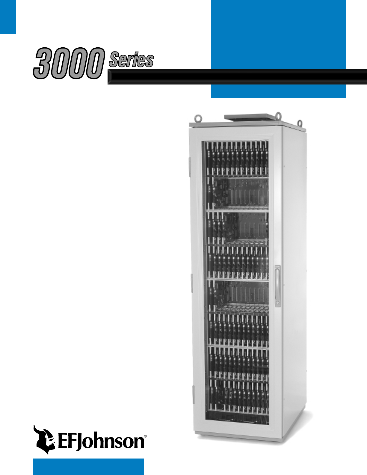
October 2003
Supersedes: Part No. 001-3139-003/004; 5/99
MULTI-NET®II
3000 S
ERIES
SWITCH
SET-UP AND
ALIGNMENT
SET-UP AND
ALIGNMENT
MULTI-NET®II SWITCH
Page 2

Page 3

MULTI-NET® II
3000 SERIES SWITCH
SETUP AND ALIGNMENT MANUAL
Copyright© 2003 by the EFJohnson Company
The EFJohnson Company, which was founded in 1923, provides wireless communication systems solutions for
public safety, government, and commercial customers. The company designs, manufactures, and markets conventional and trunked radio systems, mobile and portable subscriber radios, repeaters, and Project 25 digital radio
products. EFJohnson is a wholly owned subsidiary of EFJ, Inc.
Viking Head/EFJohnson logo, Multi-Net
other company and/or product names used in this manual are trademarks and/or registered trademarks of their
respective manufacturer.
Information in this manual is subject to change without notice. The EFJohnson Company will not be liable for any
misunderstanding due to misinformation or errors found in this document.
®
, and LTR®are registered trademarks of the EFJohnson Company. All
Page 4

SAFETY INFORMATION
The FCC has adopted a safety standard for human exposure to RF energy. Proper operation of this radio under
normal conditions results in user exposure to RF energy below the Occupational Safety and Health Act and Federal
Communication Commission limits.
WARNING
DO NOT allow the antenna to touch or come in very close proximity with the eyes, face, or any exposed body
parts while the radio is transmitting.
DO NOT allow the antenna to come close to or touch, the eyes, face, or any exposed body parts while the radio is
transmitting.
DO NOT operate the radio in explosive or flammable atmospheres. The transmitted radio energy could trigger
blasting caps or cause an explosion.
DO NOT operate the radio without the proper antenna installed.
DO NOT operate the radio unless all radio frequency connectors are secure and any open connectors are properly
terminated.
DO NOT allow children to operate or play with this equipment.
NOTE: The above warning list is not intended to include all hazards that may be encountered when using this
radio.
This device complies with Part 15 of the FCC rules. Operation is subject to the condition that this device does not
cause harmful interference. In addition, changes or modifications to this equipment not expressly approved by
EFJohnson could void the user’s authority to operate this equipment (FCC rules, 47CFR Part 15.19).
LAND MOBILE PRODUCT WARRANTY
The manufacturer’s warranty statement for this product is available from your product supplier or from EFJohnson
Company, 299 Johnson Avenue, Box 1249, Waseca, MN 56093-0514. Phone (507) 835-6222.
Page 5

TABLE OF CONTENTS
TABLE OF CONTENTS
1 INTRODUCTION
1.1 SCOPE OF MANUAL . . . . . . . . . . . . . . . . . . . 1-1
1.2 DEFINITIONS . . . . . . . . . . . . . . . . . . . . . . . . . . 1-1
Trunked System. . . . . . . . . . . . . . . . . . . . . . . . . . 1-1
LTR Trunked System . . . . . . . . . . . . . . . . . . . . . 1-1
Multi-Net Trunked System . . . . . . . . . . . . . . . . . 1-1
Conventional System. . . . . . . . . . . . . . . . . . . . . . 1-1
3000 Series Switch . . . . . . . . . . . . . . . . . . . . . . . 1-1
Call Processor . . . . . . . . . . . . . . . . . . . . . . . . . . . 1-1
System and Subscriber Manager . . . . . . . . . . . . . 1-1
Repeater Site . . . . . . . . . . . . . . . . . . . . . . . . . . . . 1-1
Home Repeater Channel . . . . . . . . . . . . . . . . . . . 1-1
Status Repeater Channel . . . . . . . . . . . . . . . . . . . 1-2
Monitor Repeater Channel. . . . . . . . . . . . . . . . . . 1-2
Telephone Interconnect and Data Transmission . 1-2
Public Switched Telephone Network (PSTN). . . 1-2
Private Automatic Branch Exchange (PABX) . . 1-2
2 3000 SERIES SWITCH
2.1 INTRODUCTION. . . . . . . . . . . . . . . . . . . . . . . . 2-1
2.2 ELEMENTS OF THE SWITCH. . . . . . . . . . . . 2-2
2.3 SWITCH MODULES (ELEMENTS). . . . . . . . 2-2
Voltage Adjustments . . . . . . . . . . . . . . . . . . . . . 4-8
Redundant Supply Adjustments. . . . . . . . . . . . . 4-8
Verify Fan Air Flow Direction. . . . . . . . . . . . . . 4-8
Verify Voltages On Power Distribution Cable . 4-8
System Test Procedure. . . . . . . . . . . . . . . . . . . . 4-9
Final Configuration Verification . . . . . . . . . . . 4-11
4.3 SIX SHELF 3000 SERIES SWITCH . . . . . . 4-13
Power Consumption. . . . . . . . . . . . . . . . . . . . . 4-13
Equipment Required . . . . . . . . . . . . . . . . . . . . 4-13
Verify Resistance of Bus Bar and Power Supply
Lines . . . . . . . . . . . . . . . . . . . . . . . . . . . . . . 4-14
Verify Cooling Fan Air Flow Direction. . . . . . 4-14
Verify Voltages On Power Distribution Cable 4-14
System Test Procedure. . . . . . . . . . . . . . . . . . . 4-14
Final Configuration Verification . . . . . . . . . . . 4-17
4.4 EIGHT SHELF 3000 SERIES SWITCH. . . . 4-20
Power Consumption. . . . . . . . . . . . . . . . . . . . . 4-20
Equipment Required . . . . . . . . . . . . . . . . . . . . 4-20
Verify Resistance of Bus Bar and Power
Supply Lines . . . . . . . . . . . . . . . . . . . . . . . . 4-20
Verify Cooling Fan Air Flow Direction. . . . . . 4-21
Verify Voltages On Power Distribution Cable 4-21
System Test Procedure. . . . . . . . . . . . . . . . . . . 4-21
Final Configuration Verification . . . . . . . . . . . 4-23
3 ARCHITECTURE
3.1 INTRODUCTION. . . . . . . . . . . . . . . . . . . . . . . . 3-1
3.2 SWITCH INTERFACES. . . . . . . . . . . . . . . . . . 3-1
3.3 BUS STRUCTURE. . . . . . . . . . . . . . . . . . . . . . 3-2
Data Bus. . . . . . . . . . . . . . . . . . . . . . . . . . . . . . . . 3-2
Control Bus . . . . . . . . . . . . . . . . . . . . . . . . . . . . . 3-3
Voice Bus. . . . . . . . . . . . . . . . . . . . . . . . . . . . . . . 3-4
4 SYSTEM RACK
4.1 TWO SHELF 3000 SERIES SWITCH. . . . . . 4-1
Power Consumption. . . . . . . . . . . . . . . . . . . . . . . 4-1
Equipment Required . . . . . . . . . . . . . . . . . . . . . . 4-1
Two Shelf Power Supply. . . . . . . . . . . . . . . . . . . 4-2
Power Supply Redundant Plate . . . . . . . . . . . . . . 4-2
Voltage Adjustments . . . . . . . . . . . . . . . . . . . . . . 4-2
Redundant Supply Adjustments . . . . . . . . . . . . . 4-2
Verify Fan Air Flow Direction . . . . . . . . . . . . . . 4-2
Verify Voltages on Power Distribution Cable. . . 4-3
System Test Procedure . . . . . . . . . . . . . . . . . . . . 4-3
Final Configuration Verification . . . . . . . . . . . . . 4-5
4.2 FOUR SHELF 3000 SERIES SWITCH. . . . . 4-7
Power Consumption. . . . . . . . . . . . . . . . . . . . . . . 4-7
Equipment Required . . . . . . . . . . . . . . . . . . . . . . 4-7
4-Shelf Power Supply . . . . . . . . . . . . . . . . . . . . . 4-7
Power Supply Redundant Plate . . . . . . . . . . . . . . 4-7
5 CALL PROCESSOR
5.1 INTRODUCTION. . . . . . . . . . . . . . . . . . . . . . . . 5-1
5.2 DATA BUSES . . . . . . . . . . . . . . . . . . . . . . . . . .5-1
5.3 CALL PROCESSOR CONTROL . . . . . . . . . . 5-2
System Configuration . . . . . . . . . . . . . . . . . . . . 5-2
Manual Device Control . . . . . . . . . . . . . . . . . . . 5-2
Subscriber Management. . . . . . . . . . . . . . . . . . . 5-2
Activity Log Utilities. . . . . . . . . . . . . . . . . . . . . 5-2
Call Completion. . . . . . . . . . . . . . . . . . . . . . . . . 5-2
Keyboard Lock. . . . . . . . . . . . . . . . . . . . . . . . . . 5-3
Log Out/Log In . . . . . . . . . . . . . . . . . . . . . . . . . 5-3
5.4 ALARM CONTROL . . . . . . . . . . . . . . . . . . . . . 5-3
5.5 SYSTEM ANALYZER . . . . . . . . . . . . . . . . . . .5-3
5.6 CALL PROCESSING . . . . . . . . . . . . . . . . . . . . 5-3
6 NETWORK INTERFACE MODULE
(NetNIM)
6.1 DESCRIPTION . . . . . . . . . . . . . . . . . . . . . . . . . 6-1
6.2 OPERATION . . . . . . . . . . . . . . . . . . . . . . . . . . . 6-1
LEDs . . . . . . . . . . . . . . . . . . . . . . . . . . . . . . . . . 6-2
6.3 SETUP PROCEDURE . . . . . . . . . . . . . . . . . . . 6-2
Jumpers . . . . . . . . . . . . . . . . . . . . . . . . . . . . . . . 6-2
Switches . . . . . . . . . . . . . . . . . . . . . . . . . . . . . . . 6-2
6.4 ALIGNMENT SPECIFICATIONS. . . . . . . . . .6-2
Detector Setting . . . . . . . . . . . . . . . . . . . . . . . . . 6-3
i
Page 6

TABLE OF CONTENTS (CONT’D)
TABLE OF CONTENTS
7 BASIC BOARD MODULE (BBM)
7.1 DESCRIPTION . . . . . . . . . . . . . . . . . . . . . . . . . 7-1
Main Audio . . . . . . . . . . . . . . . . . . . . . . . . . . . . . 7-1
Secondary Communication . . . . . . . . . . . . . . . . . 7-1
Internal Communication . . . . . . . . . . . . . . . . . . . 7-1
7.2 BBM SETUP PROCEDURE. . . . . . . . . . . . . . 7-3
Switch Settings . . . . . . . . . . . . . . . . . . . . . . . . . . 7-3
Jumper Placement . . . . . . . . . . . . . . . . . . . . . . . . 7-3
BBM Backplane External Connections. . . . . . . . 7-3
7.3 BBM ALIGNMENT PROCEDURES . . . . . . . 7-4
Introduction . . . . . . . . . . . . . . . . . . . . . . . . . . . . . 7-4
Alignment . . . . . . . . . . . . . . . . . . . . . . . . . . . . . . 7-4
7.4 TEST TASKS . . . . . . . . . . . . . . . . . . . . . . . . . . 7-5
System Switch Equals “1”. . . . . . . . . . . . . . . . . . 7-5
System Switch Equals “2”. . . . . . . . . . . . . . . . . . 7-5
System Switch Equals “3”. . . . . . . . . . . . . . . . . . 7-5
System Switch Equals “4”. . . . . . . . . . . . . . . . . . 7-5
System Switch Equals “5”. . . . . . . . . . . . . . . . . . 7-5
System Switch Equals “6”. . . . . . . . . . . . . . . . . . 7-5
System Switch Equals “7”. . . . . . . . . . . . . . . . . . 7-6
System Switch Equals “8”. . . . . . . . . . . . . . . . . . 7-6
System Switch Equals “9”. . . . . . . . . . . . . . . . . . 7-6
7.5 TROUBLESHOOTING. . . . . . . . . . . . . . . . . . . 7-6
Test “1” . . . . . . . . . . . . . . . . . . . . . . . . . . . . . . . . 7-6
Test “2” . . . . . . . . . . . . . . . . . . . . . . . . . . . . . . . . 7-7
Test “3” . . . . . . . . . . . . . . . . . . . . . . . . . . . . . . . . 7-7
Test “4” . . . . . . . . . . . . . . . . . . . . . . . . . . . . . . . . 7-7
Test “5” . . . . . . . . . . . . . . . . . . . . . . . . . . . . . . . . 7-8
Test “6” . . . . . . . . . . . . . . . . . . . . . . . . . . . . . . . . 7-9
Test “7” . . . . . . . . . . . . . . . . . . . . . . . . . . . . . . . . 7-9
Test “8” . . . . . . . . . . . . . . . . . . . . . . . . . . . . . . . . 7-9
Test “9” . . . . . . . . . . . . . . . . . . . . . . . . . . . . . . . . 7-9
7.6 DS1 DISPLAY DEFINITIONS. . . . . . . . . . . . . 7-9
8 CHANNEL INTERFACE MODULE
(CIM)
External Connections . . . . . . . . . . . . . . . . . . . . . 8-6
Alignment Procedure . . . . . . . . . . . . . . . . . . . . . 8-6
9 CONVENTIONAL CHANNEL MODULE
(CCM)
9.1 DESCRIPTION. . . . . . . . . . . . . . . . . . . . . . . . . .9-9
Repeater Signaling . . . . . . . . . . . . . . . . . . . . . . . 9-9
Repeater Control. . . . . . . . . . . . . . . . . . . . . . . . . 9-9
Voice Connection. . . . . . . . . . . . . . . . . . . . . . . . 9-9
Internal Communication. . . . . . . . . . . . . . . . . . . 9-9
9.2 CCM SETUP PROCEDURE . . . . . . . . . . . . . .9-9
CCM Switch Settings . . . . . . . . . . . . . . . . . . . . . 9-9
AFSK Communication on the Main Lines. . . . . 9-9
CCM Jumper Placement. . . . . . . . . . . . . . . . . . . 9-9
CCM Backplane External Contacts . . . . . . . . . 9-10
9.3 CCM ALIGNMENT SPECIFICATIONS . . . .9-10
Pre-Alignment . . . . . . . . . . . . . . . . . . . . . . . . . 9-10
CCM Alignment Procedure . . . . . . . . . . . . . . . 9-10
10 DISPATCH CHANNEL MODULE
(DCM)
10.1 DESCRIPTION. . . . . . . . . . . . . . . . . . . . . . . . .10-1
Repeater Signaling . . . . . . . . . . . . . . . . . . . . . . 10-1
Repeater Control. . . . . . . . . . . . . . . . . . . . . . . . 10-1
Voice Connection. . . . . . . . . . . . . . . . . . . . . . . 10-1
Internal Communication. . . . . . . . . . . . . . . . . . 10-1
10.2 DCM SETUP PROCEDURE . . . . . . . . . . . . .10-1
DCM Switch Settings. . . . . . . . . . . . . . . . . . . . 10-1
AFSK Communication on the Main Lines. . . . 10-1
DCM Jumper Placement. . . . . . . . . . . . . . . . . . 10-1
DCM Backplane External Contacts . . . . . . . . . 10-2
10.3 DCM ALIGNMENT SPECIFICATIONS . . . .10-2
Pre-Alignment . . . . . . . . . . . . . . . . . . . . . . . . . 10-2
DCM Alignment Procedure . . . . . . . . . . . . . . . 10-2
8.1 DESCRIPTION . . . . . . . . . . . . . . . . . . . . . . . . . 8-1
Repeater Signaling. . . . . . . . . . . . . . . . . . . . . . . . 8-1
Repeater Control . . . . . . . . . . . . . . . . . . . . . . . . . 8-1
Voice Connection . . . . . . . . . . . . . . . . . . . . . . . . 8-1
Internal Communication . . . . . . . . . . . . . . . . . . . 8-1
8.2 CIM SETUP PROCEDURE. . . . . . . . . . . . . . . 8-1
Switch Settings . . . . . . . . . . . . . . . . . . . . . . . . . . 8-1
Jumper Placement . . . . . . . . . . . . . . . . . . . . . . . . 8-2
CIM Backplane External Contacts . . . . . . . . . . . 8-2
External Connections. . . . . . . . . . . . . . . . . . . . . . 8-4
8.3 CIM ALIGNMENT SPECIFICATIONS . . . . . 8-4
Pre-Alignment . . . . . . . . . . . . . . . . . . . . . . . . . . . 8-4
CIM Alignment Procedure . . . . . . . . . . . . . . . . . 8-4
8.4 CIM AUDIO SUMMATION PERSONALITY
CARD. . . . . . . . . . . . . . . . . . . . . . . . . . . . . . . . 8-6
Internal Connections . . . . . . . . . . . . . . . . . . . . . . 8-6
11 DISPATCH INTERFACE MODULE
(DIM)
11.1 DESCRIPTION. . . . . . . . . . . . . . . . . . . . . . . . .11-1
11.2 DIM SETUP PROCEDUR E . . . . . . . . . . . . . .11-1
Switch Settings. . . . . . . . . . . . . . . . . . . . . . . . . 11-1
DIM Jumper Placement . . . . . . . . . . . . . . . . . . 11-1
E-Lead Selection. . . . . . . . . . . . . . . . . . . . . . . . 11-2
DIM Backplane External Contacts. . . . . . . . . . 11-2
11.3 DIM ALIGNMENT SPECIFICATION . . . . . .11-2
Pre-Alignment . . . . . . . . . . . . . . . . . . . . . . . . . 11-2
Pre-Alignment With Tone Remote Personality
Card . . . . . . . . . . . . . . . . . . . . . . . . . . . . . . . 11-2
11.4 ALIGNMENT . . . . . . . . . . . . . . . . . . . . . . . . . .11-3
11.5 TONE REMOTE DTMF OPERATION . . . . .11-4
ii
Page 7

TABLE OF CONTENTS (CONT’D)
TABLE OF CONTENTS
12 INTELLIGENT DISPATCH MODULE
(IDM)
12.1 DESCRIPTION . . . . . . . . . . . . . . . . . . . . . . . . 12-1
12.2 IDM SETUP PROCEDURE. . . . . . . . . . . . . . 12-2
Switch Settings . . . . . . . . . . . . . . . . . . . . . . . . . 12-2
IDM Jumper Placement. . . . . . . . . . . . . . . . . . . 12-2
IDM Backplane External Contacts . . . . . . . . . . 12-2
12.3 IDM ALIGNMENT SPECIFICATION. . . . . . 12-4
Pre-Alignment . . . . . . . . . . . . . . . . . . . . . . . . . . 12-4
12.4 ALIGNMENT . . . . . . . . . . . . . . . . . . . . . . . . . . 12-4
12.5 PCM SUMMATION PERSONALITY CARD12-5
Internal Connections . . . . . . . . . . . . . . . . . . . . . 12-5
External Connections. . . . . . . . . . . . . . . . . . . . . 12-5
Alignment Procedure. . . . . . . . . . . . . . . . . . . . . 12-5
13 SYSTEM NETWORK MODULE (SNM)
13.1 DESCRIPTION . . . . . . . . . . . . . . . . . . . . . . . . 13-1
13.2 SNM SETUP PROCEDURE. . . . . . . . . . . . . 13-2
SNM Switch Settings. . . . . . . . . . . . . . . . . . . . . 13-2
AFSK Communication on the Main Lines . . . . 13-2
SNM Jumper Placement . . . . . . . . . . . . . . . . . . 13-2
SNM Backplane External Contacts . . . . . . . . . . 13-2
13.3 SNM ALIGNMENT SPECIFICATIONS. . . . 13-2
Pre-Alignment . . . . . . . . . . . . . . . . . . . . . . . . . . 13-2
SNM Alignment Procedure . . . . . . . . . . . . . . . . 13-2
14 TELEPHONE INTERFACE MODULE
(TIM)
14.1 DESCRIPTION . . . . . . . . . . . . . . . . . . . . . . . . 14-1
Supervision . . . . . . . . . . . . . . . . . . . . . . . . . . . . 14-2
Signaling . . . . . . . . . . . . . . . . . . . . . . . . . . . . . . 14-2
Call Supervision. . . . . . . . . . . . . . . . . . . . . . . . . 14-2
Intra-terminal Communication . . . . . . . . . . . . . 14-2
Telephone Line Styles . . . . . . . . . . . . . . . . . . . . 14-3
Audio Processing. . . . . . . . . . . . . . . . . . . . . . . . 14-3
Receive Audio . . . . . . . . . . . . . . . . . . . . . . . . . . 14-3
Transmit Audio . . . . . . . . . . . . . . . . . . . . . . . . . 14-4
14.2 4-WIRE E&M INTERFACE DESCRIPTION14-4
Audio . . . . . . . . . . . . . . . . . . . . . . . . . . . . . . . . . 14-4
E&M Leads . . . . . . . . . . . . . . . . . . . . . . . . . . . . 14-4
8-position Dip Switch S201. . . . . . . . . . . . . . . . 14-5
Type I and V . . . . . . . . . . . . . . . . . . . . . . . . . . . 14-6
Type II and III . . . . . . . . . . . . . . . . . . . . . . . . . . 14-6
Type IV . . . . . . . . . . . . . . . . . . . . . . . . . . . . . . . 14-6
Type II Trunk-To-Trunk . . . . . . . . . . . . . . . . . . 14-6
Type V Trunk-to-Trunk. . . . . . . . . . . . . . . . . . . 14-7
14.3 LED STATUS FOR E&M LEADS. . . . . . . . .14-7
TELCO Side Status . . . . . . . . . . . . . . . . . . . . . 14-7
E&M Logic Status . . . . . . . . . . . . . . . . . . . . . . 14-7
14.4 E&M LEAD CIRCUIT THEORY OF
OPERATION . . . . . . . . . . . . . . . . . . . . . . . . .14-8
E&M Interface . . . . . . . . . . . . . . . . . . . . . . . . . 14-8
Signal Conditioning . . . . . . . . . . . . . . . . . . . . . 14-8
14.5 TIM SETUP PROCEDURE . . . . . . . . . . . . .14-11
TIM Jumper Placement . . . . . . . . . . . . . . . . . 14-11
Main Board Switch Settings. . . . . . . . . . . . . . 14-11
14.6 2WY SETUP AND ALIGNMENT
PROCEDURES (-670). . . . . . . . . . . . . . . .14-11
2WY Jumper Setup. . . . . . . . . . . . . . . . . . . . . 14-11
2WY Pre-Alignment Procedures . . . . . . . . . . 14-11
14.7 2-WAY TIM ALIGNMENT
PROCEDURES (-670). . . . . . . . . . . . . . . .14-13
Main Receive . . . . . . . . . . . . . . . . . . . . . . . . . 14-13
Dial Tone Detector . . . . . . . . . . . . . . . . . . . . . 14-13
Output Hybrid Adjust. . . . . . . . . . . . . . . . . . . 14-14
14.8 DID SETUP AND ALIGNMENT (-660) . . .14-15
DID Personality Card Jumper Settings. . . . . . 14-15
Pre-Alignment . . . . . . . . . . . . . . . . . . . . . . . . 14-15
14.9 DID OPERATIONAL ALIGNMENT
PROCEDURES (-660). . . . . . . . . . . . . . . .14-16
14.10 E&M SETUP AND ALIGNMENT (-680) . .14-17
Equipment Required. . . . . . . . . . . . . . . . . . . . 14-17
Transmit Alignment . . . . . . . . . . . . . . . . . . . . 14-17
Receiver Alignment . . . . . . . . . . . . . . . . . . . . 14-18
4-Wire E&M Dial Tone Detector Receive
Alignment. . . . . . . . . . . . . . . . . . . . . . . . . . 14-18
14.11 TERMSET MODULES . . . . . . . . . . . . . . . . .14-23
Equipment Setup. . . . . . . . . . . . . . . . . . . . . . . 14-23
Initializing the Tellabs Cards . . . . . . . . . . . . . 14-23
Switch Settings On 6132A (DID
Applications) . . . . . . . . . . . . . . . . . . . . . . . 14-24
XEL Termset Rack. . . . . . . . . . . . . . . . . . . . . 14-25
Connection To the Phone Lines . . . . . . . . . . . 14-26
Final Path Inspection . . . . . . . . . . . . . . . . . . . 14-27
14.12 BACKGROUND INFORMATION . . . . . . . .14-27
Standard Signal. . . . . . . . . . . . . . . . . . . . . . . . 14-27
Outlined Objective . . . . . . . . . . . . . . . . . . . . . 14-27
The Order of Things. . . . . . . . . . . . . . . . . . . . 14-27
14.13 TUNING A DOD OR DID 2-WIRE INTERFACE
TO THE 4-WIRE E&M BOARD.. . . . . . . .14-28
14.14 BALANCING TO THE CENTRAL
OFFICE. . . . . . . . . . . . . . . . . . . . . . . . . . . . .14-30
Introduction . . . . . . . . . . . . . . . . . . . . . . . . . . 14-30
Statistics . . . . . . . . . . . . . . . . . . . . . . . . . . . . . 14-30
Adding Capacitance to the Termset . . . . . . . . 14-30
Rural Areas. . . . . . . . . . . . . . . . . . . . . . . . . . . 14-30
Urban Areas . . . . . . . . . . . . . . . . . . . . . . . . . . 14-30
14.15 FCC USER INSTRUCTIONS AND
CUSTOMER INFORMATION. . . . . . . . . .14-31
iii
Page 8

TABLE OF CONTENTS (CONT’D)
TABLE OF CONTENTS
15 VOTER DIAGNOSTICS MODULE
(VDM)
15.1 DESCRIPTION . . . . . . . . . . . . . . . . . . . . . . . . 15-1
15.2 VDM SETUP PROCEDURE . . . . . . . . . . . . . 15-1
Switch Settings . . . . . . . . . . . . . . . . . . . . . . . . . 15-1
Jumper Placement . . . . . . . . . . . . . . . . . . . . . . . 15-2
VDM Backplane External Contacts. . . . . . . . . . 15-2
15.3 VDM ALIGNMENT SPECIFICATIONS. . . . 15-2
16 POWER TERMINATION MODULE
(PTM)
16.1 DESCRIPTION . . . . . . . . . . . . . . . . . . . . . . . . 16-1
16.2 SETUP PROCEDURE . . . . . . . . . . . . . . . . . . 16-1
17 LOGGING ENCODER MODULE (LEM)
17.1 DESCRIPTION . . . . . . . . . . . . . . . . . . . . . . . . 17-1
17.2 LEM SETUP PROCEDURE . . . . . . . . . . . . . 17-2
LEM Switch Settings. . . . . . . . . . . . . . . . . . . . . 17-2
LEM Jumper Placement . . . . . . . . . . . . . . . . . . 17-2
LEM Backplane External Contacts . . . . . . . . . . 17-2
17.3 LEM ALIGNMENT SPECIFICATIONS . . . . 17-2
Pre-Alignment . . . . . . . . . . . . . . . . . . . . . . . . . . 17-2
LEM Alignment Procedure . . . . . . . . . . . . . . . . 17-2
18 VOICE TONE MODULE (VTM)
18.1 DESCRIPTION . . . . . . . . . . . . . . . . . . . . . . . . 18-1
18.2 SETUP PROCEDURE . . . . . . . . . . . . . . . . . . 18-1
VTM Jumper Placement . . . . . . . . . . . . . . . . . . 18-1
VTM Switch Settings . . . . . . . . . . . . . . . . . . . . 18-1
18.3 ALIGNMENT SPECIFICATIONS. . . . . . . . . 18-1
20 MULTI-NET CONSOLE MODULE
(MCM)
20.1 DESCRIPTION. . . . . . . . . . . . . . . . . . . . . . . . .20-1
20.2 MCM SETUP PROCEDURE . . . . . . . . . . . . . 20-2
Switch Settings. . . . . . . . . . . . . . . . . . . . . . . . . 20-2
MCM Jumper Placement . . . . . . . . . . . . . . . . . 20-2
MCM Backplane External Contacts. . . . . . . . . 20-2
20.3 MCM ALIGNMENT SPECIFICATION . . . . .20-2
Pre-Alignment . . . . . . . . . . . . . . . . . . . . . . . . . 20-2
20.4 ALIGNMENT . . . . . . . . . . . . . . . . . . . . . . . . . .20-3
20.5 PCM SUMMATION PERSONALITY CARD20-4
Internal Connections. . . . . . . . . . . . . . . . . . . . . 20-4
External Connections . . . . . . . . . . . . . . . . . . . . 20-4
Alignment Procedure . . . . . . . . . . . . . . . . . . . . 20-4
21 CONVENTIONAL PATCH MODULE
(CPM)
21.1 DESCRIPTION. . . . . . . . . . . . . . . . . . . . . . . . .21-1
21.2 PCM SETUP PROCEDURE . . . . . . . . . . . . .21-1
Switch Settings. . . . . . . . . . . . . . . . . . . . . . . . . 21-1
CPM Jumper Placement . . . . . . . . . . . . . . . . . . 21-1
E-Lead Selection. . . . . . . . . . . . . . . . . . . . . . . . 21-2
CPM Backplane External Contacts . . . . . . . . . 21-2
21.3 CPM ALIGNMENT SPECIFICATION . . . . .21-2
Pre-Alignment . . . . . . . . . . . . . . . . . . . . . . . . . 21-2
Alignment. . . . . . . . . . . . . . . . . . . . . . . . . . . . . 21-2
22 POWER SUPPLY
19 WIDE AREA MODULE (WAM)
19.1 DESCRIPTION . . . . . . . . . . . . . . . . . . . . . . . . 19-1
19.2 WAM SETUP PROCEDURE . . . . . . . . . . . . 19-2
WAM Switch Settings. . . . . . . . . . . . . . . . . . . . 19-2
WAM Jumper Placement. . . . . . . . . . . . . . . . . . 19-2
WAM Backplane External Contacts . . . . . . . . . 19-2
19.3 WAM ALIGNMENT SPECIFICATIONS . . . 19-2
Pre-Alignment . . . . . . . . . . . . . . . . . . . . . . . . . . 19-2
WAM Alignment Procedure . . . . . . . . . . . . . . . 19-2
19.4 WAM E&M-LEAD CONNECTIONS . . . . . . 19-4
One Location . . . . . . . . . . . . . . . . . . . . . . . . . . . 19-5
Two Locations . . . . . . . . . . . . . . . . . . . . . . . . . . 19-5
Three Locations . . . . . . . . . . . . . . . . . . . . . . . . . 19-5
19.5 M-LEAD SPLITTER BOX . . . . . . . . . . . . . . . 19-5
General. . . . . . . . . . . . . . . . . . . . . . . . . . . . . . . . 19-5
Installation . . . . . . . . . . . . . . . . . . . . . . . . . . . . . 19-5
19.6 WAM AUDIO CONNECTIONS. . . . . . . . . . . 19-6
22.1 INTRODUCTION . . . . . . . . . . . . . . . . . . . . . . . 22-1
22.2 POWER CONSUMPTION . . . . . . . . . . . . . . .22-1
23 BACKPLANE
23.1 DESCRIPTION. . . . . . . . . . . . . . . . . . . . . . . . .23-1
23.2 BACKPLANE SETUP PROCEDURE . . . . .23-1
Shelf Address Settings . . . . . . . . . . . . . . . . . . . 23-1
Termination Settings. . . . . . . . . . . . . . . . . . . . . 23-1
Jumper Definitions and Settings. . . . . . . . . . . . 23-1
23.3 STANDARD SHELF I/O CONNECTIONS .23-2
23.4 CIM SHELF I/O CONNECTIONS . . . . . . . . .23-3
Primary PCM . . . . . . . . . . . . . . . . . . . . . . . . . . 23-3
Secondary PCM . . . . . . . . . . . . . . . . . . . . . . . . 23-3
23.5 NetNIM SHELF WITH CIM/CCMs . . . . . . . .23-4
23.6 NetNIM SHELF WITHOUT CIM/CCMs . . . .23-5
iv
Page 9

TABLE OF CONTENTS (CONT’D)
TABLE OF CONTENTS
24 INTERCOM
24.1 DESCRIPTION . . . . . . . . . . . . . . . . . . . . . . . . 24-1
24.2 INSTALLATION . . . . . . . . . . . . . . . . . . . . . . . 24-1
Equipment Required . . . . . . . . . . . . . . . . . . . . . 24-1
Installation Procedure . . . . . . . . . . . . . . . . . . . . 24-1
APPENDIX A ERROR MESSAGES
A.1 IDB Error Messages To Message
Accounting Bus From Modules. . . . . . . .A-1
A.2 MAB Error Messages From System
Management Module. . . . . . . . . . . . . . . . . .A-2
APPENDIX B CALL SEQUENCES
B.1 GROUP CALL. . . . . . . . . . . . . . . . . . . . . . . . . . B-1
Mobile To Mobile On Same Site. . . . . . . . . . . . B-1
Mobile To Mobile With DIM Monitoring. . . . . B-1
B.2 Dispatch Console (DC) To Mobile Group
Call . . . . . . . . . . . . . . . . . . . . . . . . . . . . . . . . . B-1
B.3 Mobile Group Call To Dispatch Console. B-1
B.4 Mobile To Unique ID . . . . . . . . . . . . . . . . . . . B-2
B.5 Mobile To Unique ID For a Mobile Outside
Switch . . . . . . . . . . . . . . . . . . . . . . . . . . . . . . B-3
B.6 Mobile To Directed Group Call (DTMF
Entry Within Switch) . . . . . . . . . . . . . . . . . B-3
B.7 Mobile To Directed Group Call (DTMF
Entry Outside the Switch)B-4
B.8 Mobile Originated Telephone Call. . . . . . . B-5
B.9 Landside (TIM) Originate To Mobile
Within Switch Using a DID Line . . . . . . . B-6
B.10 Landside (TIM) Originate To Mobile
Within Switch Using a 2WY Line . . . . . . B-6
B.11 TIM Originate To Mobile Outside Switch
Using a DID Line . . . . . . . . . . . . . . . . . . . . . B-7
B.12 Landside Originate To Mobile Outside
Switch Using a 2WY Line . . . . . . . . . . . . . B-7
LIST OF FIGURES
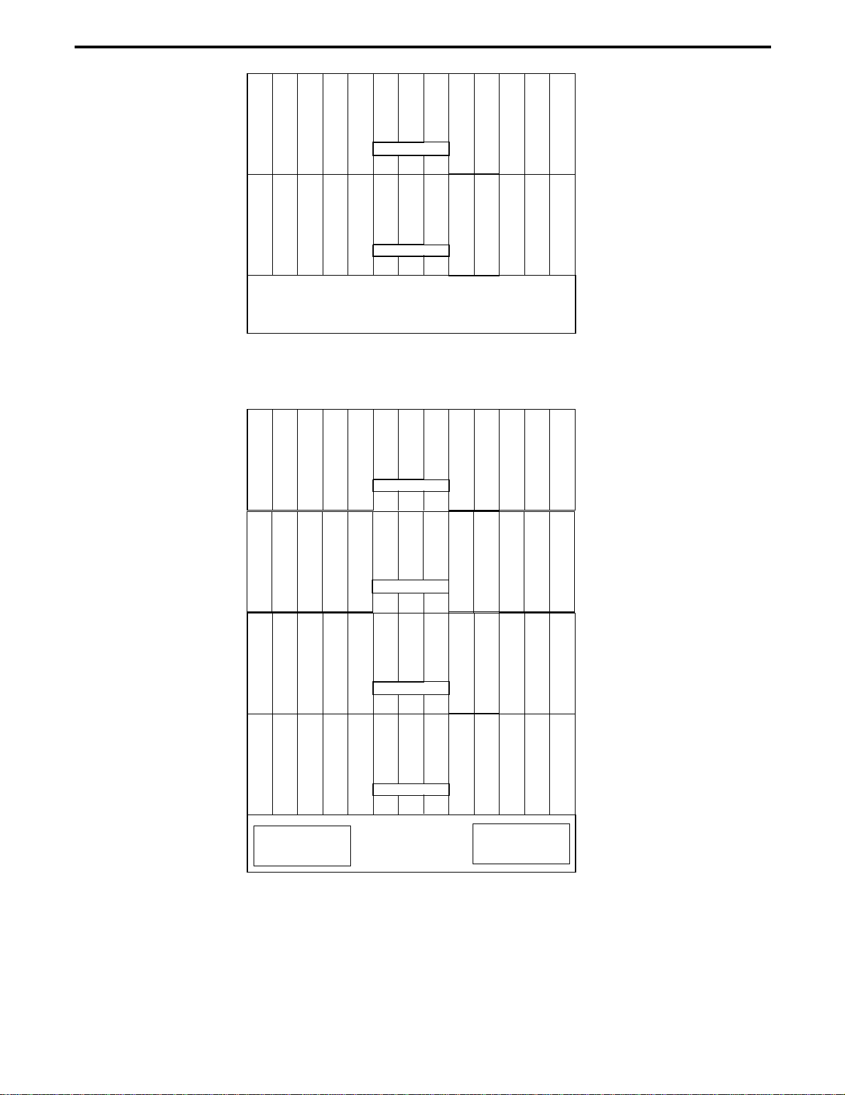
2-1 2-Shelf 3000 Series Switch . . . . . . . . . . . . . . . . 2-3
2-2 4-Shelf 3000 Series Switch . . . . . . . . . . . . . . . . 2-3
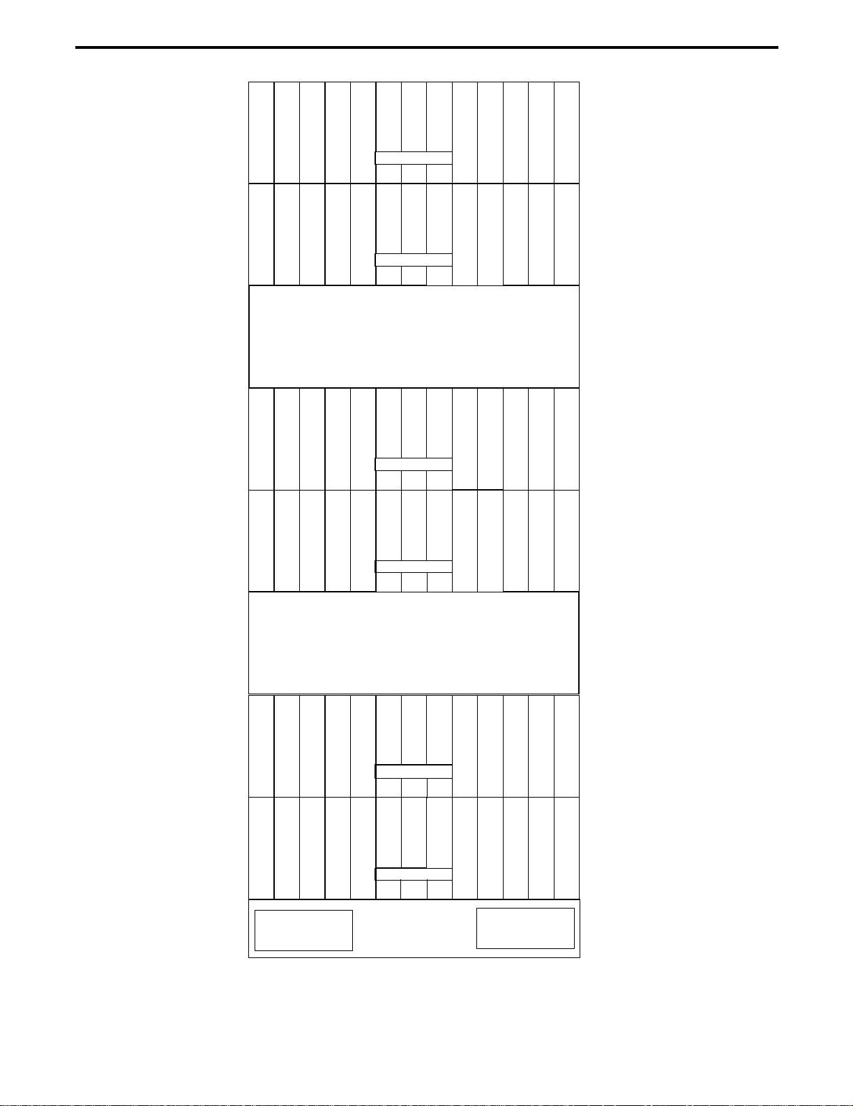
2-3 6-Shelf Switch Rack Layout . . . . . . . . . . . . . . . 2-4
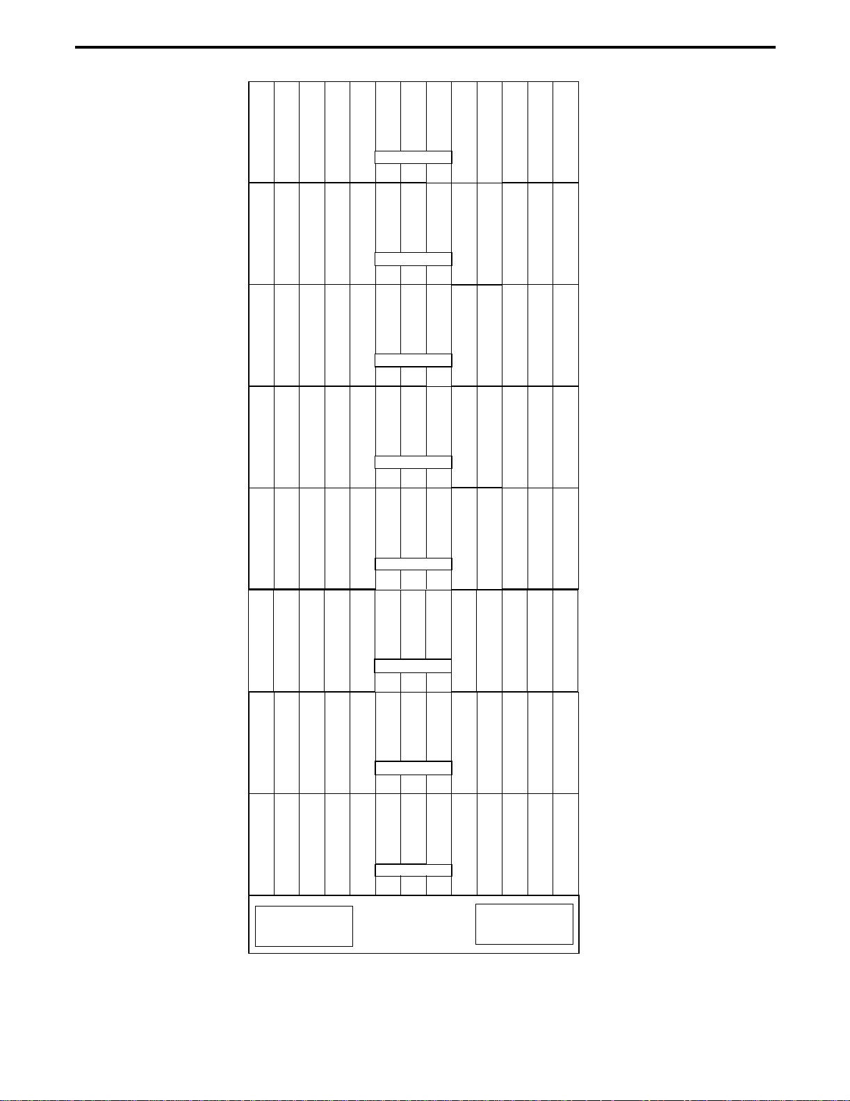
2-4 8-Shelf Switch Rack Setup . . . . . . . . . . . . . . . . 2-5
3-1 Multi-Net System Switch . . . . . . . . . . . . . . . . . 3-1
3-2 Data Buses . . . . . . . . . . . . . . . . . . . . . . . . . . . . . 3-2
3-3 Control Buses. . . . . . . . . . . . . . . . . . . . . . . . . . . 3-3
3-4 Voice Buses . . . . . . . . . . . . . . . . . . . . . . . . . . . . 3-4
4-1 2-shelf 30 00 Series Switch Backplane Cables. . 4-6
4-2 2-shelf 3000 Series Switch Setup . . . . . . . . . . . 4-6
4-3 4-shelf 30 00 Series Switch Backplane Cables. 4-12
4-4 4-shelf 3000 Series Switch Setup . . . . . . . . . . 4-12
4-5 Six Shelf 3000 Series Switch Backplane Cables 4-18
4-6 Six Shelf 3000 Series Switch Setup. . . . . . . . . 4-19
4-7 Eight Shelf 300 0 Series Sw Backplane Cables 4-25
4-8 8-Shelf 3000 Series Switch Rack Setup . . . . . 4-26
4-9 2- 4 Shelf Power Supply Interconnect . . . . . . . 4-27
4-10 6-8 Shelf Power Supp ly Interconnect Diagram 4-28
5-1 Data Buses . . . . . . . . . . . . . . . . . . . . . . . . . . . . . 5-1
6-1 Data Bus Block Diagram . . . . . . . . . . . . . . . . . . 6-1
6-2 NetNIM Card Edge Layout . . . . . . . . . . . . . . . . 6-3
6-3 NetNIM Alignment Points Diagram . . . . . . . . . 6-4
7-1 Basic Board Module Block Di agram . . . . . . . . . 7-2
7-2 Basic Board Module Alig n Poi nts Diagram. . . 7-12
7-3 Basic Board Module Card Edge Layou t. . . . . . 7-13
8-1 Alignment Points Diagram . . . . . . . . . . . . . . . . . 8-3
8-2 CIM Input and Output Levels. . . . . . . . . . . . . . . 8-5
8-3 Summati on Board Alignment Points Diagram. . 8-7
9-1 Alignment Points Diagram . . . . . . . . . . . . . . . . 9-11
10-1 Alignment Points Diagram . . . . . . . . . . . . . . . . 10-3
11-1 Alignment Points Diagram . . . . . . . . . . . . . . . . 11-5
11-2 PTT Tone Remote Card Block Diag ram . . . . . 11-6
11-3 PTT Tone Remote Card Align ment Points Diag 11-7
12-1 IDM Data Bus. . . . . . . . . . . . . . . . . . . . . . . . . . 12-1
12-2 Alignment Points Diagram . . . . . . . . . . . . . . . . 12-3
12-3 Summation Board Alignment Points Diagram. 12-6
13-1 Data Bus Block Diagram . . . . . . . . . . . . . . . . . 13-1
13-2 Alignment Points Diagram . . . . . . . . . . . . . . . . 13-3
13-3 SNM Cable Layout. . . . . . . . . . . . . . . . . . . . . . 13-4
14-1 Data Buses . . . . . . . . . . . . . . . . . . . . . . . . . . . . 14-1
14-2 E&M Interface Connections. . . . . . . . . . . . . . . 14-5
14-3 S201 . . . . . . . . . . . . . . . . . . . . . . . . . . . . . . . . . 14-5
14-4 TYPE I and V . . . . . . . . . . . . . . . . . . . . . . . . . . 14-6
14-5 TYPE II and III. . . . . . . . . . . . . . . . . . . . . . . . . 14-6
v
Page 10

LIST OF FIGURES (CONT’D)
TABLE OF CONTENTS
14-6 TYPE IV . . . . . . . . . . . . . . . . . . . . . . . . . . . . . 14-6
14-7 TYPE II Trunk-Trunk . . . . . . . . . . . . . . . . . . . 14-7
14-8 TYPE IV Trunk-Trunk . . . . . . . . . . . . . . . . . . 14-7
14-9 E&M Personality Board . . . . . . . . . . . . . . . . . 14-7
14-10 Main Board . . . . . . . . . . . . . . . . . . . . . . . . . . . 14-7
14-11 Type III Interface. . . . . . . . . . . . . . . . . . . . . . . 14-8
14-12 Charging Characteristic of C227. . . . . . . . . . . 14-8
14-13 4-Wire E&M Block Diagram (-680) . . . . . . . . 14-9
14-14 DT & MBS Personality Card Blk Diag (-670) 14-10
14-15 DID Personality Card Block Diagram (-660) 14-10
14-16 Transmit Diagram . . . . . . . . . . . . . . . . . . . . . 14-18
14-17 Receive Diagram . . . . . . . . . . . . . . . . . . . . . . 14-18
14-18 Alignment Points Diagram . . . . . . . . . . . . . . 14-19
14-19 DT & MBS Alignment Points Diagram (-670) 14-20
14-20 DID Alignment Points Diagram (-660) . . . . . 14-21
14-21 4-Wire E&M Alignment Points Diag (-680) . 14-22
14-22 TELLABS 6132B - POTS. . . . . . . . . . . . . . . 14-23
14-23 TELLABS 6132A - DID . . . . . . . . . . . . . . . . 14-24
14-24 XEL Termset Rack (Rear Close-up) . . . . . . . 14-25
14-25 Termset Rack (Front View). . . . . . . . . . . . . . 14-26
14-26 Network Link (Switch Rack Back View) . . . 14-26
14-27 E&M Interface. . . . . . . . . . . . . . . . . . . . . . . . 14-28
14-28 Tellabs 6132A/B Termset . . . . . . . . . . . . . . . 14-29
14-29 6132 Tellabs Card . . . . . . . . . . . . . . . . . . . . . 14-31
15-1 Data Buses . . . . . . . . . . . . . . . . . . . . . . . . . . . . 15-1
15-2 VDM Connections . . . . . . . . . . . . . . . . . . . . . . 15-2
15-3 Alignment Points Diagram . . . . . . . . . . . . . . . 15-3
16-1 Power Terminat ion Mod Align Points Diag . . 16-2
17-1 Data Bus Block Diagram. . . . . . . . . . . . . . . . . 17-1
17-2 Alignment Points Diagram . . . . . . . . . . . . . . . 17-4
18-1 Voice Buses . . . . . . . . . . . . . . . . . . . . . . . . . . . 18-2
18-2 VTM Card Edge Layout . . . . . . . . . . . . . . . . . 18-3
19-1 Data Bus Block Diagram. . . . . . . . . . . . . . . . . 19-1
19-2 Alignment Points Diagram . . . . . . . . . . . . . . . 19-3
19-3 WAM E&M Lead Cable Layout 1 Location. . 19-4
19-4 WAM E&M Lead Cable Layout 2 Locations . 19-5
19-5 M-Lead Splitter Box I/Os . . . . . . . . . . . . . . . . 19-5
19-6 WAM E&M Lead Cable Layout 3 Locations . 19-6
19-7 WAM Audio Cable Layout One Location. . . . 19-6
19-8 WAM Audio Cable Layout Two Locations . . 19-6
19-9 Audio Cabl e Lay. Tw o Loc. w/Ext Audio Dev 19-7
19-10 Audio Cable Lay. Host Loc. 3 Location Config 19-7
20-1 Data Bus Block Diagram . . . . . . . . . . . . . . . . . 20-1
20-2 Alignment Points Diagram . . . . . . . . . . . . . . . . 20-5
20-3 Summati on Board (-760 ) Align Points Diagram 20-6
21-1 CPM Alignm ent Points Diagram . . . . . . . . . . . 21-3
22-1 Power Supply . . . . . . . . . . . . . . . . . . . . . . . . . . 22-1
22-2 6-8 Shelf Power Supply In terconnect Diagram 22-2
22-3 A3-A4 Connector . . . . . . . . . . . . . . . . . . . . . . . 22-3
22-4 A5-A6 Connector . . . . . . . . . . . . . . . . . . . . . . . 22-3
22-5 Power Supply Terminal Blocks . . . . . . . . . . . . 22-3
22-6 Power Supply Drawer. . . . . . . . . . . . . . . . . . . . 22-4
22-7 2-4 Shelf Power Supply In terconnect. . . . . . . . 22-5
22-8 2-4 Shelf Power Supply (Front View) . . . . . . . 22-6
22-9 2-4 Shelf Power Supply (R ear View) . . . . . . . . 22-6
23-1 Std Shelf Backplane Sw and Jumper Set tings . 23-2
23-2 S2 - S8 Switch Settings . . . . . . . . . . . . . . . . . . 23-3
23-3 CIM/CCM Shelf Backplane Sw & Jmpr Set.. . 23-3
23-4 NetNIM Shelf w/CIM/CCMs Sw & Jmpr Set.. 23-4
23-5 NetNIM Shelf w/o CIM/CCMs Sw & Jmpr Set. 23-5
23-6 2-Shelf 3000 Series Switch. . . . . . . . . . . . . . . . 23-6
23-7 4-Shelf 3000 Series Switch. . . . . . . . . . . . . . . . 23-6
23-8 6-Shelf Switch Rack Layout. . . . . . . . . . . . . . . 23-7
23-9 8-Shelf Switch Rack Setup. . . . . . . . . . . . . . . . 23-8
23-10 2-Shelf Switch Backplane Cables. . . . . . . . . . . 23-9
23-11 4-Shelf Switch Backplane Cables. . . . . . . . . . . 23-9
23-12 6-Shelf Switch Backplane Cables. . . . . . . . . . 23-10
23-13 8-Shelf Switch Backplane Cables. . . . . . . . . . 23-11
23-14 Basic Board Backplane Wiring Layout . . . . . 23-12
23-15 NetNIM Shelf Backplane Wiring Layout. . . . 23-12
23-16 Telephone Terminal Block Layout. . . . . . . . . 23-13
23-17 Backplane I/O Jacks . . . . . . . . . . . . . . . . . . . . 23-14
B-1 SNM Unique ID Request Flowchart . . . . . . . . B-8
B-2 DIM Unique ID Request Flowchart . . . . . . . . . B-9
B-3 CIM DTMF Auxiliary Call Flowchart . . . . . . . B-9
B-4 Dialed Digits and Number of Digits Flowch art B-10
B-5 Telephone TIM Incoming Flowchart . . . . . . . B-11
B-6 Telephone Calling CIM Call Req Flowchart . B-12
B-7 Dynamic Reass User Interface Req Flowchart B-13
B-8 Selective Unit Dis User Interface Req Flow . B-13
vi
Page 11

LIST OF TABLES
TABLE OF CONTENTS
2-1 Switch Modules . . . . . . . . . . . . . . . . . . . . . . . . . 2-2
4-1 Average Voltage/Current/Power . . . . . . . . . . . . 4-1
4-2 Power Supply Connections . . . . . . . . . . . . . . . . . 4-2
4-3 Power Distribution Cable Voltages . . . . . . . . . . 4-3
4-4 PCM Cable Location . . . . . . . . . . . . . . . . . . . . . 4-3
4-5 S1 Switch Settings . . . . . . . . . . . . . . . . . . . . . . . 4-4
4-6 Average Voltage/current/power . . . . . . . . . . . . . 4-7
4-7 Power Supply Connections . . . . . . . . . . . . . . . . . 4-8
4-9 PCM Cable Location . . . . . . . . . . . . . . . . . . . . . 4-9
4-8 Power Distribution Cable Voltages . . . . . . . . . . 4-9
4-10 S1 Switch Settings . . . . . . . . . . . . . . . . . . . . . . . 4-9
4-11 Average Voltage/Current/Power . . . . . . . . . . . 4-13
4-12 Bus Bar Resistance . . . . . . . . . . . . . . . . . . . . . . 4-13
4-13 Power Distribution Cable Voltages . . . . . . . . . 4-14
4-15 S1 Switch Settings . . . . . . . . . . . . . . . . . . . . . . 4-15
4-14 PCM Cable Location . . . . . . . . . . . . . . . . . . . . 4-15
4-16 Average Voltage/Current/Power . . . . . . . . . . . 4-20
4-17 Bus Bar Resistance . . . . . . . . . . . . . . . . . . . . . . 4-20
4-18 Power Distribution Cable Voltages . . . . . . . . . 4-21
4-19 PCM Cable Location . . . . . . . . . . . . . . . . . . . . 4-21
4-20 S1 Switch Settings . . . . . . . . . . . . . . . . . . . . . . 4-22
6-1 NIM Jumpers . . . . . . . . . . . . . . . . . . . . . . . . . . . 6-2
7-1 Basic Board Switch Settings . . . . . . . . . . . . . . . . 7-3
7-2 Basic Board Jumper Placement . . . . . . . . . . . . . 7-3
7-3 Backplane Pin-outs . . . . . . . . . . . . . . . . . . . . . . . 7-3
7-4 DIM Card Display/tasks . . . . . . . . . . . . . . . . . . . 7-9
7-5 CCM Card Display Tasks . . . . . . . . . . . . . . . . . . 7-9
7-6 CIM Card Display/tasks . . . . . . . . . . . . . . . . . . 7-10
7-7 TIM Card Display/tasks . . . . . . . . . . . . . . . . . . 7-10
7-9 DCM Card Display/tasks . . . . . . . . . . . . . . . . . 7-10
7-8 SNM Card Display/tasks . . . . . . . . . . . . . . . . . 7-10
7-11 LEM Card Display/tasks . . . . . . . . . . . . . . . . . . 7-11
7-12 GPM Card Display/tasks . . . . . . . . . . . . . . . . . 7-11
7-13 VDM Card Display/tasks . . . . . . . . . . . . . . . . . 7-11
7-10 IDM Card Display/tasks . . . . . . . . . . . . . . . . . . 7-11
7-14 WAM Card Display/tasks . . . . . . . . . . . . . . . . . 7-11
8-1 CIM Switch Settings . . . . . . . . . . . . . . . . . . . . . . 8-2
8-2 CIM Board Jumper Placement . . . . . . . . . . . . . . 8-2
8-3 Backplane Pi nout s . . . . . . . . . . . . . . . . . . . . . . . 8-2
8-4 CIM External Connections . . . . . . . . . . . . . . . . . 8-4
9-1 CCM Switch Settings . . . . . . . . . . . . . . . . . . . . . 9-9
9-2 CCM Jumper Placement . . . . . . . . . . . . . . . . . . . 9-9
9-3 CCM External Connections . . . . . . . . . . . . . . . 9-10
10-1 DCM Switch Settings . . . . . . . . . . . . . . . . . . . . 10-1
10-2 DCM Jumper Placement . . . . . . . . . . . . . . . . . . 10-1
10-3 DCM External Connections . . . . . . . . . . . . . . . 10-2
11-1 DIM Switch Settings . . . . . . . . . . . . . . . . . . . . .11-1
11-2 DIM Board Jumper Placement . . . . . . . . . . . . .11-1
11-3 Backplane Placement . . . . . . . . . . . . . . . . . . . . .11-2
11-4 Tone Remote Formats . . . . . . . . . . . . . . . . . . . .11-4
12-1 IDM Switch Settings . . . . . . . . . . . . . . . . . . . . .12-2
12-2 IDM Board Jumper Placement . . . . . . . . . . . . .12-2
12-3 Backplane Pinouts . . . . . . . . . . . . . . . . . . . . . . .12-2
13-1 SNM Switch Settings . . . . . . . . . . . . . . . . . . . . .13-2
13-2 SNM Jumper Placement . . . . . . . . . . . . . . . . . .13-2
13-3 SNM External Connections . . . . . . . . . . . . . . . .13-2
14-1 E&M Card S201 DIP Sw itch Settings . . . . . . . .14-5
14-2 E&M Lead States . . . . . . . . . . . . . . . . . . . . . . . .14-6
14-3 TIM Jumper Placement . . . . . . . . . . . . . . . . . .14-11
14-4 TIM Switch Settings . . . . . . . . . . . . . . . . . . . .14-11
14-5 2WY Jumper Placement . . . . . . . . . . . . . . . . .14-11
14-6 DID Jumper Placement . . . . . . . . . . . . . . . . . .14-15
14-7 E&M Main Board Jumpers . . . . . . . . . . . . . . .14-17
14-8 E&M Jumper Placement . . . . . . . . . . . . . . . . .14-17
14-9 Tellabs 6132B - POTS . . . . . . . . . . . . . . . . . . .14-23
14-10 Tellabs 6132A - DID . . . . . . . . . . . . . . . . . . . .14-24
14-11 E&M To Termset Connections . . . . . . . . . . . .14-27
14-12 System Information . . . . . . . . . . . . . . . . . . . . .14-31
15-2 VDM Board Jumper Placement . . . . . . . . . . . . .15-2
15-3 Backplane Pinouts . . . . . . . . . . . . . . . . . . . . . . .15-2
15-1 VDM Switch Settings . . . . . . . . . . . . . . . . . . . .15-2
16-1 S5/S7 Switch Termination Settings . . . . . . . . . .16-1
16-2 S6/S8 Switch Termination Settings . . . . . . . . . .16-1
17-1 LEM Switch Settings . . . . . . . . . . . . . . . . . . . . .17-2
17-2 LEM Jumper Placement . . . . . . . . . . . . . . . . . .17-2
17-3 LEM External Connections . . . . . . . . . . . . . . . .17-2
18-1 VTM Board Jumper Placement . . . . . . . . . . . . .18-1
18-2 VTM Board Switch Settings . . . . . . . . . . . . . . .18-1
18-3 VTM PCM Bus Messages . . . . . . . . . . . . . . . . .18-2
19-1 WAM Switch Settings . . . . . . . . . . . . . . . . . . . .19-2
19-2 WAM Jumper Placement . . . . . . . . . . . . . . . . . .19-2
19-3 WAM External Connections . . . . . . . . . . . . . . .19-2
20-1 MCM Switch Settings . . . . . . . . . . . . . . . . . . . .20-2
20-2 MCM Jumper Placement . . . . . . . . . . . . . . . . . .20-2
20-3 Backplane Pinouts . . . . . . . . . . . . . . . . . . . . . . .20-2
21-1 CPM Switch Settings . . . . . . . . . . . . . . . . . . . . .21-1
21-2 CPM Board Jumper Placement . . . . . . . . . . . . .21-1
21-3 Backplane Placement . . . . . . . . . . . . . . . . . . . . .21-2
22-1 Average Voltage/Current/Power . . . . . . . . . . . .22-1
23-1 Shelf Address Settings . . . . . . . . . . . . . . . . . . . .23-1
23-2 Termination Settings . . . . . . . . . . . . . . . . . . . . . 23-1
vii
Page 12

TABLE OF CONTENTS (CONT’D)
TABLE OF CONTENTS
This page intentionally left blank.
viii
Page 13

SECTION 1 INTRODUCTION
INTRODUCTION
1.1 SCOPE OF MANUAL
This manual describes the 3000 Series Switch
modules and the alignment instructions for these
modules. This manual is not intended to explain the
®
entire Multi-Net
system, just the 3000-Series Switch
segment. For parts list, schematic diagrams, and
circuit board component layout information, refer to
the 3000 Series Switch Service Manual, Part No. 0013139-102. For more detailed information on the operation of the entire system, refer to Multi-Net Application Note, Part No. 009-3039-004CD.
1.2 DEFINITIONS
The following are brief definitions of terms and
their usage as they are applied to the Switch.
1.2.1 TRUNKED SYSTEM
Refers to systems which pool multiple channels
and use automatic switching so that all system users
can access any repeater channel that is not in use. This
results in minimum waiting to make a call.
1.2.2 LTR TRUNKED SYSTEM
The LTR
®
(Logic Trunked Radio) systems utilize
a concept called trunking. Trunking makes all repeater
channels on a system automatically available to the
users. This is done by logic control system that continually monitors the system and updates the mobiles and
repeaters using data messages. These data messages
tell the mobiles which repeater channels are free and
can be accessed if a call is to be made.
1.2.4 CONVENTIONAL SYSTEM
Refers to systems which are licensed on a single
repeater channel. Operation is similar to that of a
community repeater because there is no automatic
access to several repeater channels.
1.2.5 3000 SERIES SWITCH
The Switch connects several forms of communication together in a “Network” that allows communication between users in the system.
1.2.6 CALL PROCESSOR
The Call Processor controls the databases for the
Switch and provides processing for certain types of
calls within the system.
1.2.7 SYSTEM AND SUBSCRIBER MANAGER
The Switch along with the System and Subscriber
Manager control the Multi-Net System. The System
and Subscriber Manager is an IBM
®
PC or compatible
computer that is running the Johnson management
program. The System and Subscriber Manager is used
by the System Manager to program, control and
continuously monitor Switch operation. Refer to
System and Subscriber Manager Operating Manual,
Part No. 002-3139-078CD for more information.
1.2.8 REPEATER SITE
A location where one or more repeaters are
housed. Trunked system repeaters are connected to the
same high-speed data bus and are required to be
located close together.
1.2.3 MULTI-NET TRUNKED SYSTEM
A trunking system similar to the LTR Trunked
System, but which offers a number of additional and
enhanced features.
1.2.9 HOME REPEATER CHANNEL
All mobiles have one site repeater channel
assigned as their “Home” repeater. The Home
repeater and Group ID information identifies mobiles
for standard dispatch calls.
1-1
Page 14

INTRODUCTION
1.2.10 STATUS REPEATER CHANNEL
The Status Repeater Channel is one repeater in a
site that is designated to transmit update messages
occurring on all other repeaters at the site. This
repeater is available for voice traffic, but is not
normally assigned as the Home repeater for any
mobiles.
1.2.11 MONITOR REPEATER CHANNEL
This is the repeater channel that a mobile is
currently monitoring for update messages. This
repeater may be either the mobile's Home repeater or
the site Status repeater. A special algorithm is used by
the mobile to determine which is to be monitored.
Generally, it is the last repeater that a valid data
message was detected on.
1.2.12 TELEPHONE INTERCONNECT AND
DATA TRANSMISSION
Mobile transceivers can be used to access the
Public Switched Telephone Network (PSTN) on the
800 and 900 MHz bands. However, this interconnect
operation must be on a secondary basis to dispatch
operation. An exception is when the trunked system or
channel is assigned exclusively to one user. In addition, interconnect calls in a private radio service must
be related to the business activities of the particular
user.
The actual connection to the public telephone
system may take place at any location such as the
repeater or a control station. The interconnect device
can be separate or shared. Timers which limit the
maximum length of transmissions are not required.
However, the equipment must automatically turn off
the transmitter within 3 minutes of the last transmission (except if another dispatch or interconnect call is
initiated within this interval).
Data transmission and paging are also allowed on
these frequencies. It also must be secondary to voice
communication. Refer to applicable FCC rules and
regulations for more information.
1.2.13 PUBLIC SWITCHED TELEPHONE
NETWORK (PSTN)
If interconnect calls are to be placed by mobiles
or landside users to mobiles, the Switch is connected
to the Public Switched Telephone Network. The
specific mobiles which can place calls and other interconnect parameters are determined by how the system
manager programs the Call Processor and by the
programming of each mobile transceiver.
1.2.14 PRIVATE AUTOMATIC BRANCH
EXCHANGE (PABX)
The system has the ability to connect to a PABX
or PBX. This allows mobile originated calls to use the
dial access codes and the least cost routing facility of
the PABX/PBX.
1-2
Page 15

SECTION 2 3000 SERIES SWITCH
3000 SERIES SWITCH
2.1 INTRODUCTION
A Multi-Net radio system is a combination of
several key elements that together make up a communication system. By using the basic elements of a
Multi-Net system as building blocks, a Multi-Net
system can be designed to meet the communication
needs of almost any type of user. Elements of a MultiNet system are:
• Backbone
This consists of repeater site equipment including
the links to the Switch.
• Control Consoles
Used for dispatch operators.
• Switch
Provides the interface between the Backbone and
Control Consoles.
• RF Equipment
Consists of mobiles, control stations, and handheld
portables.
A Switch contains a Channel Interface Module
(CIM) for each repeater it controls, a Telephone Interconnect Module (TIM) for each telephone line used
for interconnect calls, an Intelligent Dispatch Module
(IDM) or Multi-Net Console Module (MCM) for each
dispatch console and others described in this section.
A single Switch can control up to 30 re peater channels
all at one site or divided among a combination of sites
(e.g. 3-10 channel Localities on one Switch). Each
repeater has an identical Switch interface/logic panel
that performs the call processing for the channel. The
Switch provides interface between the Locality equipment and the control consoles and directs all activity
in Multi-Net site applications.
RF units in the coverage area of one repeater site
can communicate with RF units in the coverage area
of other repeater sites through the Switch. Where more
than 30 channels are required, multiple Switches can
be used with communication between them to direct
calls. Wide area radio coverage is provided to allow a
mobile to talk to another mobile using a repeater
hundreds of miles away. That repeater may be part of
the same Multi-Net system or another Multi-Net
system with phone lines or some other type of link that
provides the communication path.
Each Multi-Net site is an independent trunking
system that processes calls between RF units, maintains fleet partitioning, and provides priority access
control. The backbone elements are interconnected by
either microwave, fiber optics, RF links or private telephone lines equivalent to a 4-Wire voice grade phone
circuit.
One or more dispatch consoles can be connected
to the Switch using; direct connection, phone lines, or
some other type of link. Depending on the capabilities
of the particular console, the dispatcher can perform
such functions as; place calls to specific mobiles, place
calls to other dispatchers, and make a patch between
two mobiles.
2-1
Page 16

3000 SERIES SWITCH
2.2 ELEMENTS OF THE SWITCH
The Switch is a rack of modules. The rack may
contain the following modules: (Table 2-1).
Table 2-1 SWITCH MODULES
NetNIM Network Interface Module
CIM Channel Interface Module
CCM Conventional Channel Module
DCM Dispatch Channel Module
DIM Dispatch Interface Module
IDM Intelligent Dispatch Module
SNM System Network Module
TIM Telephone Interface Module
VDM Voter Diagnostics Module
PTM Power Termination Module
VTM Voice Tone Module
LEM Logging Encoder Module
MAM Multi-Net Acquisition Module
MCM Multi-Net Console Module
CPM Conventional Patch Module
WAM Wide Area Module
• Telephone Interface Module (TIM), to the PSTN or
a PABX.
• System Network Module (SNM), to other SNM,
Switches.
• Network Interface Module (NetNIM), to the Call
Processor.
• Dispatch Channel Module (DCM), to the Conven-
tional Channel, network side.
• Voter Diagnostics Module (VDM), to the Voter
system.
• Power Termination Module (PTM), provides fusing
of power and termination for a shelf.
• Intelligent Dispatch Module (IDM), to the Tracer
Series Dispatch Consoles.
• Logging Encoder Module (LEM), interface to a
logging recorder.
2.3 SWITCH MODULES (ELEMENTS)
The Switch is constructed of different modules
that interface from the Switch to external devices. The
modules are:
• Channel Interface Module (CIM), to the Multi-Net
or LTR System.
• Conventional Channel Module (CCM), to a
Conventional Channel, channel side.
• Dispatch Interface Module (DIM), to the Dispatch
Consoles.
• Multi-Net Acquisition Module (MAM), interface
from the Switch to the VR-CM50 CR T Consoles for
Tone Paging.
• Multi-Net Console Module (MCM), to VRCM-50
CRT Consoles.
• Conventional Patch Module (CPM), to dynamically
patch a single conventional channel to a single
trunked group.
• Wide Area Module (WAM), to other WAMs,
Switches.
2-2
Page 17
P
C
T
M
C
I
M
M
16 17 18 19
3000 SERIES SWITCH
W
C
C
C
C
D
D
L
I
I
I
C
C
C
M
M
M
M
SHELF 2
20 21 22 23
M
C
M
L
E
E
M
M
24 25 26 27
A
M
W
A
M
P
e
T
t
M
N
I
M
01234567891011
e
t
N
I
M
V
V
T
T
M
M
12
S
N
NMI
M
M
SHELF 1
S
T
T
I
M
N
N
M
T
T
I
M
D
I
I
M
POWER SUPPLY
Figure 2-1 2-SHELF 3000 SERIES SWITCH
W
W
P
T
M
P
T
M
W
A
A
M
M
48 49 50 51
D
D
C
C
M
M
32 33 34 35
W
E
M
A
M
L
W
A
M
L
E
M
W
A
A
M
M
SHELF 4
52 53 54 55 56 57
SHELF 3
36 37 38 39
40 41 42 43
58
D
I
M
59
P
C
C
C
C
C
C
C
C
T
I
I
I
I
I
I
M
M
M
M
M
M
SHELF 2
16 17 18 19
N
N
P
e
T
t
M
N
I
M
01234567891011
e
t
N
I
M
V
T
M
12
“A”
Figure 2-2 4-SHELF 3000 SERIES SWITCH
20 21 22 23
V
S
T
N
M
M
SHELF 1
POWER SUPPLY
M
S
NMI
M
I
M
T
C
I
I
M
M
24 25 26 27
T
T
I
I
M
M
C
M
T
M
I
I
“B”
C
C
M
D
I
M
C
C
M
D
I
M
2-3
Page 18
P
T
M
SHELF 6
80 81 82 83 84 85 86 87 88 89 90 91
P
T
M
SHELF 5
64 65 66 67 68 69 70 71
72 73 74 75
3000 SERIES SWITCH
P
W
T
A
M
M
48 49 50 51 52 53 54 55 56 57 58 59
P
D
T
C
M
M
32 33 34 35
P
C
T
I
M
M
16 17 18 19
W
A
M
D
C
M
C
M
W
A
M
L
E
M
C
I
I
M
W
A
M
SHELF 4
W
A
M
W
A
M
L
E
M
SHELF 3
36 37 38 39 40 41
C
C
C
I
I
M
M
SHELF 2
20 21 22 23
M
C
I
I
M
C
C
I
I
M
M
M
24 25 26 27
42
43
C
C
M
C
C
M
C
I
P
e
T
t
M
N
I
M
01234567891011
Figure 2-3 6-SHELF SWITCH RACK LAYOUT
e
N
M
“A”
t
I
V
V
S
T
M
T
M
N
M
S
NMI
M
12
SHELF 1
POWER SUPPLY
2-4
T
T
I
M
N
N
T
M
T
D
M
D
I
M
I
I
M
“B”
I
Page 19
P
T
M
SHELF 8
112 113 114 115 116 117 118 119 120 121 122 123
P
T
M
SHELF 7
96 97 98 99 100 101 102 103 104 105 106 107
P
T
M
SHELF 6
80 81 82 83 84 85 86 87 88 89 90 91
P
T
M
3000 SERIES SWITCH
SHELF 5
64 65 66 67 68 69 70 71 72 73 74 75
W
W
P
T
M
P
T
M
P
T
M
P
T
M
W
A
M
M
48 49 50 51
D
D
C
M
M
32 33 34 35
C
I
M
16 17 18 19
N
e
t
N
I
M
0
W
W
A
A
C
C
I
M
N
e
t
N
I
M
1234567891011
A
M
M
L
L
E
E
M
M
C
C
I
I
M
M
V
V
T
T
M
M
12
W
A
A
M
M
SHELF 4
52 53 54 55 56 57
M
C
M
SHELF 3
36 37 38 39
C
C
I
M
S
NMI
M
SHELF 1
C
I
M
T
I
M
SHELF 2
20 21 22 23
S
N
M
40 41 42 43
C
C
I
I
M
M
24 25 26 27
T
T
I
I
M
M
C
P
M
C
M
T
M
58
59
C
P
M
1
2
C
C
C
M
D
M
C
M
D
I
I
M
I
I
“A”
Figure 2-4 8-SHELF SWITCH RACK SETUP
POWER SUPPLY
2-5
“B”
Page 20

3000 SERIES SWITCH
This page intentionally left blank.
2-6
Page 21
SECTION 3 ARCHITECTURE
ARCHITECTURE
3.1 INTRODUCTION
The architecture of the Switch includes the
modules or elements that make up the physical
portions of the switch and the busses that carry data,
control and voice information.
3.2 SWITCH INTERFACES
The main interfaces to the switch are as follows
(see Figure 3-1):
a. Channel Interface to Multi-Net RF
b. Channel Interface to LTR Systems
c. Channel Interface to Conventional Channels
d. Interface with Dispatch Consoles
e. Interface with the Public Switched Telephone
Network
a
MULTI-NET DISPA TC H
CIM
DCM
d
S
W
LTR
b
CIM
I
TIM
e
PSTN
T
C
H
CONVENTIONAL
CHANNEL
c
CCM
NetNIM
WAM
SNM
g
CALL
PROCESSOR
Figure 3-1 MULTI-NET SYSTEM SWITCH
f
OTHER
SWITCHES
f. Interface to other Switches
g. Interface to the Call Processor
3-1
Page 22
INTRA-TERMINAL DATA BUS (IDB)
ARCHITECTURE
CALL
PROCESSOR
ETHERNET
BUS
NETWORK
INTRA-TERMINAL
DATA BUS
(NetIDB)
NETWORK
CHANNEL
STATUS BUS
(NetCSB)
SYSTEM
AND
SUBSCRIBER
MANAGER
NetNIM
NETWORK
INTERFACE
MODULE
CHANNEL INTERFACE BUS
(CIB)
CHANNEL
INTERFACE
MODULE
CIMs CCMs
CHANNEL INTERFACE BUS
CHANNEL STATUS BUS (CSB)
Figure 3-2 DATA BUSES
3.3 BUS STRUCTURE
The modules in the system are connected by
various busses as described in the following sections.
3.3.1 DATA BUS
• Ethernet Bus
The Ethernet Bus is a broadcast networking technology that can use several different physical media,
including twisted-pair cable and coaxial cable. The
Ethernet bus connects multiple Call Processors and
the System and Subscriber Manager together using
TCP/IP for communication. This allows the Call
Processors and the System and Subscriber Manager to
pass information to keep each other up to date. The
bus passes data for Subscriber Management,
Subscriber Registration, and Switch Configuration
Management.
(CIB)
CONVENTIONAL
CHANNEL
MODULE
WIDE
AREA
MODULE
DISPATCH INTERFACE BUS
(DIB)
DISPATCH
INTERFACE
MODULE
DIMs
DISPATCH
CHANNEL
MODULE
DCMs
LOGGING RECORDER
LOGGING
ENCODER
MODULE
LEMs
PSTN OR PABX
WAMs
SYSTEM NETWORK BUS (SNB)
• Intra-Terminal Data Bus (IDB)
A 19200 baud sync-escape protocol bus that
modules communicate on to pass control information
to each other using high speed CSMA.
• Channel Status Bus (CSB)
A 19200 baud sync-escape protocol bus that
passes channel status from channel modules to other
system modules using high speed Carrier Sense
Multiple Access (CSMA).
• Channel Interface Bus (CIB)
A 1200 baud sync-escape protocol bus that
passes system channel control and status to and from
the CIM.
TELEPHONE
INTERFACE
MODULE
TIMs
SYSTEM
NETWORK
MODULE
SNMs
• Network Intra-Terminal Data Bus (NetIDB)
A 19200 baud sync-escape protocol bus that
passed information from the Call Processor to and
from other modules via the NetNIM.
• Network Channel Status Bus (NetCSB)
A 19200 baud Sync-escape protocol bus that
passes the CSB data to the Call Processor or external
peripheral equipment via the NetNIM.
• System Network Bus (SNB)
A 1200 baud sync-escape protocol bus that
passes control and status between SNMs.
• PSTN or PABX
Connects to a PSTN (Public Switch Telephone
Network) or a PABX (Private Automatic Branch
Exchange) for outgoing and incoming telephone calls.
3-2
Page 23
ARCHITECTURE
3.3.2 CONTROL BUS
The following are descriptions of control buses.
Refer to Figure 3-3.
1. The IDB Idle/Collision line is a three level line that
indicates if the line is idle, busy or collision
occurred for the IDB communication process. This
provides for high speed CSMA of the IDB.
INTRA-TERMINAL DATA BUS (IDB) IDLE / COLLISION
NetNIM
NETWORK
INTERFACE
MODULE
CHANNEL
INTERFACE
MODULE
CIMs CCMs
CONVENTIONAL
CHANNEL
MODULE
2. The CSB Idle/Collision line is a three level line that
indicates if the line is idle, busy or collision
occurred for the CSB communication process. This
provides high speed CSMA of the CSB.
WIDE
AREA
MODULE
WAMs
LOGGING
ENCODER
MODULE
LEMs
TELEPHONE
INTERFACE
MODULE
TIMs
DISPA TCH
INTERFACE
MODULE
DIMs
CHANNEL STATUS BUS (CSB) IDLE / COLLISION
Figure 3-3 CONTROL BUSES
DISPATCH
CHANNEL
MODULE
DCMs
SYSTEM
NETWORK
MODULE
SNMs
3-3
Page 24
VTM
VOICE
TONE
MODULE
CHANNEL
INTERFACE
MODULE
CIMs CCMs
CONVENTIONAL
CHANNEL
MODULE
VOICE TONE MODULE BUS
TX/RX PCM
WIDE
AREA
MODULE
WAMs
DISPATCH
CHANNEL
MODULE
DCMs
LOGGING
ENCODER
MODULE
LEMs
ARCHITECTURE
TELEPHONE
INTERFACE
MODULE
TIMs
SYSTEM
NETWORK
MODULE
SNMs
MASTER SYNC / MASTER CLOCK
Figure 3-4 VOICE BUSES
3.3.3 VOICE BUS
The following are descriptions of voice buses.
Refer to Figure 3-4.
1. VTM Bus
A 2.048 MHz Pulse Code Modulated (PCM) bus
containing 32 slots of tones or voice the modules use
to indicate call progress to an end user by means of
audio information.
2. Tx PCM BUS
A 2.048 MHz Pulse Code Modulated (PCM) bus
containing 32 slots. Audio received from the RF
channel is transmitted on these slots by the channel
modules and received by the other system modules.
3. Rx PCM Bus
A 2.048 MHz Pulse Code Modulated (PCM) bus
contains 32 slots. Audio is transmitted from the other
system modules to these slots and received by the
channel modules to be transmitted on the RF channel.
4. Master Sync
Provides the synchronization signal for the PCM
bus communication to begin the frame of 32 PCM
slots.
5. Master Clock
Provides the 2.048 MHz clocking signal for the
PCM buses.
3-4
Page 25

ARCHITECTURE
SPECIFICATIONS
SYSTEM RACK
Dimensions 19" W x 31" D x 83.5" H
Environment 0°C to 50°C (32°F to 122°F) at 20% to 80% humidity (noncondensing)
Average Power 72 Modules x 5.1W ÷ 0.7 (efficiency) = 525W
Average Heat 525W x 3.6 = 1890 Btu/Hr
Weight
MODULES
Dimensions 11.5" W x 8" H (8.6" including extractors)
Weight 0.95 lbs. (module only)
1.47 lbs. (module with Personality Card)
Environment 0°C to 50°C (32°F to 122°F) at 20% to 80% humidity (noncondensing)
Maximum Power and Current +5V DC at 0.65A = 3.25W
+12V DC at 0.1A = 1.2W
-12V DC at 0.05A = 0.6W
-48V DC at 0.03A = 1.44W (TIM-DID only)
Total Power (less TIM-DID) = 5.05W
Total Power (with TIM-DID) = 6.49W
Maximum Power (with TIM-DID) = 8.0W
SYSTEM and SUBSCRIBER MANAGER
Computer
Dimensions 21.3" W x 18.7" D x 6.4" H
Weight 45 pounds
Power and Current 115V AC at 8A or 230V AC at 5A
CRT
Dimensions 14.1" W x 15.3" D x 14.7" H
Weight 35 pounds
Power and Current 120V AC at 2A or 240V AC at 1.5A
Environment 10°C to 40°C (50°F to 104°F) at 20% to 80% humidity (noncondensing)
3-5
Page 26

ARCHITECTURE
This page intentionally left blank.
3-6
Page 27

SECTION 4 SYSTEM RACK
SYSTEM RACK
4.1 TWO SHELF 3000 SERIES SWITCH
The system rack is a framework for modules that
consists of up to two shelves with thirteen slots per
shelf. In each shelf, twelve slots are for function
modules and one slot is reserved for the power
module. The power supplies for the shelves are
located in the lower portion of the rack framework.
The framework also provides support for interconnection wiring, routed between shelves, and external
devices.
4.1.1 POWER CONSUMPTION
The following tables shows the average voltage,
current and power for each supply voltage per card
(based on loading of 24 cards).
Table 4-1 AVERAGE VOLTAGE/CURRENT/
POWER
Voltage
Current Power
normal modules. The total wattage of the terminal is
found by multiplying the wattage of a module by the
number of modules.
Total Watts x No. of Modules = Terminal Power
The wattage required by the power supply is
found by dividing the total wattage of the terminal by
the efficiency of the power supply (0.7).
Terminal Power ÷ 0.7 = Wattage of Power Supply
The BTUs per hour are found by multiplying a known
value (3.6) by the wattage required by the power
supply.
3.6 x Wattage of Power Supply = Btu/Hr.
EXAMPLE:
4.3W x 12 = 51.6W
51.6W ÷ 0.7 = 73.7W
+5V DC 0.50A 2.50W
+12V DC 0.10A 1.20W
-12V DC 0.05A 0.60W
-48V DC 0.03A* 1.44W
Total 5.74W
* DIDs only.
Total watts including TIM-DID is 5.74W.
Excluding the TIM-DID provides a total of 4.3W for
3.6 x 73.7W = 265 Btu/Hr
4.1.2 EQUIPMENT REQUIRED
1. Digi tal Multimet er, voltmeter resolution to 0.001V.
2. Transmission test set, HP 3551A.
3. IBM NT compatible computer , with Call Processor
Software.
4. Two CIMs (023-3039-035)
4-1
Page 28

SYSTEM RACK
4.1.3 TWO SHELF POWER SUPPLY
The Power Supply has a 115/230V AC 50/60 Hz
input and 4 continuous duty outputs as follows:
+5V DC 24A.
-5V DC 6A.
+12V DC 3A.
-12V DC 5A.
The power supply can handle 2-shelves and has
the following connections:
4 separate +5V 2A connections.
2 separate -5V connections.
2 separate +12V connections.
2 separate -12V connections.
6 separate ground connections.
4.1.4 POWER SUPPLY REDUNDANT PLATE
The power supply drawer can be made redundant by the use of the redundant diode plate (PN 0233039-553). The redundant plate allows two power
supply drawers to share the load via diodes. One of the
power supply drawers may be removed and the
remaining drawer will supply the full load. (See
Figure 4-10.)
4.1.5 VOLTAGE ADJUSTMENTS
See Figure 4-10 for location of components and
Table 4-2 for wire connections.
1. Connect a voltmeter to U1, pin 76 on an R VM (DO
NOT use an extender card).
2. Adjust the +5V pot on the power supply for a
reading of 5.1V.
3. If +5.1V cannot be obtained, change R84 to a 5.6k
ohm 1/4W resistor.
4.1.6 REDUNDANT SUPPLY ADJUSTMENTS
See Figure 4-10 for location of components and
Table 4-2 for wire connections.
1. Remove the AC voltage to one of the supplies.
2. Connect a voltmeter to U1, pin 76 on an R VM (DO
NOT use an extender card).
3. Adjust the +5V pot for a reading of 5.1V. (If +5.1V
cannot be obtained, change R84 to a 5.1k ohm 1/4W
resistor.)
4. Connect a voltmeter to output of CR3 and verify
that the -5V line is -4.8V to -5.2V. (If not, make
R68 lower to raise voltage.)
Table 4-2 POWER SUPPLY CONNECTIONS
TB1 Wire
Term 1
Term 2
Term 3
TB2
Term 1
Term 2
Term 3
Term 4
Term 5
Term 6
Term 7
Term 8
Term 9
W1
W1
W1
W1
W2
W6
NC
W7
W4
W5
W3
W8
No.
Color From
Blk
Wht
Grn
Red
Red
Blu
Blu
Blu
Wht
Grn
Blu
AC (Hot)
AC (Ntrl)
AC (Gnd)
+5V
+5V
Gnd
Gnd
+12V
-12V
-5V
Gnd
Line
Line
Line
F1
F1
Gnd
Gnd
F3
F4
F2
Gnd
5. Remove the AC voltage to the adjusted supply and
connect AC voltage to the other power supply.
6. Connect a voltmeter to U1, pin 76 on an R VM (DO
NOT use an extender card).
7. Adjust the +5V pot for a reading of 5.1V. (If +5.1V
cannot be obtained, change R84 to a 5.1k ohm 1/4W
resistor.)
8. Connect a voltmeter to output of CR3 and verify
that the -5V line is -4.8V to -5.2V. (If not, make
R68 lower to raise voltage.)
4.1.7 VERIFY FAN AIR FLOW DIRECTION
1. Connect the power cables to a 1 10V AC source.
4-2
Page 29
SYSTEM RACK
2. Connect the Plus lead of the Fan Cable to Bus Bar
D1-16.
3. Verify both power supplies are turned OFF.
(Power Supply "A", is located on the left side at the
bottom of the rack. Power Supply "B" is located on
the right side at the bottom of the rack.)
4. Install both power supplies.
5. Turn Power Supply "A" on.
6. Verify that the Power On indicator is "ON" for
Power Supply "A".
7. Verify that the air flow from the fan is to the outside.
4.1.8 VERIFY VOLTAGES ON POWER DISTRI-
BUTION CABLE
1. Verify voltages in Table 4-13 for the Power
Termination Cables for Shelves 1-6.
2. Turn Power Supply "A" OFF
.
4.1.9 SYSTEM TEST PROCEDURE
The following test procedure is for the Switch
with six Power Termination Modules (PTMs), one
Network Interface Module (NetNIM) and one Voice
Termination Module (VTM).
1. Install all Power Termination Cables onto the back-
plane at mating connector P33.
2. Unplug all modules from the backplane card slots
(leave unplugged modules in the card guides).
3. Verify the installation of the PCM W1 and W3
cables as shown in Table 4-14 (see Figure 4-5).
Table 4-4 PCM CABLE LOCATION
From To
Shelf 1 - J25
Shelf 1 - J5
Shelf 1 - J6
Shelf 1 - J23
Shelf 1 - J24
Shelf 1 - J26
Shelf 2 - J3
Shelf 2 - J4
Shelf 2 - J25
Shelf 2 - J26
Table 4-3 POWER DISTRIBUTION CABLE
VOLTAGES
Pin Color
1 Green -48V ±2V
2 Not Used None
3 Black Common
4 White -12V ±1V
5 Not Used None
6 Black Common
7 Red +5V +0.5/-0.1V
8 Not Used +12V ±1V
9 Black Common
10 Red +5V +0.5/-0.1V
11 Blue +12V ±1V
12 Black Common
13 Red +5V +0.5/-0.1V
14 Blue +12V ±1V
15 Black Common
Shelf 2 - J5
Shelf 2 - J6
Shelf 2 - J23
Shelf 2 - J24
Shelf 3 - J3
Shelf 3 - J4
Shelf 3 - J25
Shelf 3 - J26
4-3
Page 30

SYSTEM RACK
Table 4-5 S1 SWITCH SETTINGS
Shelf Number Switch 1, Open Sections
1
2
3
4
5
6
7
8
9
10
11
12
13
14
15
16
17
18
ALL Closed
1
2
1,2
3
1,3
2,3
1,2,3
4
1,4
2,4
1,2,4
3,4
1,3,4
2,3,4
1,2,3,4
5
1,5
Shelf S1 Switch Settings
Verify switch settings of S1 in Table 4-15 for
each shelf address (see Figure 4-5).
Backplane Switch Settings
Verify the backplane switch settings for S2 - S8
on each shelf are set with all sections closed.
PTM Switch Settings
2. NetCSB Connection: Use the 20’ RS-232 cable to
connect Shelf 1-J101 to Port 2 of the Call Processor
computer.
3. Install a Power Termination Module in the first slot
on the left side of each shelf.
4. Install the NetNIM in Shelf 1, Slot 0.
5. Turn "On" both Power Supplies, turn "On" the Call
Processor and note that the four LEDs on each PTM
card are "On".
a. Verify that the Call Processor comes up in the
Switch mode.
b. V erify that the Call Processor displays the Net-
NIM’s clock status, "A Pass B Pass" in the Call
Processor’s Device Activity window. If necessary, press the reset button S1on the NetNim to
activate the clock status.)
PCM Bank Verification
PCM Bank Verification requires two Channel
Interface Modules (CIMs).
1. On both CIMs place a patch cord from the top jack
of J1 to the top jack of J2 (see Figure 10-1).
2. Close S1, sections 3-4; open sections 1-2 on each
module.
Verify the switch settings of the Power Termina-
tion Module (PTM) are as follows:
S5, S7 all sections closed;
S6, S8 section 8 closed;
sections 1, 2, 3, 4, 5, 6, 7 open
Call Processor Connection To Switch
Verify the Call Processor connection to the
System rack as follows:
1. NetIDB Connection: Use the 20’ RS-232 cable to
connect Shelf 1-J100 to Port 1 of the Call Processor
computer.
3. On both CIMs set switch sections as follows:
Switch Section
S3 1-2 open; 3-4 closed
S4 1-2 closed; 3-4 open
S5 1-2-3-4 closed.
4. Set one module for System Test "5"
(S5-sections 1 and 3 open; sections 2 and 4 closed).
Place this module in any slot on Shelf 1.
5. Set the second module for System Test "6".
(S5-sections 2-3 open; 1-4 closed). Place this
module in any slot on Shelf 2.
6. Loop Primary Tx PCM to the Primary Rx PCM by
connecting a cable (023-3039-842) from Shelf 1-J3
to Shelf 1-J4 (see Figure 4-5).
4-4
Page 31

SYSTEM RACK
7. The modules display an "A" if the PCM bank is
good. Press S2 to reset the module if "A" is not
displayed.
• A failure on the primary displays a "1" on one or
both modules.
• A failure on the secondary displays a "2" on one
or both modules.
8. After the PCM bank has proven good, force failures
on both the primary and secondary as follows:
Primary
• Remove cables on Shelf 1, J5 and J6.
• A "1" on both modules indicates a Primary
failure.
• Reconnect the cables.
Secondary
• Remove cables on Shelf 1, J23 and J24.
• A "2" on both modules indicates a Secondary
failure.
• Reconnect the cables.
• Remove the cable from Shelf 1, J3 to J4.
9. Remove CIMs from rack and patch cords from
J1-J2.
VTM PCM Bank Verification
• Verify -3 dBm ±0.5 dB at TP3
(adjust R83 if necessary).
• Verify -12 dBm ±0.5 dB at J12
(adjust R44 if necessary).
7. Move the module to a slot on Shelf 2.
• Verify -3 dBm ±0.5 dB at TP3.
• Verify -12 dBm ±0.5 dB at J12
8. Set the CIM to System Test "0".
(S5 all sections closed.)
9. Remove the CIM from the rack.
4.1.10 FINAL CONFIGURATION VERIFICATION
NOTE: Make sure both power supplies are turned
OFF
.
1. Disconnect AC Power Cables from AC power
source.
2. All PTMs should be installed and configured as
follows:
Switch Sections Closed Sections Open
S5, S7 1 - 8
S6, S8 8 1,2,3,4,5,6,7
3. Select one of the Backplane boards for measuring.
Measurements can be made on any of the
64-pin connectors on the Backplane selected.
This requires the use of one CIM and one VTM1.
1. Verify the VTM1 card is in Shelf 1-slot 2.
2. On the VTM1 connect a Transmission Test Set to
TP1 and TP2 (common).
3. On the VTM1 set S2 to select the 1020 Hz alignment tone. The tone should be heard in the T est Set
speaker. Adjust the monitor volume as necessary.
4. Set the CIM for System Test "1".
(S5, section 1 open; sections 2,3,4 closed.)
5. Place the module in any slot on Shelf 1.
6. Connect a Transmission Test Set with the common
lead in CIM connector J13.
4. All measurements should be referenced to ground
(pins 9, 10, 41 or 42) unless otherwise noted.
5. All test readings should be within 5% of the
following specifications:
Pins Ohms
16/48 37.5
17/49 37.5
18/50 37.5
19/51 75.0
20/52 37.5
21/53 37.5
22/54 100 (measured to +5V DC*)
23/55 37.5
24/56 100 (measured to +5V DC*)
* Pins 11, 12, 43 or 44.
4-5
Page 32

SYSTEM RACK
6. On the top Backplane board, the following measurements should be referenced to ground (pins 9, 10, 41
or 42).
Center Pin of Ohms
J5 37.5
J6 37.5
J23 19.2
J24 19.2
SHELF 2
J3
J22 J21 J20
SHELF 1
J3
NIM SHELF
NOTE: The four readings should be ±1 ohm from
the test specifications.
7. Test is completed.
J24J23J6J5
J26J25J4
J24J23J6J5
J26J25J4
J1J2
P33
J1J2
J100
J101
J103
J102
P33
J22 J21 J20
POWER SUPPLY
Figure 4-1 2-SHELF 3000 SERIES SWITCH BACKPLANE CABLES
C
C
P
C
C
C
C
T
I
I
M
M
16 17 18 19
N
P
e
T
t
M
N
I
M
01234567891011
M
N
e
t
N
I
M
I
M
V
T
M
12
C
I
M
M
SHELF 2
20 21 22 23
V
S
T
N
M
M
C
M
S
NMI
M
SHELF 1
D
C
M
T
L
D
C
M
T
I
M
L
E
E
M
M
24 25 26 27
T
T
I
M
M
W
W
A
A
M
M
D
D
I
M
I
I
M
POWER SUPPLY
Figure 4-2 2-SHELF 3000 SERIES SWITCH SETUP
4-6
Page 33

SYSTEM RACK
4.2 FOUR SHELF 3000 SERIES SWITCH
The system rack is a framework for modules that
consists of up to 4-shelves with 13-slots per shelf. In
each shelf, 12-slots are for function modules and
1-slot is reserved for the power module. The power
supplies for the shelves are located in the lower
portion of the rack framework. The framework also
provides support for interconnection wiring, routed
between shelves, and external devices.
4.2.1 POWER CONSUMPTION
The following tables shows the average voltage,
current and power for each supply voltage per card
(based on loading of 48 cards).
Table 4-6 AVERAGE VOLTAGE/CURRENT/
POWER
Voltage Current Power
+5V DC 0.50A 2.50W
+12V DC 0.10A 1.20W
3.6 x Wattage of Power Supply = Btu/Hr.
EXAMPLE:
4.3W x 48 = 206W
206W ÷ 0.7 = 295W
3.6 x 295W = 1,061 Btu/Hr
4.2.2 EQUIPMENT REQUIRED
• Digital Multimeter, voltmeter resolution to 0.001V.
• Transmission test set, HP 3551A.
• IBM NT compatible computer, with Call Processor
Software.
• Two CIMs (023-3039-035).
4.2.3 4-SHELF POWER SUPPLY
-12V DC 0.05A 0.60W
-48V DC 0.03A* 1.44W
Total 5.74W
* DIDs only.
Total watts including TIM-DID is 5.74W.
Excluding the TIM-DID provides a total of 4.3W for
normal modules. The total wattage of the terminal is
found by multiplying the wattage of a module by the
number of modules.
Total Watts x No. of Modules = Terminal Power
The wattage required by the power supply is
found by dividing the total wattage of the terminal by
the efficiency of the power supply (0.7).
Terminal Power ÷ 0.7 = Wattage of Power Supply
The BTUs per hour are found by multiplying a known
value (3.6) by the wattage required by the power
supply.
The Power Supply has a 115/230V AC 50/60 Hz
input and 4 continuous duty outputs as follows:
+5V DC 24A.
-5V DC 6A.
+12V DC 3A.
-12V DC 5A.
The power supply can handle 2-shelves and has
the following connections:
4 separate +5V 2A connections.
2 separate -5V connections.
2 separate +12V connections.
2 separate -12V connections.
6 separate ground connections.
4.2.4 POWER SUPPLY REDUNDANT PLATE
The power supply drawer can be made redundant
by the use of the redundant diode plate (PN 023-3039-
553). The redundant plate allows two power supply
drawers to share the load via diodes. One of the power
supply drawers may be removed and the remaining
drawer will supply the full load (see Figure 4-10).
4-7
Page 34

SYSTEM RACK
Table 4-7 POWER SUPPLY CONNECTIONS
TB1 Wire
Term 1
Term 2
Term 3
TB2
Term 1
Term 2
Term 3
Term 4
Term 5
Term 6
Term 7
Term 8
Term 9
W1
W1
W1
W1
W2
W6
NC
W7
W4
W5
W3
W8
No.
Color From
Blk
Wht
Grn
Red
Red
Blu
Blu
Blu
Wht
Grn
Blu
AC (Hot)
AC (Ntrl)
AC (Gnd)
+5V
+5V
Gnd
Gnd
+12V
-12V
-5V
Gnd
Line
Line
Line
F1
F1
Gnd
Gnd
F3
F4
F2
Gnd
4.2.5 VOLTAGE ADJUSTMENTS
See Figure 4-10 for location of components and
Table 4-2 for wire connections.
1. Connect a voltmeter to U1, pin 76 on an RVM (DO
NOT use an extender card).
2. Adjust the +5V pot on the power supply for a
reading of 5.1V.
5. Remove the AC voltage to the adjusted supply and
connect AC voltage to the other power supply.
6. Connect a voltmeter to U1, pin 76 on an RVM (DO
NOT use an extender card).
7. Adjust the +5V pot for a reading of 5.1V. (If +5.1V
cannot be obtained, change R84 to a 5.1k ohm 1/4W
resistor.)
8. Connect a voltmeter to output of CR3 and verify that
the -5V line is -4.8V to -5.2V. (If not, make R68
lower to raise voltage.)
4.2.7 VERIFY FAN AIR FLOW DIRECTION
1. Connect the power cables to a 110V AC source.
2. Connect the Plus lead of the Fan Cable to Bus Bar
D1-16.
3. Verify both power supplies are turned OFF.
(Power Supply "A", is located on the left side at the
bottom of the rack. Power Supply "B" is located on
the right side at the bottom of the rack.)
3. If +5.1V cannot be obtained, change R84 to a 5.6k
ohm 1/4W resistor.
4.2.6 REDUNDANT SUPPLY ADJUSTMENTS
See Figure 4-10 for location of components and
Table 4-2 for wire connections.
1. Remove the AC voltage to one of the supplies.
2. Connect a voltmeter to U1, pin 76 on an RVM (DO
NOT use an extender card).
3. Adjust the +5V pot for a reading of 5.1V. (If +5.1V
cannot be obtained, change R84 to a 5.1k ohm 1/4W
resistor.)
4. Connect a voltmeter to output of CR3 and verify that
the -5V line is -4.8V to -5.2V. (If not, make R68
lower to raise voltage.)
4. Install both power supplies.
5. Turn Power Supply "A" on.
6. Verify that the Power On indicator is "ON" for
Power Supply "A".
7. Verify that the air flow from the fan is to the outside.
4.2.8 VERIFY VOLTAGES ON POWER DISTRI-
BUTION CABLE
1. Verify voltages in Table 4-13 for the Power Termination Cables for Shelves 1-6.
2. Turn Power Supply “A” OFF
.
4-8
Page 35

SYSTEM RACK
Table 4-8 POWER DISTRIBUTION CABLE
VOLTAGES
Pin Color
1 Green -48V ±2V
2 Not Used None
3 Black Common
4 White -12V ±1V
5 Not Used None
6 Black Common
7 Red +5V +0.5/-0.1V
8 Not Used +12V ±1V
9 Black Common
10 Red +5V +0.5/-0.1V
11 Blue +12V ±1V
12 Black Common
13 Red +5V +0.5/-0.1V
14 Blue +12V ±1V
15 Black Common
Table 4-9 PCM CABLE LOCATION
From To
Shelf 1 - J25
Shelf 1 - J5
Shelf 1 - J6
Shelf 1 - J23
Shelf 1 - J24
Shelf 2 - J5
Shelf 2 - J6
Shelf 2 - J23
Shelf 2 - J24
Shelf 1 - J26
Shelf 2 - J3
Shelf 2 - J4
Shelf 2 - J25
Shelf 2 - J26
Shelf 3 - J3
Shelf 3 - J4
Shelf 3 - J25
Shelf 3 - J26
4.2.9 SYSTEM TEST PROCEDURE
The following test procedure is for the Switch
with six Power Termination Modules (PTMs), one
Network Interface Module (NetNIM) and one Voice
Termination Module (VTM).
1. Inst all all Power Termination Cables onto the back-
plane at mating connector P33.
2. Unplug all modules from the backplane card slots
(leave unplugged modules in the card guides).
3. Verify the installation of the PCM W1 and W3
cables as shown in Table 4-14 (see Figure 4-5).
Table 4-10 S1 SWITCH SETTINGS
Shelf Number Switch 1, Open Sections
1
2
3
4
5
6
7
8
9
10
11
12
13
14
15
16
17
18
ALL Closed
1
2
1,2
3
1,3
2,3
1,2,3
4
1,4
2,4
1,2,4
3,4
1,3,4
2,3,4
1,2,3,4
5
1,5
Shelf S1 Switch Settings
Shelf 3 - J5
Shelf 3 - J6
Shelf 3 - J23
Shelf 3 - J24
Shelf 4 - J5
Shelf 4 - J6
Shelf 4 - J23
Shelf 4 - J24
Shelf 4 - J3
Shelf 4 - J4
Shelf 4 - J25
Shelf 4 - J26
Shelf 5 - J3
Shelf 5 - J4
Shelf 5 - J25
Shelf 5 - J26
Verify switch settings of S1 in Table 4-15 for
each shelf address (see Figure 4-5).
Backplane Switch Settings
Verify the backplane switch settings for S2 - S8
on each shelf are set as follows:
Shelf 1-4 section 1 closed
sections 2,3,45,6,7,8 open
4-9
Page 36

SYSTEM RACK
PTM Switch Settings
Verify the switch settings of the Power Termina-
tion Module (PTM) are as follows:
S5, S7 section 1 closed;
sections 2,3,4,5,6,7,8 open
S6, S8 sections 1,2,6 closed;
sections 3,4,5,7,8 open
Call Processor Connection To Switch
Verify the Call Processor connection to the
System rack as follows:
1. NetIDB Connection: Use the 20’ RS-232 cable to
connect Shelf 1-J100 to Port 1 of the Call Processor
computer.
2. NetCSB Connection: Use the 20’ RS-232 cable to
connect Shelf 1-J101 to Port 2 of the Call Processor
computer.
3. Install a Power Termination Module in the first slot
on the left side of each shelf.
4. Install the NetNIM in Shelf 1, Slot 0.
5. Turn "On" both Power Supplies, turn "On" the Call
Processor and note that the four LEDs on each PTM
card are "On".
3. On both CIMs set switch sections as follows:
Switch Section
S3 1-2 open; 3-4 closed
S4 1-2 closed; 3-4 open
S5 1-2-3-4 closed.
4. Set one module for System Te st "5"
(S5-sections 1 and 3 open; sections 2 and 4 closed).
Place this module in any slot on Shelf 1.
5. Set the second module for System Test "6".
(S5-sections 2-3 open; 1-4 closed). Place this
module in any slot on Shelf 4.
6. Loop Primary Tx PCM to the Primary Rx PCM by
connecting a cable (023-3039-842) from Shelf 1-J3
to Shelf 1-J4 (see Figure 4-5).
7. The modules display an "A" if the PCM bank is
good. Press S2 to reset the module if "A" is not
displayed.
• A failure on the primary displays a "1" on one or
both modules.
• A failure on the secondary displays a "2" on one
or both modules.
8. Repeat this procedure by moving the module on
Shelf 4 to Shelf 3. Reset both modules if “A” is not
displayed.
a. Verify that the Call Processor comes up in the
Switch mode.
b. Verify that the Call Processor displays the Net-
NIM’s clock status, "A Pass B Pass" in the Call
Processor’s Device Activity window. If necessary, press the reset button S1on the NetNim to
activate the clock status.)
PCM Bank Verification
PCM Bank Verification requires two Channel
Interface Modules (CIMs).
1. On both CIMs place a patch cord from the top jack
of J1 to the top jack of J2 (see Figure 10-1).
2. Close S1, sections 3-4; open sections 1-2 on each
module.
9. Repeat this procedure by moving the module on
Shelf 3 to Shelf 2. Reset both modules if "A" is not
displayed.
10.After the PCM bank has proven good, force failures
on both the primary and secondary as follows:
Primary
• Remove cables on Shelf 1, J5 and J6.
• A "1" on both modules indicates a Primary
failure.
• Reconnect the cables.
Secondary
• Remove cables on Shelf 1, J23 and J24.
• A "2" on both modules indicates a Secondary
failure.
• Reconnect the cables.
• Remove the cable from Shelf 1, J3 to J4.
4-10
Page 37

SYSTEM RACK
11.Remove CIMs from rack and patch cords from
J1-J2.
VTM PCM Bank Verification
This requires the use of one CIM and one VTM1.
1. Verify the VTM1 card is in Shelf 1-slot 2.
2. On the VTM1 connect a Transmission Test Set to
TP1 and TP2 (common).
3. On the VTM1 set S2 to select the 1020 Hz alignment
tone. The tone should be heard in the Test Set
speaker. Adjust the monitor volume as necessary.
4. Set the CIM for System Test "1".
(S5, section 1 open; sections 2,3,4 closed.)
5. Place the module in any slot on Shelf 1.
4.2.10 FINAL CONFIGURATION VERIFICATION
NOTE: Make sure both power supplies are turned
OFF
.
1. Disconnect AC Power Cables from AC power
source.
2. All PTMs should be installed and configured as
follows:
Switch Sections Closed Sections Open
S5, S7 2,5,6,7 1,3,4
S6, S8 2,5,6 1,3,4,7,8
3. Select one of the six Backplane boards for
measuring. Measurements can be made on any of
the 64-pin connectors on the Backplane selected.
4. All measurements should be referenced to ground
(pins 9, 10, 41 or 42) unless otherwise noted.
5. All test readings should be within 5% of the
following specifications:
6. Connect a Transmission Test Set with the common
lead in CIM connector J13.
• Verify -3 dBm ±0.5 dB at TP3
(adjust R83 if necessary).
• Verify -12 dBm ±0.5 dB at J12
(adjust R44 if necessary).
7. Move the module to a slot on Shelf 2.
• Verify -3 dBm ±0.5 dB at TP3.
• Verify -12 dBm ±0.5 dB at J12
8. Move the module to a slot on Shelf 3.
• Verify -3 dBm ±0.5 dB at TP3.
• Verify -12 dBm ±0.5 dB at J12
9. Move the module to a slot on Shelf 4.
• Verify -3 dBm ±0.5 dB at TP3.
• Verify -12 dBm ±0.5 dB at J12
Pins Ohms
16/48 37.5
17/49 37.5
18/50 37.5
19/51 75.0
20/52 37.5
21/53 37.5
22/54 100 (measured to +5V DC*)
23/55 37.5
24/56 100 (measured to +5V DC*)
* Pins 11, 12, 43 or 44.
6. On the top Backplane board, the following
measurements should be referenced to ground (pins
9, 10, 41 or 42).
Center Pin of Ohms
J5 37.5
J6 37.5
J23 19.2
J24 19.2
10. S et the CIM to System Test “0”.
(S5 all sections closed.)
11.Remove the CIM from the rack.
NOTE: The four readings should be ±1 ohm from
the test specifications.
7. Test is complete.
4-11
Page 38

SYSTEM RACK
SHELF 4
J3
J22 J21 J20
SHELF 3
J3
J22 J21 J20
SHELF 2
J3
J22 J21 J20
SHELF 1
J3
NIM SHELF
J22 J21 J20
POWER SUPPLY
J24J23J6J5
J26
J25J4
J24J23J6J5
J26J25J4
J24J23J6J5
J26J25J4
J24J23J6J5
J26J25J4
J1J2
P33
J1J2
P33
J1J2
P33
J1J2
J100
J101
J103
J102
P33
Figure 4-3 4-SHELF 3000 SERIES SWITCH BACKPLANE CABLES
P
T
M
P
T
M
P
T
M
P
T
M
W
W
W
A
A
M
M
48 49 50 51 52 53 54 55 56 57 58 59
D
D
E
C
C
M
M
M
32 33 34 35
C
C
I
I
M
M
M
16 17 18 19
N
N
e
e
t
t
M
N
N
I
I
M
M
01234567891011
W
W
W
A
A
A
M
M
M
SHELF 4
L
L
E
M
SHELF 3
36 37 38 39 40 41
C
C
C
I
I
M
M
SHELF 2
20 21 22 23
V
S
T
N
M
M
SHELF 1
C
M
NMI
M
I
V
T
12
A
M
42
43
C
C
C
C
C
I
I
I
M
M
24 25 26 27
S
T
T
I
M
C
I
I
C
C
M
M
M
M
T
T
D
I
M
M
D
I
I
I
M
M
POWER SUPPLY
Figure 4-4 4-SHELF 3000 SERIES SWITCH SETUP
4-12
Page 39

SYSTEM RACK
4.3 SIX SHELF 3000 SERIES SWITCH
The system rack is a framework for modules that
consists of up to 6-shelves with 13-slots per shelf. In
each shelf, 12-slots are for function modules and
1-slot is reserved for the power module. The power
supplies for the shelves are located in the lower
portion of the rack framework. The framework also
provides support for interconnection wiring, routed
between shelves, and external devices.
4.3.1 POWER CONSUMPTION
The following tables shows the average voltage,
current and power for each supply voltage per card
(based on loading of 72 cards).
Table 4-11 AVERAGE VOLTAGE/CURRENT/
POWER
The wattage required by the power supply is
found by dividing the total wattage of the terminal by
the efficiency of the power supply (0.7).
Terminal Power ÷ 0.7 = Wattage of Power Supply
The BTUs per hour are found by multiplying a known
value (3.6) by the wattage required by the power
supply.
3.6 x Wattage of Power Supply = Btu/Hr.
EXAMPLE:
4.3W x 72 = 310W
310W ÷ 0.7 = 443W
3.6 x 443W = 1,595 Btu/Hr
4.3.2 EQUIPMENT REQUIRED
1. Digital Multimeter, voltmeter resolution to 0.001V.
Voltage Current Power
+5V DC 0.50A 2.50W
+12V DC 0.10A 1.20W
-12V DC 0.05A 0.60W
-48V DC 0.03A* 1.44W
Total 5.74W
* DIDs only.
Total watts including TIM-DID is 5.74W.
Excluding the TIM-DID provides a total of 4.3W for
normal modules. The total wattage of the terminal is
found by multiplying the wattage of a module by the
number of modules.
Total Watts x No. of Modules = Terminal Power
2. Transmission test set, HP 3551A.
3. IBM NT compatible computer, with Call Processor
Software.
4. Two CIMs (023-3039-035)
Table 4-12 BUS BAR RESISTANCE
Ohm Meter Lead Positions
Resistance in
From To
Bus Bar A1-A2 Chassis/Frame Infinite
Bus Bar A1-A2 B1-B2 Black 0
Bus Bar A1-A2 C1-C2 Red Infinite
Bus Bar A1-A2 D1 Blue Infinite
Bus Bar A1-A2 E1 White Infinite
Bus Bar A1-A2 F1 Green Infinite
C1-C2 Red D1 Blue Infinite
D1-Blue E1 White Infinite
E1-White F1 Green Infinite
Ohms
4-13
Page 40

SYSTEM RACK
4.3.3 VERIFY RESISTANCE OF BUS BAR AND POWER SUPPLY LINES
1. Verify the Power Cables are not
connected to a
power source.
2. Verify the Power Supplies are not installed in the
Power Supply shelf.
3. Measure the resistance from point-to-point and
verify the resistance as shown in Table 4-12.
4.3.4 VERIFY COOLING FAN AIR FLOW DIRECTION
1. Connect the power cables to a 1 10V AC source.
2. Connect the Plus lead of the Fan Cable to Bus Bar
D1-16.
Table 4-13 POWER DISTRIBUTION CABLE
VOLTAGES
Pin Color
1 Green -48V ±2V
2 Not Used None
3 Black Common
4 White -12V ±1V
5 Not Used None
6 Black Common
7 Red +5V +0.5/-0.1V
8 Not Used +12V ±1V
9 Black Common
10 Red +5V +0.5/-0.1V
11 Blue +12V ±1V
12 Black Common
13 Red +5V +0.5/-0.1V
14 Blue +12V ±1V
15 Black Common
3. Verify both power supplies are turned OFF.
(Power Supply "A", is located on the left side at the
bottom of the rack. Power Supply "B" is located on
the right side at the bottom of the rack.)
4. Install both power supplies.
5. Turn Power Supply "A" on.
6. Verify that the Power On indicator is "ON" for
Power Supply "A".
7. Verify that the air flow from the fan is to the outside.
4.3.5 VERIFY VOLTAGES ON POWER DISTRI-
BUTION CABLE
1. Verify voltages in Table 4-13 for the Power Termination Cables for Shelves 1-6.
2. Turn Power Supply "A" OFF
.
4.3.6 SYSTEM TEST PROCEDURE
The following test procedure is for the Switch
with six Power Termination Modules (PTMs), one
Network Interface Module (NetNIM) and one Voice
Termination Module (VTM).
1. Install all Power Termination Cables onto the back-
plane at mating connector P33.
2. Unplug all modules from the backplane card slots
(leave unplugged modules in the card guides).
3. Verify the installation of the PCM W1 and W3
cables as shown in Table 4-14 (see Figure 4-5).
4-14
Page 41

SYSTEM RACK
Table 4-14 PCM CABLE LOCATION
From To
Shelf 1 - J25
Shelf 1 - J5
Shelf 1 - J6
Shelf 1 - J23
Shelf 1 - J24
Shelf 2 - J5
Shelf 2 - J6
Shelf 2 - J23
Shelf 2 - J24
Shelf 3 - J5
Shelf 3 - J6
Shelf 3 - J23
Shelf 3 - J24
Shelf 4 - J5
Shelf 4 - J6
Shelf 4 - J23
Shelf 4 - J24
Shelf 5 - J5
Shelf 5 - J6
Shelf 5 - J23
Shelf 5 - J24
Shelf 1 - J26
Shelf 2 - J3
Shelf 2 - J4
Shelf 2 - J25
Shelf 2 - J26
Shelf 3 - J3
Shelf 3 - J4
Shelf 3 - J25
Shelf 3 - J26
Shelf 4 - J3
Shelf 4 - J4
Shelf 4 - J25
Shelf 4 - J26
Shelf 5 - J3
Shelf 5 - J4
Shelf 5 - J25
Shelf 5 - J26
Shelf 6 - J3
Shelf 6 - J4
Shelf 6 - J25
Shelf 6 - J26
Shelf S1 Switch Settings
Verify switch settings of S1 in Table 4-15 for
each shelf address (see Figure 4-5).
Backplane Switch Settings
Verify the backplane switch settings for S2 - S8
on each shelf are set as follows:
Shelf 1-6 sections 2,5,6,7,8 closed
sections 1,3,4 open
PTM Switch Settings
Verify the switch settings of the Power Termination Module (PTM) are as follows:
S5, S7 sections 2,5,6,7 closed;
sections 1,3,4 open
S6, S8 sections 2,5,6 closed;
sections 1,3,4,7,8 open
Call Processor Connection To Switch
Verify the Call Processor connection to the
System rack as follows:
Table 4-15 S1 SWITCH SETTINGS
Shelf Number Switch 1, Open Sections
1
2
3
4
5
6
7
8
9
10
11
12
13
14
15
16
17
18
ALL Closed
1
2
1,2
3
1,3
2,3
1,2,3
4
1,4
2,4
1,2,4
3,4
1,3,4
2,3,4
1,2,3,4
5
1,5
1. NetIDB Connection: Use the 20’ RS-232 cable to
connect Shelf 1-J100 to Port 1 of the Call Processor
computer.
2. NetCSB Connection: Use the 20’ RS-232 cable to
connect Shelf 1-J101 to Port 2 of the Call Processor
computer.
3. Install a Power Termination Module in the first slot
on the left side of each shelf.
4. Install the NetNIM in Shelf 1, Slot 0.
5. Turn "On" both Power Supplies, turn "On" the Call
Processor and note that the four LEDs on each PTM
card are "On".
a. Verify that the Call Processor comes up in the
Switch mode.
b. V erify that the Call Processor displays the Net-
NIM’s clock status, “A Pass B Pass” in the Call
4-15
Page 42

SYSTEM RACK
Processor’s Device Activity window. If necessary, press the reset button S1on the NetNim to
activate the clock status.)
PCM Bank Verification
PCM Bank Verification requires two Channel
Interface Modules (CIMs).
1. On both CIMs place a patch cord from the top jack
of J1 to the top jack of J2 (see Figure 10-1).
2. Close S1, sections 3-4; open sections 1-2 on each
module.
3. On both CIMs set switch sections as follows:
Switch Section
S3 1-2 open; 3-4 closed
S4 1-2 closed; 3-4 open
S5 1-2-3-4 closed.
4. Set one module for System Te st "5"
(S5-sections 1 and 3 open; sections 2 and 4 closed).
Place this module in any slot on Shelf 1.
5. Set the second module for System Test "6".
(S5-sections 2-3 open; 1-4 closed). Place this
module in any slot on Shelf 6.
10.Repeat this procedure by moving the module on
Shelf 4 to Shelf 3. Reset both modules if "A" is not
displayed.
11.Repeat this procedure by moving the module on
Shelf 3 to Shelf 2. Reset both modules if "A" is not
displayed.
12.After the PCM bank has proven good, force failures
on both the primary and secondary as follows:
Primary
• Remove cables on Shelf 1, J5 and J6.
• A "1" on both modules indicates a Primary
failure.
• Reconnect the cables.
Secondary
• Remove cables on Shelf 1, J23 and J24.
• A "2" on both modules indicates a Secondary
failure.
• Reconnect the cables.
• Remove the cable from Shelf 1, J3 to J4.
13. Remove CIMs from rack and patch cords from
J1-J2.
6. Loop Primary Tx PCM to the Primary Rx PCM by
connecting a cable (023-3039-842) from Shelf 1-J3
to Shelf 1-J4 (see Figure 4-5).
7. The modules display an "A" if the PCM bank is
good. Press S2 to reset the module if "A" is not
displayed.
• A failure on the primary displays a "1" on one or
both modules.
• A failure on the secondary displays a "2" on one
or both modules.
8. Repeat this procedure by moving the module on
Shelf 6 to Shelf 5. Reset both modules if "A" is not
displayed.
9. Repeat this procedure by moving the module on
Shelf 5 to Shelf 4. Reset both modules if "A" is not
displayed.
VTM PCM Bank Verification
This requires the use of one CIM and one VTM1.
1. Verify the VTM1 card is in Shelf 1-slot 2.
2. On the VTM1 connect a Transmission Test Set to
TP1 and TP2 (common).
3. On the VTM1 set S2 to select the 1020 Hz alignment tone. The tone should be heard in the Test Set
speaker. Adjust the monitor volume as necessary.
4. Set the CIM for System Test "1".
(S5, section 1 open; sections 2,3,4 closed.)
5. Place the module in any slot on Shelf 1.
4-16
Page 43

SYSTEM RACK
6. Connect a Transmission Test Set with the common
lead in CIM connector J13.
• Verify -3 dBm ±0.5 dB at TP3
(adjust R83 if necessary).
• Verify -12 dBm ±0.5 dB at J12
(adjust R44 if necessary).
7. Move the module to a slot on Shelf 2.
• Verify -3 dBm ±0.5 dB at TP3.
• Verify -12 dBm ±0.5 dB at J12
8. Move the module to a slot on Shelf 3.
• Verify -3 dBm ±0.5 dB at TP3.
• Verify -12 dBm ±0.5 dB at J12
9. Move the module to a slot on Shelf 4.
• Verify -3 dBm ±0.5 dB at TP3.
• Verify -12 dBm ±0.5 dB at J12
10. Move the module to a slot on Shelf 5.
• Verify -3 dBm ±0.5 dB at TP3.
• Verify -12 dBm ±0.5 dB at J12
2. All PTMs should be installed and configured as
follows:
Switch Sections Closed Sections Open
S5, S7 2,5,6,7 1,3,4
S6, S8 2,5,6 1,3,4,7,8
3. Select one of the six Backplane boards for
measuring. Measurements can be made on any of
the
64-pin connectors on the Backplane selected.
4. All measurements should be referenced to ground
(pins 9, 10, 41 or 42) unless otherwise noted.
5. All test readings should be within 5% of the
following specifications:
Pins Ohms
16/48 37.5
17/49 37.5
18/50 37.5
19/51 75.0
20/52 37.5
21/53 37.5
22/54 100 (measured to +5V DC*)
23/55 37.5
24/56 100 (measured to +5V DC*)
11.M ove the module to a slot on Shelf 6.
• Verify -3 dBm ±0.5 dB at TP3.
• Verify -12 dBm ±0.5 dB at J12
12. S et the CIM to System Test "0".
(S5 all sections closed.)
13. Remove the CIM from the rack.
4.3.7 FINAL CONFIGURATION VERIFICATION
NOTE: Make sure both power supplies are turned
OFF
.
1. Disconnect AC Power Cables from AC power
source.
* Pins 11, 12, 43 or 44.
6. On the top Backplane board, the following measurements should be referenced to ground (pins 9, 10, 41
or 42).
Center Pin of Ohms
J5 37.5
J6 37.5
J23 19.2
J24 19.2
NOTE: The four readings should be ±1 ohm from
the test specifications.
7. Test is complete.
4-17
Page 44

SYSTEM RACK
SHELF 6
A7
J3
023-3039-842
J22 J21 J20
SHELF 5
STANDARD SHELF
A4
J3
J22 J21 J20
597-3003-295
SHELF 4
J3
J22 J21 J20
SHELF 3
J3
J24J23J6J5
J26J25J4
J1J2
P33
A6
023-3039-841
J24J23J6J5
J26J25J4
J1J2
P33
023-3039-870
J24J23J6J5
J26
J25J4
J24J23J6J5
J26J25J4
J1J2
P33
J1J2
P33
J22 J21 J20
597-3003-295
023-3039-870
SHELF 2
J3
J24J23J6J5
J26J25J4
J1J2
P33
J22 J21 J20
J1J2
J100
J101
J103
J102
P33
SHELF 1
J3
J24J23J6J5
J26J25J4
NIM SHELF
J22 J21 J20
“A” “B”
POWER SUPPLY
Figure 4-5 SIX SHELF 3000 SERIES SWITCH BACKPLANE CABLES
4-18
Page 45

P
T
M
SHELF 6
80 81 82 83 84 85 86 87 88 89 90 91
P
T
M
SHELF 5
64 65 66 67 68 69 70 71
72 73 74 75
SYSTEM RACK
P
W
T
A
M
M
48 49 50 51 52 53 54 55 56 57 58 59
P
D
T
C
M
M
32 33 34 35
P
C
T
I
M
M
16 17 18 19
W
A
M
D
C
M
C
M
W
A
M
L
E
M
C
I
I
M
W
W
A
M
W
A
A
M
M
SHELF 4
L
E
M
SHELF 3
36 37 38 39 40 41
C
C
C
C
I
I
M
M
M
SHELF 2
20 21 22 23
I
M
C
I
M
C
I
C
I
M
M
24 25 26 27
42
43
C
C
C
M
C
M
I
P
e
T
t
M
N
I
M
01234567891011
Figure 4-6 SIX SHELF 3000 SERIES SWITCH SETUP
N
“A”
e
t
I
M
V
V
S
T
M
T
M
N
M
S
NMI
M
12
SHELF 1
POWER SUPPLY
4-19
T
T
I
M
N
N
T
M
T
I
I
M
D
M
D
I
I
M
“B”
Page 46

SYSTEM RACK
4.4 EIGHT SHELF 3000 SERIES SWITCH
The system rack is a framework for modules that
consists of up to 8-shelves with 13-slots per shelf. In
each shelf, 12-slots are for function modules and
1-slot is reserved for the power module. The power
supplies for the shelves are located in the lower
portion of the rack framework. The framework also
provides support for interconnection wiring, routed
between shelves, and external devices.
4.4.1 POWER CONSUMPTION
The following tables shows the average voltage,
current and power for each supply voltage per card
(based on loading of 96 cards).
Table 4-16 AVERAGE VOLTAGE/CURRENT/
POWER
The BTUs per hour are found by multiplying a known
value (3.6) by the wattage required by the power
supply.
3.6 x Wattage of Power Supply = Btu/Hr.
EXAMPLE:
4.3W x 96 = 413W
413W ÷ 0.7 = 590W
3.6 x 590W = 2,123 Btu/Hr
4.4.2 EQUIPMENT REQUIRED
• Digital Multimeter, voltmeter resolution to
0.001V.
• Transmission test set, HP 3551A.
• IBM NT compatible computer, with NetSMM
Call Processing Software.
• Two CIMs (023-3039-035)
Voltage Current Power
+5V DC 0.50A 2.50W
+12V DC 0.10A 1.20W
-12V DC 0.05A 0.60W
-48V DC 0.03A* 1.44W
Total 5.74W
* DIDs only.
Total watts including TIM-DID is 5.74W.
Excluding the TIM-DID provides a total of 4.3W for
normal modules. The total wattage of the terminal is
found by multiplying the wattage of a module by the
number of modules.
Total Watts x No. of Modules = Terminal Power
The wattage required by the power supply is
found by dividing the total wattage of the terminal by
the efficiency of the power supply (0.7).
Terminal Power ÷ 0.7 = Wattage of Power Supply
4.4.3 VERIFY RESISTANCE OF BUS BAR AND POWER SUPPLY LINES
1. Verify the Power Cables are not
connected to a
power source.
2. Verify the Power Supplies are not installed in the
Power Supply shelf.
3. Measure the resistance from point-to-point and
verify the resistance as shown in Table 4-17.
Table 4-17 BUS BAR RESISTANCE
Ohm Meter Lead Positions
Resistance in
From To
Bus Bar A1-A2 Chassis/Frame Infinite
Bus Bar A1-A2 B1-B2 Black 0
Bus Bar A1-A2 C1-C2 Red Infinite
Bus Bar A1-A2 D1 Blue Infinite
Bus Bar A1-A2 E1 White Infinite
Bus Bar A1-A2 F1 Green Infinite
C1-C2 Red D1 Blue Infinite
D1-Blue E1 White Infinite
E1-White F1 Green Infinite
Ohms
4-20
Page 47

SYSTEM RACK
4.4.4 VERIFY COOLING F AN AIR FLO W DIRECTION
1. Connect the power cables to a 110V AC source.
2. Connect the Plus lead of the Fan Cable to Bus Bar
D1-16.
3. Verify both power supplies are turned OFF.
(Power Supply "A", is located on the left side at the
bottom of the rack. Power Supply "B" is located on
the right side at the bottom of the rack.)
4. Install both power supplies.
5. Turn Power Supply "A" on.
6. Verify that the Power On indicator is "ON" for
Power Supply "A".
7. Verify that the air flow from the fan is to the outside.
Table 4-18 POWER DISTRIBUTION CABLE
VOLTAGES
Pin Color
1 Green -48V ±2V
2 Not Used None
3 Black Common
4 White -12V ±1V
5 Not Used None
6 Black Common
7 Red +5V +0.5/-0.1V
8 Not Used +12V ±1V
9 Black Common
10 Red +5V +0.5/-0.1V
11 Blue +12V ±1V
12 Black Common
13 Red +5V +0.5/-0.1V
14 Blue +12V ±1V
15 Black Common
4.4.6 SYSTEM TEST PROCEDURE
The following test procedure is for the 3000
Series Switch with:
8 - Power Termination Modules (PTMs)
1 - Network Interface Module (NetNIM)
1 - Voice Termination Module (VTM).
1. Install all Power Termination Cables onto the backplane at mating connector P33.
2. Unplug all modules from the backplane card slots
(leave unplugged modules in the card guides).
3. Verify the installation of the PCM W1 and W3
cables as shown in Table 4-19 (see Figure 4-7).
Table 4-19 PCM CABLE LOCATION
From To
Shelf 1 - J25
Shelf 1 - J5
Shelf 1 - J6
Shelf 1 - J23
Shelf 1 - J24
Shelf 2 - J5
Shelf 2 - J6
Shelf 2 - J23
Shelf 2 - J24
Shelf 3 - J5
Shelf 3 - J6
Shelf 3 - J23
Shelf 3 - J24
Shelf 4 - J5
Shelf 4 - J6
Shelf 4 - J23
Shelf 4 - J24
Shelf 5 - J5
Shelf 5 - J6
Shelf 5 - J23
Shelf 5 - J24
Shelf 1 - J26
Shelf 2 - J3
Shelf 2 - J4
Shelf 2 - J25
Shelf 2 - J26
Shelf 3 - J3
Shelf 3 - J4
Shelf 3 - J25
Shelf 3 - J26
Shelf 4 - J3
Shelf 4 - J4
Shelf 4 - J25
Shelf 4 - J26
Shelf 5 - J3
Shelf 5 - J4
Shelf 5 - J25
Shelf 5 - J26
Shelf 6 - J3
Shelf 6 - J4
Shelf 6 - J25
Shelf 6 - J26
4.4.5 VERIFY VOLTAGES ON POWER DISTRIBUTION CABLE
1. Verify voltages in Table 4-18 for the Power Termi-
nation Cables for Shelves 1-6.
2. Turn Power Supply "A" OFF
.
4-21
Shelf 6 - J5
Shelf 6 - J6
Shelf 6 - J23
Shelf 6 - J24
Shelf 7 - J5
Shelf 7 - J6
Shelf 7 - J23
Shelf 7 - J24
Shelf 7 - J3
Shelf 7 - J4
Shelf 7 - J25
Shelf 7 - J26
Shelf 8 - J3
Shelf 8 - J4
Shelf 8 - J25
Shelf 8 - J26
Page 48

SYSTEM RACK
Shelf S1 Switch Settings
Verify switch settings of S1 in Table 4-20 for
each shelf address (see Figure 4-8).
Table 4-20 S1 SWITCH SETTINGS
Shelf Number Switch 1, Open Sections
1
2
3
4
5
6
7
8
9
10
11
12
13
14
15
16
17
18
19
20
21
22
23
24
ALL Closed
1,2
1,3
2,3
1,2,3
1,4
2,4
1,2,4
3,4
1,3,4
2,3,4
1,2,3,4
1,5
2,5
1,2,5
3,5
1,3,5
2,3,5
1,2,3,5
Call Processor Connection To Switch
Verify the Call Processor connection to the
System rack as follows:
1. NetIDB Connection: Use the 20’ RS-232 cable to
connect Shelf 1-J100 to Port-1 of the Call Processor
computer.
1
2
2. NetCSB Connection: Use the 20’ RS-232 cable to
connect Shelf 1-J101 to Port-2 of the Call Processor
computer.
3
3. Install a Power Termination Module in the first slot
on the left side of each shelf.
4
4. Install the NetNIM in Shelf-1, Slot-0.
5. Turn "On" both Power Supplies, turn "On" the Call
Processor and note that the four LEDs on each PTM
card are "On".
a. Verify that the Call Processor comes up in the
5
Switch mode.
b. V erify that the Call Processor displays the Net-
NIM’s clock status, “A Pass B Pass” in the Call
Processor’s Device Activity window. (If necessary, press the reset button S1on the NetNIM to
activate the clock status.)
Backplane Switch Settings
Verify the backplane switch settings for S2 - S8
on each shelf are set as follows:
Shelf 1-8 Sections 3,4,5,6,8 closed
Sections 1,2,7 open
PTM Switch Settings
Verify the switch settings of the Power Termina-
tion Module (PTM) are as follows:
S5, S7 Sections 3,4,5,6,7 closed;
Sections 1,2 open
S6, S8 Sections 2,3,6 closed;
Sections 1,4,5,7,8 open
PCM Bank Verification
PCM Bank Verification requires 2-Channel Inter-
face Modules (CIMs).
1. On both CIMs place a patch cord from the top jack
of J1 to the top jack of J2 (see Figure 10-1).
2. On both CIMs
Close S1, Sections 3-4
Open S1, Sections 1-2
3. On both CIMs set switch sections as follows:
Switch Section
S3 1-2 open; 3-4 closed
S4 1-2 closed; 3-4 open
S5 1-2-3-4 closed.
4-22
Page 49

SYSTEM RACK
4. Set one CIM for System Test "5"
(S5-Sections 1-3 open; Sections 2-4 closed). Place
this module in any slot on Shelf 1.
5. Set the second CIM for System Test "6".
(S5-Sections 2-3 open; 1-4 closed). Place this
module in any slot on Shelf 8.
6. Loop Primary Tx PCM to the Primary Rx PCM by
connecting a cable (023-3039-842) from Shelf 1-J3
to Shelf 1-J4 (see Figure 4-5).
7. The CIMs display an "A" if the PCM bank is good.
Press S2 to reset the CIM if "A" is not displayed.
a. A failure on the primary displays a "1" on one or
both CIMs.
b. A failure on the secondary displays a "2" on one or
both CIMs.
• Move the CIM on Shelf 8 to Shelf 7.
Reset both CIMs if "A" is not displayed.
• Move the CIM on Shelf 7 to Shelf 6.
Reset both CIMs if "A" is not displayed.
• Move the CIM on Shelf 6 to Shelf 5.
Reset both CIMs if "A" is not displayed.
• Move the CIM on Shelf 5 to Shelf 4.
Reset both CIMs if "A" is not displayed.
• Move the CIM on Shelf 4 to Shelf 3.
Reset both CIMs if "A" is not displayed.
• Move the CIM on Shelf 3 to Shelf 2.
Reset both CIMs if "A" is not displayed.
3. After the PCM bank has proven good, force failures
on both the primary and secondary as follows:
Primary
• Remove cables on Shelf 1, J5 and J6.
• A "1" on both CIMs indicates a Primary failure.
• Reconnect the cables.
VTM PCM Bank Verification
This requires the use of 1-CIM and 1-VTM1.
1. Verify the VTM1 card is in Shelf 1-slot 2.
2. On the VTM1 connect a Transmission Test Set to
TP1 and TP2 (common).
3. On the VTM1 set S2 to select the 1020 Hz alignment
tone. The tone should be heard in the Test Set
speaker. Adjust the monitor volume as necessary.
4. On the CIM, set all Sections for System Test "1".
(S5, Section 1 open; Sections 2,3,4 closed.)
5. Place the CIM in any open slot on Shelf 1.
6. On the CIM, connect a Transmission Test Set with
the common lead in connector J13.
a. Verify -3 dBm ±0.5 dB at TP3
(adjust R83 if necessary).
b. Verify -12 dBm ±0.5 dB at J12
(adjust R44 if necessary).
3. Move the CIM to an open slot on Shelf 2.
• Verify -3 dBm ±0.5 dB at TP3.
• Verify -12 dBm ±0.5 dB at J12
4. Move the module to a open slot on Shelves 3-8 and
verify the levels in Step 7.
5. Set the CIM to System Test "0".
(S5 all sections closed.)
6. Remove the CIM form the rack.
Secondary
• Remove cables on Shelf 1, J23 and J24.
• A "2" on both CIMs indicates a Secondary
failure.
• Reconnect the cables.
• Remove the cable from Shelf 1, J3 to J4.
4. Remove both CIMs from rack and patch cords from
J1-J2.
4.4.7 FINAL CONFIGURATION VERIFICATION
NOTE: Make sure both power supplies are turned
OFF
.
1. Disconnect AC Power Cables from AC power
source.
4-23
Page 50

SYSTEM RACK
2. All PTMs should be installed and configured as
follows:
Switch Sections Closed Sections Open
S5, S7 3,4,5,6,7 1,2
S6, S8 2,3,6 1,4,5,7,8
3. Select one of the 8 Backplane boards for measuring.
Measurements can be made on any of the
64-pin connectors on the Backplane selected.
4. All measurements should be referenced to ground
(pins 9, 10, 41 or 42) unless otherwise noted.
5. All test readings should be within 5% of the
following specifications:
Pins Ohms
16/48 37.5
17/49 37.5
18/50 37.5
19/51 75.0
20/52 37.5
21/53 37.5
22/54 100 (measured to +5V DC*)
23/55 37.5
24/56 100 (measured to +5V DC*)
6. On the top Backplane board, the following measurements should be referenced to ground (pins 9, 10, 41
or 42).
Center Pin of Ohms
J5 37.5
J6 37.5
J23 19.2
J24 19.2
NOTE: The four readings should be ±1 ohm from
the test specifications.
7. Test is completed.
Disconnect the cables from the Call Processor.
* Pins 11, 12, 43 or 44.
4-24
Page 51
SYSTEM RACK
SHELF 8
A7
J3
023-3039-842
J22 J21 J20
SHELF 7
STANDARD SHELF
A4
J3
J22 J21 J20
SHELF 6
J3
J22 J21 J20
SHELF 5
J3
J22 J21 J20
SHELF 4
J3
J24J23J6J5
J26J25J4
J1J2
P33
A6
023-3039-841
J24J23J6J5
J26J25J4
J24J23J6J5
J26J25J4
J24J23J6J5
J26
J25J4
J24J23J6J5
J26J25J4
J1J2
P33
J1J2
P33
J1J2
P33
J1J2
P33
J22 J21 J20
SHELF 3
023-3039-842
J3
J24J23J6J5
J26J25J4
J1J2
P33
023-3039-841
J22 J21 J20
SHELF 2
J3
J24J23J6J5
J26J25J4
J1J2
P33
J22 J21 J20
J1J2
J100
J101
J103
J102
P33
SHELF 1
J3
J24J23J6J5
J26J25J4
NIM SHELF
J22 J21 J20
“A” “B”
POWER SUPPLY
Figure 4-7 EIGHT SHELF 3000 SERIES SWITCH BACKPLANE CABLES
4-25
Page 52

P
T
M
SHELF 8
112 113 114 115 116 117 118 119 120 121 122 123
P
T
M
SHELF 7
96 97 98 99 100 101 102 103 104 105 106 107
P
T
M
SHELF 6
80 81 82 83 84 85 86 87 88 89 90 91
P
T
M
SYSTEM RACK
SHELF 5
64 65 66 67 68 69 70 71 72 73 74 75
W
W
W
P
T
M
P
T
M
P
T
M
P
T
M
W
A
A
M
M
48 49 50 51
D
D
C
C
M
M
32 33 34 35
C
C
I
I
M
M
16 17 18 19
N
N
e
e
t
t
N
N
I
I
M
M
01234567891011
W
A
A
M
M
L
L
E
E
M
M
C
C
I
I
M
M
V
V
T
T
M
M
12
W
A
A
M
M
SHELF 4
52 53 54 55 56 57
SHELF 3
36 37 38 39
C
C
I
M
S
NMI
M
SHELF 1
C
I
M
T
I
M
SHELF 2
20 21 22 23
S
N
M
40 41 42 43
C
C
I
M
T
I
M
C
I
M
M
24 25 26 27
T
I
M
M
I
T
I
58
C
C
M
D
M
59
C
C
M
D
I
I
M
“A”
Figure 4-8 8-SHELF 3000 SERIES SWITCH RACK SETUP
POWER SUPPLY
4-26
“B”
Page 53

SYSTEM RACK
BACKPLANE P33
SHELF 2
-48V
-12V
+5V
+5V
+5V
+12V
+12V
GND
GND
GND
GND
GND
BACKPLANE P33
SHELF 1
-48V
-12V
+5V
+5V
+5V
+12V
+12V
GND
GND
GND
GND
GND
POWER SUPPLY POSITION “B”
OUTPUT 1
1
4
7
10
13
11
14
3
6
9
12
15
(POWER SUPPLY HARNESS PN 023-3139-105)
AC IN (LOA D )
AC IN (GND)
AC (NEUTRAL)
P1
10
7
11
8
5
4
1
12
9
6
3
2
POWER SUPPLY POSITION “A”
OUTPUT 2
1
4
7
10
13
11
14
3
6
9
12
15
(POWER SUPPLY HARNESS PN 023-3139-105)
AC IN (LOA D)
AC IN (GND)
AC (NEUTRAL)
P1
10
7
11
8
5
4
1
12
9
6
3
2
Figure 4-9 2-4 SHELF POWER SUPPLY INTERCONNECT
4-27
Page 54

SYSTEM RACK
BUS BAR
ASSEMBLY
AC IN (GND)
AC IN (LOAD)
AC (NEUTRAL)
AC IN (LOAD)
AC (NEUTRAL)
AC IN (GND)
BUS BAR
ASSEMBLY
+5V SENSE (RED)
+12V SENSE (BLUE)
+12V RETURN (BLACK)
-48V RETURN (BLACK)
+5V/+12V RETURN
A
+5V/+12V RETURN
B
+5V/+12V RETURN
C
D
E
F
G
H
TB2
A1
A2
A3
A4
A5
A6
+5V SENSE (RED)
+12V SENSE (BLUE)
+12V RETURN (BLACK)
-48V RETURN (BLACK)
+5V/+12V RETURN
A
+5V/+12V RETURN
B
+5V/+12V RETURN
C
D
E
F
G
H
+12V (BLUE)
-48V (GREEN)
POWER FAIL/
OUTPUT GOOD RETURN
+5V
+5V
+5V
+12V
+12V
B1
B2
B3
B4
B5
B6
+12V (BLUE)
-48V (GREEN)
POWER FAIL/
OUTPUT GOOD RETURN
+5V
+5V
+5V
+12V
+12V
DELTRON POWER SUPPL Y
POSITION “B”
+5V SENSE RETURN (WHITE/VIOLET)
+12V SENSE RETURN (WHITE/VIOLET)
POWER FAIL (ORANGE)
J2
1
2
3
4
5
6
8
10
11
TB2
A1
B1
A2
B2
A3
B3
A4
B4
A5
B5
A6
B6
OUTPUT GOOD (YELLOW)
13
23
24
25
P2
A
B
C
D
E
F
G
H
REDUNDANT POWER SUPPLY
DELTRON POWER SUPPLY
POSITION “A”
+5V SENSE RETURN (WHITE/VIOLET)
+12V SENSE RETURN (WHITE/VIOLET)
POWER FAIL (ORANGE)
J1
23
24
25
1
2
3
4
5
6
8
10
11
TB2
A1
B1
A2
B2
A3
A4
A5
A6
OUTPUT GOOD (YELLOW)
B3
B4
B5
B6
13
P1
A
B
C
D
E
F
G
H
Figure 4-10 6-8 SHELF POWER SUPPLY INTERCONNECT DIAGRAM
4-28
Page 55

SECTION 5 CALL PROCESSOR
CALL PROCESSOR
5.1 INTRODUCTION
The Call Processor controls the databases for the
Switch and provides processing for certain types of
calls within the system. The Call Processor consists of
the following:
• Large Multi-Net Controller (PN 558-3000-126)
• 10 MHz 4-port RS-232 Assembly
(PN 558-3000-122)
• Call Processor Software (PN 023-9998-180).
5.2 DATA BUSES
The Call Processor connects to the system via
five different RS-232 ports. The SMB and SSB
connect the Call Processor to the Switch via the
Network Interface Module (NetNIM). The MAB,
RGB and RMB connect the Call Processor to ancillary
equipment of the overall system. Refer to Figure 5-1.
1. Net Intra-Terminal Data Bus (NetIDB)
The NetIDB is a 9600 baud full duplex port
connected to the Network Interface Module
(NetNIM). The NetNIM buffers the Call Processor
data to the Intra-T erminal Data Bus (IDB). The Call
Processor communicates with the rest of the Switch
modules on the IDB via the NetNIM.
2. Net Channel Status Bus (NetCSB)
The NetCSB is a 9600 baud single data path that
receives data from the NetNIM to the Call
Processor. This data is a “snap shot” of the channel
activity from the Channel Status Bus (CSB) within
the Switch, collected and buffered by the NETNIM
and sent once every two seconds. This information
may be used by an external device to determine
subscriber air time usage. The NetCSB data
protocol and format are available upon request.
CALL
PROCESSOR
ETHERNET
BUS
NETWORK
INTRA-TERMINAL
DATA BUS
(NetIDB)
NETWORK
CHANNEL
STATUS BUS
(NetCSB)
NetNIM
NETWORK
INTERFACE
MODULE
CHANNEL INTERFACE BUS
(CIB)
CHANNEL
INTERFACE
MODULE
CIMs CCMs
Figure 5-1 DATA BUSES
CHANNEL INTERFACE BUS
(CIB)
CONVENTIONAL
CHANNEL
MODULE
CHANNEL STATUS BUS (CSB)
INTRA-TERMINAL DATA BUS (IDB)
WIDE
AREA
MODULE
WAMs
DISPATCH
CHANNEL
MODULE
DCMs
LOGGING RECORDER
LOGGING
ENCODER
MODULE
LEMs
PSTN OR PABX
TELEPHONE
INTERFACE
MODULE
TIMs
SYSTEM
NETWORK
MODULE
SNMs
SYSTEM NETWORK BUS (SNB)
5-1
Page 56

CALL PROCESSOR
5.3 CALL PROCESSOR CONTROL
The Call Processor controls several different
databases and secondary functions of the Switch. The
following are some of the major functions of the Call
Processor.
5.3.1 SYSTEM CONFIGURATION
The system configuration provides for initialization of modules and database management. When a
module sends an initialization request to the Call
Processor, the Call Processor searches the configuration database and sends initialization information to
the module. If the module number is not found, the
Call Processor creates an alarm and places the module
in standby mode.
The specific parameters for each module are
contained in the database. Both configuration's database and Switch-to-site setup is viewed or modified
and the channel configuration's loading time is set.
The system analyzer parameters may be viewed and
modified. The system loading may be viewed. The
total configuration database is stored and retrieved
from hard disk or floppy disk.
5.3.3 SUBSCRIBER MANAGEMENT
The Subscriber Management allows an operator
to view, set or modify the Home/Group IDs and the
Unique IDs permissions. Unique IDs may be
controlled for suspend audio, and selective unit disable
(kill).
The Dynamic Reassignment of Unique IDs can
be controlled from the Call Processor. A Unique ID
may be moved to a new System and Group or it may
have the programmable group of a system set to a new
group.
This function allows the following:
1. A Unique ID to be interrogated.
2. The current ID being used on each channel to be
displayed by the operator.
3. Access for each user for Group and Unique IDs can
be set or viewed for RMF control.
4. Passwords for each user may be assigned for RMF
control.
5.3.2 MANUAL DEVICE CONTROL
The manual device control allows the operator to
do the following:
1. Restart single or multiple modules
2. Enable/disable a module from operation
3. Read/write to memory of modules or devices
4. Set date/time.
5. Turn on/off the alarm records storage, activity log,
and screen saver functions
6. Change password.
7. Change the system title of the SMM.
8. Control the receiver voter functions.
9. Control the system analyzer operator by site.
The file management for the above databases is
done by storing and retrieving the files from the hard
disk or floppy disk.
5.3.4 ACTIVITY LOG UTILITIES
The system operator can use the Call Processor
keyboard to enter information messages. The Call
Processor monitor activity window displays alarms
and information for the current day's log and history
files. The activity log contains a time stamp of when
the activity occurred.
5.3.5 CALL COMPLETION
The call completion function handles database
management of trunk assignments and telephon e
number assignments. The trunk assignments may be
viewed, set, stored or retrieved on both hard disk and
floppy disk. The telephone numbers are viewed and
assigned Unique IDs and the telephone assignment
database is stored and retrieved on the hard disk and
floppy disk.
5-2
Page 57

CALL PROCESSOR
5.3.6 KEYBOARD LOCK
The system operator has the ability to lock the
keyboard by password control to prevent the unauthorized use of the Call Processor. The password is a
single level of control.
5.3.7 LOG OUT/LOG IN
This function allows the operator to log out of
Call Processor thereby locking the keyboard from
unauthorized usage. Once the Call Processor has been
logged out, the function becomes Log In. The log in
function will ask for a password. If the password is
not correct, access is denied.
5.4 ALARM CONTROL
The alarm control is where errors are time
stamped and passed to the activity log function and the
message accounting output function.
5.5 SYSTEM ANALYZER
5.6 CALL PROCESSING
The Call Processor processes Unique ID calls,
telephone calls and group site calls (see Call Sequence
Appendix B). Normal dispatch call processing is
handled independently in the associated modules.
The Call Processor determines if an originated
Unique ID call is to be automatically routed or not and
routes the call to the appropriate facility, i.e. DIM or
SNM. The destination Unique ID call is processed by
the Call Processor to determine routing to a DIM or
CIM. Both origination and destination calls are
accounted for and a message accounting record is
generated.
The dialed digits of an incoming telephone call
determine the Unique ID requested and the Call
Processor routes the call to where the Unique ID is
registered. The Call Processor determines if the
Unique ID on an outgoing call has the proper permission for the digits dialed, selects the proper trunk, and
creates a message accounting message.
The Call Processor has the ability to perform an
analysis on the system. This is a complete handshake
(interrogation) of a test mobile in the RF coverage of
sites. This verifies the correct operation of the system
to and from the mobile. The analysis includes all links
including the antenna systems and RF coverage. The
system analyzer has the ability to automatically
disable channels from the system that do not pass the
analysis.
The group site call is routed to the site selected on
origination and creates a message accounting record.
The Call Processor uses the information from the
SSB to validate the use of the system for audio on
Home repeater channel, Group ID sets and Unique
IDs. If an unauthorized user is detected, the Call
Processor intervenes and disconnects the audio being
transmitted from the modules or mobiles.
5-3
Page 58

CALL PROCESSOR
This page intentionally left blank.
5-4
Page 59

NETWORK INTERFACE MODULE (NetNIM)
SECTION 6 NETWORK INTERFACE MODULE (NetNIM)
6.1 DESCRIPTION
The NetNIM interfaces the Call Processor to the
internal communication of the Switch. The NetNIM
passes data communication via a 19200 baud full
duplex channel on the Intra-Terminal Data Bus (IDB)
to the Network Intra-terminal Data Bus (NetIDB) at
19200 baud. The NetNIM also passes data between
the Channel Status Bus (CSB) to the Network
Channel Status Bus (NetCSB).
The Master Clock and Master Sync for the PCM
busses are redundant in the NetNIM. A detection
circuit monitors the two different sets and if Master
Clock-A is off frequency, Master Clock-B is activated. If both -A and -B are off frequency, an alarm is
sent to the Call Processor and the NetNIM removes
both sets from distribution in the Switch.
The Switch is allowed a Master and Slave
NetNIM, enabled or disabled from operation on the
data communication path. The master tells the slave
when both of its clocks are off frequency and the
slave clock is distributed, if the slave clocks are on
frequency.
6.2 OPERATION
The NetNIM may be redundant using a master
and slave module. The master is placed in a card slot
with the least significant bit equal to zero. The slave
is placed in a card slot with the least significant bit
equal to one. The NetNIM Master/Slave LED is ON
for master and OFF for slave.
The card slot(s) used for the NetNIM has the
backplane wired for this operation. Refer to Section
23 for further details.
CALL
PROCESSOR
ETHERNET
BUS
NETWORK
INTRA-TERMINAL
DATA BUS
(NetIDB)
NETWORK
CHANNEL
STATUS BUS
(NetCSB)
NetNIM
NETWORK
INTERFACE
MODULE
INTRA-TERMINAL DATA BUS (IDB)
CHANNEL INTERFACE BUS
(CIB)
CHANNEL
INTERFACE
MODULE
CIMs CCMs
CHANNEL INTERFACE BUS
(CIB)
CONVENTIONAL
CHANNEL
MODULE
WIDE
AREA
MODULE
WAMs
DISPATCH
CHANNEL
MODULE
DCMs
CHANNEL STATUS BUS (CSB)
Figure 6-1 DATA BUS BLOCK DIAGRAM
LOGGING RECORDER
LOGGING
ENCODER
MODULE
LEMs
PSTN OR PABX
TELEPHONE
INTERFACE
MODULE
TIMs
SYSTEM
NETWORK
MODULE
SNMs
SYSTEM NETWORK BUS (SNB)
6-1
Page 60

NETWORK INTERFACE MODULE (NetNIM)
6.2.1 LEDS
1. Clock A and B LED
Clock A/B LED is on for clock A and off for
clock B.
2. Companion Clock LED
The companion clock LED is on if the companion
card indicates a malfunction or if the companion card
is not installed. Otherwise, the clock(s) are functioning and the LED is off.
3. Comm to SMM LED
The Comm to SMM LED is on if the NIM is the
selected unit to communicate to the SMM. Otherwise,
the LED is off.
4. Alarm LED
The Alarm LED is on if there is a NIM failure.
This is presently done on power-up if there is a RAM
or ROM malfunction.
6.3 SETUP PROCEDURE
6.3.1 JUMPERS
J11 and J12 select the Tx/Rx direction of the SSB
lines. J13 and J14 select the Tx/Rx direction of the
SMB lines. (See Figure 6-3.)
6.3.2 SWITCHES
S1 - Reset
Normally open, press to reset. Momentary switch
used to reset the module.
6.4 ALIGNMENT SPECIFICATIONS
The NetNIM alignment ensures the correct PCM
Clock and Sync frequencies and sets the frequency
detectors.
1. Measure the frequency of clock "A" at TP31 with a
10 MHz counter.
2. Adjust C62 for 4.096 MHz
3. Measure the frequency of U30, pin 1 for 4 kHz
Hz
.
±200 Hz at TP31.
±0.25
4. Measure the frequency of clock "B" at J32 with a 10
MHz counter.
5. Adjust C65 for 4.096 MHz
6. Measure the frequency of U29, pin 1 for 4 kHz
±200 Hz at TP32.
±0.25
Hz.
Table 6-1 NIM JUMPERS
Jumpers Pins Bus
J11
J12
J13
J14
NetCSB Pins Baud Rate
J15 1 to 2
NetIDB Pins Baud Rate
J16 1 to 2
PROM Addressing Addressing
J24-pin 1 to J25-pin 1
J24-pin 2 to J25-pin 2
J24-pin 1 to J25-pin 1
J24-pin 3 to J25-pin 3
J24-pin 1 only
J24-pin 3 to J25-pin 3
Watch-Dog Timer Operation
J26 - Not used, jumper is placed on J26-pin 1
only for normal operation.
DCB/CSB Data Bus Select Data Bus
J33 pin 1 to pin 2 Switch CSB (nor-
1 to 2
1 to 2
1 to 2
1 to 2
3 to 4
5 to 6
7 to 8
9 to 10
3 to 4
5 to 6
7 to 8
9 to 10
pin 2 to pin 3 ACS
NetCSB Rx
NetCSB Tx
NetIDB Rx
NetIDB Tx
19200
9600 (normal)
4800
2400
1200
19200
9600 (normal)
4800
2400
1200
27256
(normal)
27128
2764
mal)
6-2
Page 61

6.4.1 DETECTOR SETTING
For this alignment use a DC voltmeter with a
0.001V resolution.
NETWORK INTERFACE MODULE (NetNIM)
1. Measure the voltage between TP34 and TP36.
2. Adjust R93 for 0V
±0.005V.
3. Check U31, pins 1 and 2 for < 0.8V.
4. Measure the voltage between TP33 and TP35.
5. Adjust R75 for 0V
±0.005V.
6. Check U31, pin 13 and 14 for < 0.8V.
7. Check U37, pin 6 for, 0.8V.
INJECTOR/
EXTRACTOR
MASTER/SLAVE (YEL)
CLOCK A/B (YEL)
COMPANION CLOCK (GRN)
COMM TO SMM (YEL)
ALARM (RED)
POWER (GRN)
6-3
INJECTOR/
EXTRACTOR
Figure 6-2 NetNIM CARD EDGE LAYOUT
Page 62

TP37
NETWORK INTERFACE MODULE (NetNIM)
P1
1
33
123
45678
F3
1
1
2
468
3
579
J16
10
2
468
3
579
J15
10
F2
F1
J11
23
1
3
2
1
J33
J32
J13
J14
J12
23
1
123
123
32
64
+ C65
TP31
+ C62
64/128
256
128/256
J25
23
1
TP34
R93
U30
U29
8
7
TP33
8
7
14
TP35
1
14
1
U49
8
7
TP36
J24
123
14
1
J30
R75
S1
1
2
J26
CR7
CR8
CR6
CR5
(YEL)
(YEL)
(GRN)
(YEL)
CR10
(RED)
CR9
(GRN)
Figure 6-3 NetNIM ALIGNMENT POINTS DIAGRAM
6-4
Page 63

BASIC BOARD MODULE (BBM)
SECTION 7 BASIC BOARD MODULE (BBM)
7.1 DESCRIPTION
The Basic Board Module (BBM) is the mother
board of the following modules:
• Dispatch Interface Module (DIM)
• Intelligent Dispatch Module (IDM)
• Dispatch Channel Module (DCM)
• Channel Interface Module (CIM)
• Telephone Interface Module (TIM)
• System Network Module (SNM)
• Conventional Channel Module (CCM)
• Logging Encoder Module (LEM)
• Voter Diagnostic Module (VDM)
• Multi-Net Console Module (MCM)
• Conventional Patch Module (CPM)
• Wide Area Module (WAM)
7.1.1 MAIN AUDIO
The main external audio connection is via RXA±,
P1, pins 31 and 32, and TXA±, P1, pins 63 and 64.
These connections go to P33. This allows the personality cards to intercept the lines. When a 2-Wire
connection is required on a module, it enters the card
via the RXA± connection. The personality card then
intercepts the signal on P33, pins 2 and 4. The receive
and transmit buffers are connected to the personality
card via P33 also. Refer to the Basic Board Module
block diagram, Figure 7-1.
7.1.2 SECONDARY COMMUNICATION
There is a secondary communication connection
to the BBM. This is used to pass data information to
and from an external device, i.e. the Multi-Net Logic
Module (MLM), another SNM, etc. These connections are the RXS±, P1, pins 27 and 28, and TXS±, P1,
pins 59 and 60. There are two forms of communication on these lines, digital and audio frequency shift
keyed data. The form of communication is determined
by the switch setting of S3 and S4.
These modules are made up of the BBM plus the
appropriate software and personality cards as
required.
The BBM uses four wire audio to connect to the
external equipment. There is an additional connection
for secondary data transmission.
7.1.3 INTERNAL COMMUNICATION
There are several switch selections for the proper
internal routing and use of the audio. This occurs via
switch S1 and J27. There are several internal communication buses that are selected for operation of the
microprocessor. These include both data and audio
buses.
7-1
Page 64

BASIC BOARD MODULE (BBM)
MB
EB
MA
TP5
VX
CODEC
PO
2
3
1
J36
-15V
-48V
EA
TP4
TP3
R83
PCM FSK
FSR
TxPCM
PERSONALITY CARD TX
TxDTMF
E-LEAD
DETECTOR
U6
TD
UART
RD
SEL
RD
RC
FSK
U16
R86
TC
TD
M-LEAD OUTPUT
PCM LOOPRCM
TP8
R102
AUDIO
1
2
3
J27
FROM
CARD
PERSONALITY
TP9
1
S1
5
R90
1
3
1
S3
2
TXS+
3
TXS-
4
2
S4
RXS-
RXS+
4
3
2
8
7
6
J11
4
TO PERSONALITY CARD
U51
DTMF DECODER
R41
1
3
2
P33
RXA+
Figure 7-1 BASIC BOARD MODULE BLOCK DIAGRAM
4
RXA-
R44
J12
6
5
TXA+
TXA-
7-2
Page 65

BASIC BOARD MODULE (BBM)
7.2 BBM SETUP PROCEDURE
Refer to the Tables in this section for switch
settings, jumper placements and the backplane wire
harness description. Also refer to Section 23 for more
information on the backplane.
7.2.1 SWITCH SETTINGS
Refer to the Basic Board Module alignment
points diagram Figure 7-2 for the location of these
switches.
7.2.2 JUMPER PLACEMENT
Refer to the Basic Board Module alignment
points diagram Figure 7-2 for the location of these
jumpers.
7.2.3 BBM BACKPLANE EXTERNAL
CONNECTIONS
See the Backplane Section 23 for pin-outs on the
shelf backplane and wire harness pin-outs.
Table 7-1 BASIC BOARD SWITCH SETTINGS
S
w Sec Description
S1 1
S2 Resets the microprocessor
S3 1
S4 1
S5 1
AFSK Data Receive Secondary Line
AFSK Data Receive Main Audio Input
2
Voice from main board
3
AFSK Data Receive from PCM
4
AFSK Secondary Transmit Data +
AFSK Secondary Transmit Data -
2
Digital Secondary Transmit Data ground
3
Digital Secondary Transmit Data signal
4
Digital Secondary Receive Data signal
Digital Secondary Receive Data ground
2
AFSK Secondary Receive Data +
3
AFSK Secondary Receive Data -
4
Bit 0 - Alignment Test Switch
Bit 1
2
Bit 2
3
Bit 3
4
Table 7-2 BASIC BOARD JUMPER
PLACEMENT
JU Pin Description
J24 1 to 2
2 to 3*
J27 1 to 2
2 to 3*
P33 1 to 2*
3 to 4*
5
6
J36 1 only*
1 to 2
2 to 3
Jumper pin 1 to 2 for high impedance ground path
J14
for split 600 ohm inputs and outputs. Leave open
J15
if no ground path desired.
J21
J22
* Normal setting.
Not Used
Normal
Not Used
No ALC
No personality card attached
No personality card attached
open
open
Not used
-48V E-lead operation
-15V E-lead operation
operation
Table 7-3 BACKPLANE PIN-OUTS
Backplane
P34 to P45 Description
pin 25
pin 26
pin 27
pin 28
pin 29
pin 30
pin 31
pin 32
Test Tx Data
Test Rx Data
Sec Rx +
Sec Rx EA lead
EB lead
main Rx
Audio, Tip +
Main Rx
Audio, Ring _
Wire Harness
P-Odd J1,3,5,7
pin 1
pin 2
pin 3
pin 4
pin 5
pin 6
pin 7
pin 8
P-Even J2,4,6,8
pin 57
pin 58
pin 59
pin 60
pin 61
pin 62
pin 63
pin 64
Alarm
Alarm
Sec Tx +
Sec Tx MA lead
MB lead
Main Tx
Audio +
Main Tx
Audio -
pin 1
pin 2
pin 3
pin 4
pin 5
pin 6
pin 7
pin 8
RxS+
RxSEA
EB
RxA+
RxA-
TxS+
TxSMA
MB
TxA+
TxA-
pin 1
pin 2
pin 3
pin 4
pin 5
pin 6
pin 1
pin 2
pin 3
pin 4
pin 5
pin 6
7-3
Page 66

BASIC BOARD MODULE (BBM)
7.3 BBM ALIGNMENT PROCEDURES
7.3.1 INTRODUCTION
The module is designed to operate at a maximum
input level and maintain that level without added
distortion or noise levels significantly different from
the maximum input level. The overall distortion
should be less than 5% with noise less than -45 dB, Cmessage weighted. Adjustments at the maximum
level are difficult due to possible higher distortion and
clipping of the signal, therefore, an average level is
used for alignment. A voice application typically uses
an average level that is -12 dB from the maximum
level. When the module(s) are pre-aligned with the 12 dB average level, the only adjustment necessary is
to set the input and output levels to the -12 dB level.
The module contains operational amplifier stages
with gain that require the absolute alignment level to
be lowered by the gain of the op amp stage. The
module op amp stages have a +9 dBm output swing.
Since the alignment level is -12 dB from maximum,
the absolute average alignment level would be -3 dBm
for a unity gain op amp stage.
The module contains a PCM CODEC chip that
converts the analog audio to digital and back to
analog. The maximum input of the codec is +6 dBm
absolute level since there is a gain of 3 dB in the
circuitry and the output stage can handle +9 dBm
absolute level. The +6 dBm input level requires the
average alignment level to be lower than a -6 dBm
absolute level.
7.3.2 ALIGNMENT
The basic module is pre-aligned with a tone of
1004 Hz at -12 dBm with a 600 ohm driving impedance. The -12 dBm level is verified by measuring the
level across the interface with a high impedance
balanced AC voltmeter. The main audio levels of the
module relative to the input are adjusted to provide
pre-alignment.
b. Jumper J27, pin 2 to pin 3.
c. No personality card attached with P33, pin 1
jumpered to pin 2 and pin 3 jumpered to pin 4.
d. Close S1, section 3.
e. Open S1, sections 1, 2 and 4.
f. Set S5 for test 1, open section 1; close sections
2, 3, and 4.
g. Reset the module, press S2 and release.
2. Main Rx Audio input level from J1.
a. Setup for alignment as in Step 1.
b. Adjust R41 to -6 dBm
±0.5 dB at J11.
c. Verify the level at TP5 of the CODEC to be
-6 dBm
±1 dB.
3. Main Rx to FSK input from J1.
a. Setup for alignment as in Step 1.
b. Close S1, section 2.
c. Adjust R102 for -12 dBm
±1 dB at TP8.
d. Open S1, section 2.
4. Main Tx Audio output level from J1.
a. Setup for alignment as in Step 1.
b. Adjust R83 for a -6 dBm
c. Adjust R44 for a -12 dBm
±0.5 dB at TP3.
±0.5 dB at J12.
5. FSK Output
1. Set the module for pre-alignment. Refer to the
Alignment Points Diagram Figure 7-2.
a. Inject 1004 Hz at -12 dBm at EQU of Rx input J1.
a. Set S5 for test 8. Close sections 1, 2 and 3, Open
section 4.
b. Reset the module, Press S2 and release.
7-4
Page 67

BASIC BOARD MODULE (BBM)
c. Adjust R90 for -12 dBm ±0.5 dB at TP9.
d. Adjust R86 for -12 dBm
e. Verify the level at J12 to be -21 dBm
±0.5 dB at TP4.
±1 dB.
6. Normal Operation
a. Set S5 to 0 (normal operation). Close section 1, 2,
3 and 4.
b. Reset the module, Press S2 and release.
c. Remove the input alignment tone from J1.
7.4 TEST TASKS
The following are the eight available tests with
the Test Switch S5 and the functions the module
performs. These tests can be used for additional verification of a module and the system.
7.4.4 SYSTEM SWITCH EQUALS "4"
1. Sends an FSK message out the main transmit.
2. Receives the message on the main receive.
3. Sends a digital message out the secondary transmit.
4. Receives the message on the secondary receive.
5. Closes the M-le ad and receives the E-lead input.
6. If display shows:
a. "A" - all three tests passed.
b. "1" - main test failed.
c. "2" - secondary test failed.
d. "3" - M-lead/E-lead test failed.
7.4.1 SYSTEM SWITCH EQUALS "1"
1. Connects the System Alignment Tone on the VTM
Bus to the Transmit Audio.
2. Close the telephone line relays to connect to the t ele-
phone line.
7.4.2 SYSTEM SWITCH EQUALS "2"
1. Turns on the TXDTMF gate.
2. Programs the tone remote personality card for 2175
Hz at maximum level.
3. Turns on the tone to the main transmit line.
7.4.3 SYSTEM SWITCH EQUALS "3"
1. Turns on the TXDTMF gate.
2. Programs the tone remote personality card for
DTMF.
3. Sends the tone out the main transmit.
7.4.5 SYSTEM SWITCH EQUALS "5"
1. Sends an FSK message on both the main and
secondary transmit PCMs in Slot 31.
2. Receives a message on both the main and secondary
receive PCMs in Slot 0.
3. If display shows:
a. "A" - both receive messages passed.
b. "1" - main receive message failed.
c. "2" - secondary receive message failed.
7.4.6 SYSTEM SWITCH EQUALS "6"
1. Sends an FSK message on both the main and
secondary transmit PCMs in Slot 0.
2. Receives a message on both the main and secondary
receive PCMs in Slot 31.
7-5
Page 68

BASIC BOARD MODULE (BBM)
3. If display shows:
a. "A" - both receive messages passed.
b. "1" - main receive message failed.
c. "2" - secondary receive message failed.
7.4.7 SYSTEM SWITCH EQUALS "7"
1. Closes the relays on the telephone line personality
card to connect the telephone line and the Silent Slot
of the VTM Bus to the main transmit audio.
7.4.8 SYSTEM SWITCH EQUALS "8"
1. Turns on the FSK transmit for the 1200 Hz tone.
2. Turns on the FSR gate to the main transmit audio.
7.4.9 SYSTEM SWITCH EQUALS "9"
1. This allows the TIM-DID to answer an incoming
call and to provide a System Alignment T one to the
telephone line. This allows the DID to have the
hybrid adjust circuit tuned.
The transmission gates U30A, U30B, U31D,
U31C, U57C and U31A should be off ( < 1V on the
control pins). U46, pins 5, 3, 9, 11 and 13 should be
low ( < 1V). U6, pin 15 should be high, > 4.5V.
4. The tone should pass through the op amp 600 ohm
line drivers, U28A and U28B. Adjust R44 for a
level of -12 dBm ±1 dB at J12. The level should be
-12 dBm ±1 dB across the Tx line.
TIM With DID Personality Card (-660)
1. The Test Tone of 1004 Hz should be -3 dBm ±1 dB
at U19, pin 2 (CODEC IC).
2. The tone should pass through op amp U32A. Adjust
R83 for a level of -6 dBm ±0.5 dB at TP3.
3. The tone should pass through transmission gate
U31B with less than 0.25 dB of loss. This gate
should have a high on U31B, pin 5 (control pin),
from U46A, pin 1.
4. The tone should pass through the op amp 600 ohm
line drivers, U28A and U28B. Adjust R44 for a
level of -8 dBm ±1 dB at J12.
7.5 TROUBLESHOOTING
This section provides some basic hardware troubleshooting procedures. These procedures follow the
Test Tasks (See Section 7.4).
7.5.1 TEST "1"
System Alignment Tone Test.
1. The Test Tone of 1004 Hz should be -3 dBm ±1 dB
at U19, pin 2 (CODEC IC).
2. The tone should pass through op amp U32A. Adjust
R83 for a level of -6 dBm ±0.5 dB at TP3.
3. The tone should pass through transmission gate
U31B with less than 0.25 dB of loss. This gate
should have a high on U31B, pin 5 (control pin),
from U46A, pin 1.
5. The tone should pass through P33, pins 5 and 6 to
the personality card to R263 and transformer T201,
pins 10 and 9, via the jumper. Relay K204 should
be active
( < 1V on pin 8), U208, pin 16 should be high ( >
4.5V).
6. The audio should pass through to the line with a
level of -12 dBm ±2 dB across a series 600 ohm and
2.2 microfarad capacitor.
TIM With 2WY Personality Card (-670)
1. The Test Tone of 1004 Hz should be -3 dBm ±1 dB
at U19, pin 2 (CODEC IC).
2. The tone should pass through op amp U32A. Adjust
R83 for a level of -6 dBm ±0.5 dB at TP3.
3. The tone should pass through transmission gate
U31B with less than 0.25 dB of loss. This gate
should have a high on U31B, pin 5 (control pin),
from U46A, pin 1.
7-6
Page 69

BASIC BOARD MODULE (BBM)
4. The tone should pass through the op amp 600 ohm
line drivers, U28A and U28B. Adjust R44 for a
level of -8 dBm ±1 dB at J12.
5. The tone should pass P33, pins 5 and 6 to the
personality card to transformer T201, pins 9 and 10
via the jumper.
• Relay K204 should be active ( < 1V on pin 8)
• Latch U208, pin 16 should be high ( > 4.5V)
• Relay K203 should be active ( < 1V on pin 2)
• Latch U208, pin 17 should be high ( > 4.5V)
• Relay K202 should be active ( < 1V on pin 2)
• Latch U208, pin 18 should be high ( > 4.5V)
• Relay K201, K205 and K206 should be inactive
( > 11V on pin 2 and 8 of each)
• Latch U208, pins 14/15/19 should be low (< 1V).
6. The audio should pass through to the line with a
level of -12 dBm ±2 dB across a series 600 ohm and
2.2 microfarad capacitor.
7.5.2 TEST "2"
This sends 2175 Hz tone from the Tone Remote
Personality Card (-420) to the line.
1. The 2175 Hz tone is generated on the -420 board by
U209, U212 and U213. The tone is passed through
buffer op amp U204B and the major level control
U214A and U214B.
4. The tone should pass through the op amp 600 ohm
line drivers, U28A and U28B.
• Adjust R44 for a level of -1 dBm ±1 dB at J12.
• The level should be -1 dBm ±1 dB across the Tx
line.
7.5.3 TEST "3"
This sends a DTMF digit "5" tone from the Tone
Remote Personality Card (-420) to the line.
1. The DTMF digit is generated on the -420 board by
U218.
• The digit passes through adjustment op amp
U201A.
• Adjust R216 for a level of -3 dBm ±0.5 dB at EP223.
• This passes through summing op amp U201C and to
the main board via STXA P202,
pin 2.
2. The digit passes through transmission gate U31A.
• This gate control pin (U31A, pin 13) should be high,
from U46, pin 13.
• The tone should pass through the op amp 600 ohm
lines drivers, U28A and U28B.
• Adjust R44 for a level of -12 dBm ±1 dB at J12.
• The level should be -12 dBm, ±1 dB across the Tx
line.
7.5.4 TEST "4"
2. The 2175 Hz tone passes through adjustment op
amp U204A.
• Adjust R267 for a level of +8 dBm ±0.5 dB at
EP226.
• This passes through summing op amp U201C and to
the main board via STXA P202, pin 2.
3. The 2175 Hz tone pass through transmission gate
U31A.
• This gate should have a high on the control pin
(U31A, pin 13), from U46, pin 13.
• The transmission gates U30A, U30B, U31D, U31C,
U57A and U31B should be off (< 1V on the control
lines).
• U46, pins 1, 3, 5, 9, 11 and 13 should be low ( < 1V).
U6, pin 15 should be high ( > 4.5V).
This tests the card for sending and receiving data
messages via FSK on the Main Audio and via digital
on the Secondary Data lines. The M-lead and E-lead
circuitry is tested.
1. Sends an FSK message out the main transmit.
• The FSK is generated by U16, then passes through
level op amp U32B.
• Adjust R86 for a level of -12 dBm ±0.5 dB at TP4.
• The FSK then passes through transmission gate
U31C and balanced line driver op amps U28A and
U28B.
• Adjust R44 for a level of -21 dBm ±1 dB at J12.
• The level should be -21 dBm ±1 dB across the Tx
line.
7-7
Page 70

BASIC BOARD MODULE (BBM)
2. Receives the message on the main receive.
• The main transmit is looped back to the main
receive.
• The FSK enters the balanced to unbalanced receiver
U28C and U28D.
• Adjust R41 for a level of -21 dBm ±1 dB at J11. The
FSK goes to switch S1, close section 3.
• The FSK goes through J27 with pins 2/3 jumpered
together.
• The FSK goes to switch S1, close section 2, open
sections 1 and 4.
• The FSK passes through level op amp U34B.
• Adjust R102 for a level of -12 dBm ±1 dB at TP8.
• The FSK is then passed to U16 to be decoded.
• The serial data is then passed through transmission
gate U33C to the DUART U6 to be sent to the
microprocessor.
3. Sends a digital message out the secondary transmit.
• The digital data is sent by the DUART U6 and sent
out of the RS-232 driver U35E.
• Close sections 3 and 4 on S3.
1. Sends an FSK message on both the Main and
Secondary Transmit PCMs in Slot 31.
• An FSK message is generated and is sent through
the leveling op amp U32B.
• The FSK message is passed through transmission
gate U31C.
• This is then sent out the balanced op amp drivers
U28A and U28B.
• The transmit is looped to the receive of the same
card.
• The FSK message is received by the balanced line
receiver op amp U28C and U28D.
• The message is routed to J27, pin 2 and pin 3
connected together.
• The message then passes through transmission gate
U30B to the summing op amp U32C.
• The message is then sent to the CODEC ID U19.
• The transmit time slot is determined by U26, U22,
U23, U36A, U36B, U20 and U21.
• The PCM is then routed to the main PCM via U25
through the selection by microprocessor U7, pin 5
and Pin 48.
• Once the message is sent via the main PCM it is
then routed to the secondary PCM.
4. Receives the message on the secondary receive.
• The secondary transmit is connected to the
secondary receive.
• Close sections 1 and 2 of S4.
• The data is received by the RS-232 receiver U35D
and is passed to the DUART U6 through the transmission gate U33D.
5. Closes the M-lead and receives the E-lead.
• The relay K1 is activated to close the M-lead.
• The M-lead is connected to the E-lead.
• J36 is jumper to pin 1 and 2 or pin 2 and 3.
• The E-lead is detected by opto isolator U29.
• This indication is passed to the microprocessor.
7.5.5 TEST "5"
This test is used with Test "6" to verify the
correct operation of the main and secondary PCMs.
Use Test "1" and Test "8" to setup the cards.
2. Receives a message on both the main and secondary
receive PCMs in Slot 0.
• The PCM is received by U59 and U26.
• The appropriate PCM is selected by selecting trans-
mission gate U27A for the Main PCM and U27D
for the Secondary PCM.
• The PCM is then passed to the CODEC IC U19.
The receive time slot is determined by U26, U55,
U56, U3A, U3B, and U52.
• The output of the CODEC IC passes through
leveling op amp U32A.
• The message then passes through transmission gate
U57C to switch S1, section 4.
• The message then passes through leveling op amp
U34B to the FSK IC U16.
• The message is converted to digital and is passed
through transmission gate U33C to the DUART U6
to be decoded by the microprocessor.
7-8
Page 71

BASIC BOARD MODULE (BBM)
7.5.6 TEST "6"
This test is used in conjunction with Test "5" to
verify the correct operation of the main and secondary
PCMs. Use Test "1" and Test "8" to setup the cards.
This test is the same as Test "5" but transmits in
Slot 0 and receives in Slot 31.
7.5.7 TEST "7"
Closes the relays on the telephone line personality card. This connects the telephone line and the
Silent Slot of the VTM Bus to the main transmit audio.
This test is conducted the same as Test "1" except
the System Alignment Tone is replaced with the Silent
Slot of the VTM PCM.
7.5.8 TEST "8"
Turns on the F SK an d transmits the 1200 Hz tone.
1. The FSK is generated by U16, passes through level
op amp U32B.
• Adjust R86 for a level of -12 dBm ±0.5 dB at TP4.
and then sends the System Alignment Tone to the telephone line.
7.6 DS1 DISPLAY DEFINITIONS
The following tables define the tasks performed
when displayed on DS1.
Table 7-4 DIM CARD DISPLAY/TASKS
DS1 TASK
0
1
2
3
4
5
6
7
8
9
A
A
B
C
D
E
F
Initialization
Await Enable
Idle
Transmit
Receive
All Call
Connect PTT
Trunk Verification
Interrogate
Trunk Conversation
Facility Acquisition
Await Trunk
Trunk Destination Conversation
Ring Channel
Channel Conversation
Console Initialization
Standby
2. The FSK then passes through transmission gate
U31C with less than 0.25 dB of loss. The control
line (U31C, pin 6) should be high ( > 8V).
3. The signal then passes to the balanced line driver op
amps U28A and U28B.
• Adjust R44 for a level of -21 dBm ±1 dB at J12.
• The level should be -21 dBm ±1 dB across the Tx
line.
7.5.9 TEST "9"
This allows the TIM-DID to answer an incoming
call and provide System Alignment Tone to the telephone line. This allows the DID to have the hybrid
adjust circuit tuned.
This test is the same as Test "1". The exception
here is that the DID waits to answer the incoming call
Table 7-5 CCM CARD DISPLAY TASKS
DS1 TASK
0
1
2
2*
3
3*
4
5
8
F
* With Red Alarm LED CR402 on
Initialization
Await Enable
Idle
IDB Bus Access Error
Transmit
CSB Bus Access Error
Receive
Duplex
Suspend Audio
Standby
7-9
Page 72

BASIC BOARD MODULE (BBM)
Table 7-6 CIM CARD DISPLAY/TASKS
DS1 TASK
Initialization
0
Await Enable
1
Idle
2
1
Registration
2
2
IDB Bus Access Error
2
Transmit
3
1
Hold
3
2
CSB Bus Access Error
3
Receive
4
Duplex Task
5
6
Duplex Task
7
Hang
1
7
Busy Hang
Suspend Audio
8
Selective Disable
9
Dynamic Reassignment
A
Channel Verification
B
Interrogate
B
Dial Tone
C
DTMF Confirmation
C
Ring
D
All Call
E
End Call
E
Standby
F
3
4
1 With Green LED CR401 on.
2 With Red Alarm LED CR402 on.
3 Rx/Tx with different Home, Group and Site.
4 Rx/Tx with same Home, Group and Site.
Table 7-7 TIM CARD DISPLAY/TASKS
DS1 TASK
Initialization
0
Await Enable
1
Idle
2
Incoming Seize
3
TIM Incoming
4
Incoming Channel Unique ID
5
DIM Incoming Conversation
7
TIM Outgoing
8
Channel Conversation
9
End Call
C
SNM Incoming Conversation
D
Incoming Channel Group ID
E
Standby
F
No Trunk
F*
* With Green LED CR401 on.
Table 7-8 SNM CARD DISPLAY/TASKS
DS1 TASK
Initialization
0
Await Enable
1
Idle
2
IDB Bus Access Error
2*
Incoming Seize
3
SNM Incoming
4
Incoming Channel
5
Acquire DIM Incoming
6
DIM Incoming Conversation
7
SNM Outgoing
8
Queue Call
8**
Outgoing Channel
9
Queue Seize
9**
Queue Wait
A
Link Test
B
End Call
C
Link Wait
D
TIM Outgoing Conversation
E
Standby
F
* With Green LED CR401 on.
** With Red Alarm LED CR402 on.
Table 7-9 DCM CARD DISPLAY/TASKS
DS1 TASK
Initialization
0
Await Enable
1
Idle
2
Transmit
3
Receive
4
Duplex
5
Suspend Audio
8
Standby
F
7-10
Page 73

BASIC BOARD MODULE (BBM)
Table 7-10 IDM CARD DISPLAY/TASKS
DS1 TASK
Initialization
0
Await Enable
1
Idle
2
Transmit
3
Receive
4
Connect PTT
6
Trunk Verification
7
Interrogate
8
Trunk Conversation
9
Facility Acquisition
A
T elephone Acquisition
B
Await Trunk
B
DIM Outgoing Conversation
B
Ring Channel
C
Channel Verification
C
Channel Conversation
D
All Call
E
Standby
F
No Trunk
F*
* With Green LED CR401 on.
Table 7-11 LEM CARD DISPLAY/TASKS
DS1 TASK
Table 7-13 VDM CARD DISPLAY/TASKS
DS1 TASK
Initialization
0
Await Enable
1
Idle
2
IDB Bus Access Error
2*
Transmit
3
Standby
F
* With Red Alarm LED CR402 on.
Table 7-14 WAM CARD DISPLAY/TASKS
DS1 TASK
Not Initialized
0
Initialized but Waiting for WAC Configuration
1
WAC Configured but Idle
2
Receive Only
3
Receive of Other Transmit
4
5
Transmit Only
6
Not Used
7
Acquiring a Channel
8
1
2
3
4
Full Duplex Mode
Console Originated Calls.
E-Lead Activated Call; an Outbound WAM.
Happens very fast, should rarely see a 7.
Tx and Rx; the Originating WAM.
2
4
1
3
Initialization
0
Await Enable
1
Idle
2
IDB Bus Access Error
2*
* With Red Alarm LED CR4021 on.
Table 7-12 GPM CARD DISPLAY/TASKS
DS1 TASK
Initialization
0
Await Enable
1
Idle
2
IDB Bus Access Error
2*
Transmit
3
Standby
F
* With Red Alarm LED CR402 on.
7-11
Page 74

BASIC BOARD MODULE (BBM)
P1
J31
11 10 9 8 7 6 5 4 3 2 1
33 1
8
7
6
5
4
3
2
1
P2
64 32
TP5
4
3
2
S5
1
ON
J36
132
TP4
R86
987654321
11
10
R83
J32
R80
TP3
132
J27
432
R77
ON
1
S1
TP6
S2
S3
J21
2
1
2
1
J22
132
J24
(LINE)
J1
J12
J13
CR403
CR401
CR402
DS1
CR404
J11
R41
R44
MAIN INPUT (Rx)
654
2
1
3
P33
J2
MAIN OUTPUT (Tx)
4
TP8
ON
123
R102
TP9
(GRN)
(YEL)
(RED)
(GRN)
EQU
MON/
LINE
EQU
MON/
LINE
Figure 7-2 BASIC BOARD MODULE ALIGNMENT POINTS DIAGRAM
S4
ON
123
4
R90
21
21
J14
J15
7-12
Page 75

INJECTOR/
EXTRACTOR
BASIC BOARD MODULE (BBM)
(GRN) CR401
(YEL) CR403
(RED) ALARM CR402
(GRN) POWER CR404
INJECTOR/
EXTRACTOR
DS1
GROUND
J13
J12
OUTPUT TEST POINT
INPUT TEST POINT
J11
R41 MAIN INPUT
R42 MAIN OUTPUT
MON/LINE
EQU
EQU
J1 RX
MON/LINE
J2 TX
Figure 7-3 BASIC BOARD MODULE CARD EDGE LAYOUT
7-13
Page 76

BASIC BOARD MODULE (BBM)
This page intentionally left blank.
7-14
Page 77

CHANNEL INTERFACE MODULE (CIM)
SECTION 8 CHANNEL INTERFACE MODULE (CIM)
8.1 DESCRIPTION
Refer to 3000 Series Switch Service Information
manual, Part No. 001-3139-102, for the component
layout, parts list and schematic. Refer to Figure 7-1
for the Basic Board block diagram. The Channel Interface Module (CIM) connects the Switch to the MultiNet and LTR Repeaters. Each repeater has a CIM that
monitors and controls the repeater through logic
signaling.
8.1.1 REPEATER SIGNALING
The CIM uses one of three methods to exchange
control information with its repeater: RS-232 lines,
Audio Frequency Shift Keying (AFSK) data on a
separate audio path, or by AFSK data in a blank and
burst mode on the voice audio path.
8.1.2 REPEATER CONTROL
The CIM controls the repeater with restart,
enable and disable, executes requests to read and write
to the repeater's memory, and tells the repeater
transmit code, hang or send turnoff. The CIM
receives confirmation of all requests made to the
repeater and sends information the repeater receives.
The status of the CIM/Repeater combination is
determined by the other modules by what the CIM
transmits on the Channel Status Bus (CSB). Th e other
modules monitor the CSB and determine if a CIM has
the appropriate group and status for the type of
communication the module requires.
8.2 CIM SETUP PROCEDURE
8.2.1 SWITCH SETTINGS
Refer to Figure 8-1 for Alignment Points
Diagram.
Command and Control Communication
The command and control communication to the
Multi-Net Logic Module or the Repeater Interface
Module may take place by several different forms.
The form chosen is typically dependent upon the
location of the repeaters to the CIM equipment.
1. If the location is within 200 feet, it is suggested that
the communication take place digitally on the
secondary line.
8.1.3 VOICE CONNECTION
The CIM provides a 4-Wire 600 ohm balanced
voice connection to the repeater, converts audio to and
from Pulse Code Modulation (PCM), transmits and
receives on the PCM buses, and controls voice audio
gating to and from the repeater.
8.1.4 INTERNAL COMMUNICATION
The CIM uses the Intra-T erminal Data Bus (IDB)
to communicate to other modules and send messages
to and receive messages from the Call Processor that
controls its actions.
2. If the location is greater than 200 feet, the communication taking place uses the Audio Frequency
Shift Keyed (AFSK) modems. This may take place
on the Secondary lines if the appropriate facilities
are available; i.e. 4-Wire leased line or microwave
link.
3. The AFSK may be done using the blank and burst
mode on the Main audio lines. This is typically
used when the link is by leased lines or microwave,
but the number of lines available does not allow for
the use of the secondary line connections. (This has
a low level burst of data (100 ms) at the end of transmissions.)
8-1
Page 78

CHANNEL INTERFACE MODULE (CIM)
8.2.3 CIM BACKPLANE EXTERNAL CONTACTS
Table 8-1 CIM SWITCH SETTINGS
Switch Open Sections Close Sections
Digital Communication Using Secondary Lines
S1
S3
S4
S5
1
3
-
-
-
-
2
1
-
2
1
4
3
-
3
2
1
-
-
-
-
3
-
-
4
-
2
AFSK Communication Using Secondary Lines
S1
S3
S4
S5
-
-
2
1
4
3
-
3
-
-
-
-
2
1
3
2
1
-
-
-
-
3
-
1
4
-
2
AFSK Communication On The Main Line
3
2
-
4
-
-
S1
S3
S4
S5
1
-
-
-
4
3
2
1
-
-
-
4
3
2
1
3
2
1
-
-
-
-
See the Backplane Section 23 for pin-outs on the
shelf backplane and wire harness pinouts.
Table 8-3 BACKPLANE PINOUTS
-
4
-
4
-
4
4
-
-
4
Backplane
P34 to P45
pin 27
pin 28
pin 29
pin 30
pin 31
pin 32
pin 59
pin 60
pin 61
pin 62
pin 63
pin 64
Description
Sec Rx +
Sec Rx EA lead
EB lead
Pri Rx Audio+
Pri Rx Audio-
Sec Tx +
Sec Tx MA lead
MB lead
Pri Tx Audio+
Pri Tx Audio-
Wire Harness
J1,3,5,7
pin 1
pin 2
pin 3
pin 4
pin 5
pin 6
RxS+
RxSEA
EB
RxA+
RxA-
J2,4,6,8
TxS+
TxSMA
MB
TxA+
TxA-
pin 1
pin 2
pin 3
pin 4
pin 5
pin 6
8.2.2 JUMPER PLACEMENT
Table 8-2 CIM BOARD JUMPER
PLACEMENT
JU Pin Description
J24 1 to 2*
2 to 3
J27 1 to 2
2 to 3*
P33 1 to 2*
3 to 4*
5
6
J36 1 only*
1 to 2
2 to 3
Jumper pin 1 to 2 for high impedance ground path
J14
for split 600 ohm inputs and outputs. Leave open
J15
if no ground path desired.
J21
J22
*Setting for Normal operation.
Selects 27512 EPROM operation
Selects 27256 EPROM operation
Not Used
Normal Operation
No personality card attached
No personality card attached
open
open
Not used
-48V E-lead operation
-15V E-lead operation
8-2
Page 79

CHANNEL INTERFACE MODULE (CIM)
P1
33 1
P2
8
7
6
5
4
3
2
1
64 32
TP5
J31
11 10 9 8 7 6 5 4 3 2 1
S5
4
3
2
1
ON
J36
132
TP4
R86
987654321
11
10
R83
J32
R80
TP3
132
J27
432
R77
ON
1
S1
TP6
S2
S3
ON
123
4
J21
2
1
2
1
J22
132
J24
(LINE)
J1
J12
J13
CR403
CR401
CR402
DS1
CR404
R44
J11
R41
MAIN INPUT (Rx)
654
2
1
3
P33
J2
MAIN OUTPUT (Tx)
R102
TP8
S4
ON
123
4
R90
21
21
J14
J15
TP9
(GRN)
(YEL)
(RED)
(GRN)
EQU
MON/
LINE
EQU
MON/
LINE
Figure 8-1 ALIGNMENT POINTS DIAGRAM
8-3
Page 80

CHANNEL INTERFACE MODULE (CIM)
8.2.4 EXTERNAL CONNECTIONS
When connecting the CIM to a RIM or Multi-Net
Logic Drawer, cross connect the Tx lines with the Rx
lines. Connect the Secondary Tx and Rx lines with the
Drawers Tx and Rx Data lines.
Table 8-4 CIM EXTERNAL CONNECTIONS
RIM to CIM CONNECTIONS
Label TB701 TB702
RxDA+
RxDATxDA+
TxDARxA+
RxATxA+
TxA-
pin 1
pin 1
pin 2
pin 2
pin 3
pin 3
pin 4
pin 4
CIM/
P1
-pin 59
-pin 60
-pin 27
-pin 28
-pin 63
-pin 64
-pin 31
-pin 32
Label
TxS+
TxS-
RxS+
RxS-
RxA+
TxA-
RxA+
RxA-
1. Direct Connection
2. Leased Lines
3. Microwave Link
4. T1 Channel Bank Interfaces
This ancillary equipment requires certain input and
output levels for proper operation. The module
should be adjusted accordingly.
Main Transmit
1. Determine the maximum level to be received by the
ancillary equipment to be transmitted.
2. Select Test 1 (S5, open section 1, close sections 2, 3
and 4).
3. Reset the module, Press S2 and release.
MLM to CIM CONNECTIONS
Label TB 1
GND
STA1
STA2
SRA1
SRA2
SRD1
SRD2
STD1
STD2
1
2
3
4
5
6
7
8
9
CIM/
P1
NC
-pin 31
-pin 32
-pin 63
-pin 64
-pin 59
-pin 60
-pin 27
-pin 28
Label
RxA+
RxA-
TxA+
TxATxS+
TxSRxS+
RxS-
8.3 CIM ALIGNMENT SPECIFICATIONS
8.3.1 PRE-ALIGNMENT
The CIM is pre-aligned with the Basic Board
Module alignment procedures, Refer to Section 7.3.
8.3.2 CIM ALIGNMENT PROCEDURE
Connections to the CIM may take several forms
as follows:
4. Adjust R44 for -12 dB from the maximum level in
Step 1 at J12.
5. Select for normal operation (S5 all sect ions closed).
6. Reset the module, Press S2 and release.
Example: Microwave has -16 dBm max input, Set
J12 for -28 dBm.
Main Receive
1. Determine the maximum transmit level that is sent
by the ancillary equipment to the interface module.
2. Select Test 1 (S5, open section 1, close sections 2, 3
and 4).
3. Reset the module, Press S2 and release.
4. Insert an alignment tone -12 dB from the level determined in Step 1 using a 600-ohm audio oscillator
into EQU port of J1. Otherwise, set the ancillary
equipment to send the alignment tone to the interface module.
8-4
Page 81

CHANNEL INTERFACE MODULE (CIM)
Figure 8-2 CIM INPUT AND OUTPUT LEVELS
5. Adjust R41 to be -6 dBm at J11, +6 dBm if
maximum level is sent by the ancillary equipment.
6. Select for normal operation (S5 all sections closed).
7. Reset the module, Press S2 and release.
Example: Microwave has +7 dBm max output.
Apply -5 dBm and set J11 for -6 dBm or apply +7
dBm, then set for +6 dBm.
Secondary Transmit
1. Determine the maximum level to be received by the
ancillary equipment to be transmitted.
2. Select Test 8 (S5, open section 4, close 1, 2 and 3).
3. Reset the module, Press S2 and release.
4. Adjust R90 for -12 dB from maximum level in Step
1 at TP9.
Secondary Receive
1. Determine the maximum transmit level that is sent
by the ancillary equipment to the interface module.
2. Select Test 8 (S5, open section 4, close sections 1, 2
and 3).
3. Reset the module, Press S2 and release.
4. Insert an alignment tone -12 dB from the level
determined in Step 1 using a 600 ohm audio oscillator into RXS
±, breaking the connection to the
ancillary equipment. Otherwise, set the ancillary
equipment to send the alignment tone to the interface module.
5. Adjust R102 to be -12 dBm at TP8, 0 dBm if
maximum level is sent by the ancillary equipment.
6. Select for normal operation (S5 all sections closed).
5. Select for normal operation (S5 all sections closed).
6. Reset the module, Press S2 and release.
Example: Microwave has -16 dBm maximum input,
set TP9 for -28 dBm.
7. Reset the module, Press S2 and release.
Example: Microwave has +7 dBm max output.
Apply -5 dBm and set TP8 for -12 dBm or if
+7 dBm then set TP8 for 0 dBm.
8-5
Page 82

CHANNEL INTERFACE MODULE (CIM)
8.4 CIM AUDIO SUMMATION PERSONALITY CARD
The CIM Audio Summation Personality Card
sums the CIM card transmit and receive audio output
from the external connections. This summation
provides voice recording of a channel's audio. The
audio is summed to require only one voice track of a
logging recorder (see Figure 8-3).
8.4.1 INTERNAL CONNECTIONS
1. Remove the jumpers on P33.
2. Plug the personality card into P33.
3. Connect the wire harness to the M-lead relay, K1,
pins 1 and 4.
4. Remove Q12 to ensure the M-lead is inactive.
5. Plug the wire harness into the audio summation
board.
4. Adjust R44 for -12 dB from the maximum level in
Step 1 at J12. Adjust R1 for -12 dBm at EP2.
5. Select for normal operation (S5 all sections closed).
6. Reset the module, Press S2 and release.
Example: Microwave has -16 dBm max input, Set
J12 for -28 dBm.
Main Receive
1. Determine the maximum transmit level that is sent
by the ancillary equipment to the interface module.
2. Select Test 1 (S5, open section 1, close sections 2, 3
and 4).
3. Reset the module, Press S2 and release.
8.4.2 EXTERNAL CONNECTIONS
The summed audio is outputted on the MA and
MB external connections. The appropriate track of
the logging recorder is then connected to the MA and
MB lines.
8.4.3 ALIGNMENT PROCEDURE
Main Transmit
1. Determine the maximum level to be received by the
ancillary equipment to be transmitted.
2. Select Test 1 (S5, open section 1, close sections 2, 3
and 4).
3. Reset the module, Press S2 and release.
4. Insert an alignment tone -12 dB from the level
determined in Step 1 using a 600 ohm audio oscillator into EQU port of J1. Otherwise, set the ancillary equipment to send the alignment tone to the
interface module.
5. Adjust R41 to be -6 dBm at J11, +6 dBm if
maximum level is sent by the ancillary equipment.
Adjust R2 for -12 dBm at EP1 if average level, or
0 dBm if maximum level.
6. Select for normal operation (S5 all sections closed).
7. Reset the module, Press S2 and release.
Example: Microwave has +7 dBm max output.
Apply -5 dBm and set J11 for -6 dBm or apply
+7 dBm, then set for +6 dBm.
8-6
Page 83

CHANNEL INTERFACE MODULE (CIM)
Figure 8-3 SUMMATION BOARD ALIGNMENT POINTS DIAGRAM
8-7
Page 84

CHANNEL INTERFACE MODULE (CIM)
This page intentionally left blank.
8-8
Page 85
CONVENTIONAL CHANNEL MODULE (CCM)
SECTION 9 CONVENTIONAL CHANNEL MODULE (CCM)
9.1 DESCRIPTION
Refer to 3000 Series Switch Service Information
manual, Part No. 001-3139-102, for the component
layout, parts list and schematic. Refer to Figure 7-1
for the Basic Board block diagram. The Conventional
Channel Module (CCM) connects the Switch to a
Conventional Repeater. Each repeater has a CCM that
controls the repeater through logic signaling.
9.1.1 REPEATER SIGNALING
The CCM exchanges control information with
the CRM via Audio Frequency Shift Keying (AFSK)
data in a blank and burst mode on the voice audio
path.
9.1.2 REPEATER CONTROL
The CCM monitors and controls the repeater
transmit, receives confirmation of all requests made to
the repeater and sends information the repeater
received.
9.1.3 VOICE CONNECTION
9.2 CCM SETUP PROCEDURE
9.2.1 CCM SWITCH SETTINGS
Refer to Figure 9-1 for Alignment Points
Diagram.
Command and Control Communication
The command and control communication to the
Conventional Repeater Module (CRM) is by blank
and burst mode of Audio Frequency Shift Keyed data
on the Main audio lines.
9.2.2 AFSK COMMUNICATION ON THE MAIN
LINES
Refer to Table 9-1 for switch settings.
Table 9-1 CCM SWITCH SETTINGS
Switch Open Sections Close Sections
-
3
2
-
4
-
-
S1
S3
S4
S5
1
-
-
-
-
4
3
2
1
-
-
-
-
4
3
2
1
4
3
2
1
-
-
-
-
The CCM provides a 4-Wire 600 ohm balanced
voice connection to the repeater, converts audio to and
from Pulse Code Modulation (PCM), transmits and
receives on the PCM buses, and controls voice audio
gating to and from the repeater.
9.1.4 INTERNAL COMMUNICATION
The CCM uses the Intra-Terminal Data Bus
(IDB) to communicate to other modules and send
messages to and receive messages from the Call
Processor that controls its actions.
The status of the CCM/CRM/Repeater combination is determined by the other modules by what the
CCM transmits on the Channel Status Bus (CSB).
The other modules monitor the CSB and determine if
a CCM has the appropriate group and status for the
type of communication the module requires.
9.2.3 CCM JUMPER PLACEMENT
Table 9-2 CCM JUMPER PLACEMENT
JU Pin Description
J24 1 to 2*
2 to 3
J27 1 to 2
2 to 3*
P33 1 to 2
3 to 4
5 and 6
J36 1 only
1 to 2
2 to 3
Jumper pin 1 to 2 for high impedance ground path
J14
for split 600 ohm inputs and outputs. Leave open if
J15
no ground path desired.
J21
J22
* Indicates normal operation.
Selects 27512 EPROM operation
Selects 27256 EPROM operation
Not used
Normal operation
open
open
open
Not used
-48V E-lead operation
-15V E-lead operation
9-9
Page 86

CONVENTIONAL CHANNEL MODULE (CCM)
9.2.4 CCM BACKPLANE EXTERNAL
CONTACTS
See Backplane Section 23 for pinouts on the shelf
backplane and wire harness pinouts.
Table 9-3 CCM EXTERNAL CONNECTIONS
Backplane
P34 to P45
pin 27
pin 28
pin 29
pin 30
pin 31
pin 32
Description
Sec Rx +
Sec Rx -
EA lead
EB lead
Pri Rx Audio+
Pri Rx Audio-
Wire Harness
J1,3,5,7
pin 1
pin 2
pin 3
pin 4
pin 5
pin 6
RxA+
RxS+
RxS-
EA
EB
RxA-
J2,4,6,8
pin 59
pin 60
pin 61
pin 62
pin 63
pin 64
Sec Tx +
Sec Tx MA lead
MB lead
Pri Tx Audio+
Pri Tx Audio-
TxS+
TxS-
MA
MB
TxA+
TxA-
pin 1
pin 2
pin 3
pin 4
pin 5
pin 6
9.3 CCM ALIGNMENT SPECIFICATIONS
9.3.1 PRE-ALIGNMENT
Main Transmit
1. Determine the maximum level to be received by the
ancillary equipment to be transmitted.
2. Select Test 1 (S5, open section 1, close sections 2, 3
and 4).
3. Reset the module, Press S2 and release.
4. Adjust R44 for -12 dB from the maximum level in
Step 1 at J12.
5. Select for normal operation (S5 all sect ions closed).
6. Reset the module, Press S2 and release.
Example: Microwave has -16 dBm max input, Set
J12 for -28 dBm.
Main Receive
1. Determine the maximum transmit level that is sent
by the ancillary equipment to the interface module.
2. Select Test 1 (S5, open section 1, close sections 2, 3
and 4).
The CCM is pre-aligned with the Basic Board
Module alignment procedures, Refer to Section 7.3.
9.3.2 CCM ALIGNMENT PROCEDURE
Connections to the CCM may take several forms:
1. Direct Connection
2. Leased Lines
3. Microwave Link
4. T1 Channel Bank Interfaces
This ancillary equipment requires certain input
and output levels for proper operation. The module
should be adjusted accordingly.
3. Reset the module, Press S2 and release.
4. Insert the maximum level determined in Step 1
using a 600 ohm audio oscillator into EQU port of
J1. Otherwise, set the ancillary equipment to send
the maximum level alignment tone to the interface
module.
5. Adjust R41 to be -6 dBm at J11.
6. Adjust R102 to be 0 dBm at TP8.
7. Select for normal operation (S5 all sect ions closed).
8. Reset the module, Press S2 and release.
Example: Microwave has +7 dBm maximum
output, set J11 for -5 dBm.
9-10
Page 87

CONVENTIONAL CHANNEL MODULE (CCM)
P1
J31
11 10 9 8 7 6 5 4 3 2 1
TP5
33 1
8
7
6
5
4
3
2
1
P2
4
3
2
S5
1
ON
64 32
J36
132
TP4
R86
R83
J32
987654321
11
10
R80
TP3
J27
132
321
4
R77
ON
S1
TP6
S2
S3
J21
654
2
1
2
1
J22
132
J24
(LINE)
J1
J12
J13
CR403
CR402
CR401
CR404
DS1
J11
R44
R41
MAIN INPUT (Rx)
2
3
1
P33
J2
MAIN OUTPUT (Tx)
4
TP8
123
R102
ON
4
S4
ON
123
R90
21
21
J14
J15
TP9
(YEL)
(GRN)
(RED)
(GRN)
MON/
LINE
EQU
EQU
MON/
LINE
Figure 9-1 ALIGNMENT POINTS DIAGRAM
9-11
Page 88

CONVENTIONAL CHANNEL MODULE (CCM)
This page intentionally left blank.
9-12
Page 89

DISPATCH CHANNEL MODULE (DCM)
SECTION 10 DISPATCH CHANNEL MODULE (DCM)
10.1 DESCRIPTION
Refer to 3000 Series Switch Service Information
manual, Part No. 001-3139-102, for the component
layout, parts list and schematic. Refer to Figure 7-1 for
the Basic Board block diagram. The Dispatch Channel
Module (DCM) connects the Switch to a Conventional
Repeater. Each repeater has a DCM that controls the
repeater through logic signaling.
10.1.1 REPEATER SIGNALING
The DCM exchanges control information with the
CRM via Audio Frequency Shift Keying (AFSK) data
in a blank and burst mode on the voice audio path.
10.1.2 REPEATER CONTROL
The DCM monitors and controls the repeater
transmit, receives confirmation of all requests made to
the repeater and sends information the repeater
received.
10.2 DCM SETUP PROCEDURE
10.2.1 DCM SWITCH SETTINGS
Refer to Figure 10-1 for the Alignment Points
Diagram.
Command and Control Communication
The command and control communicati on to t he
Conventional Repeater Module (CRM) is by blank and
burst mode of Audio Frequency Shift Keyed data on
the Main audio lines.
10.2.2 AFSK COMMUNICATION ON THE MAIN
LINES
Refer to Table 10-1 for switch settings.
Table 10-1 DCM SWITCH SETTINGS
Switch Open Sections Close Sections
-
3
2
-
4
-
-
S1
S3
S4
S5
1
-
-
-
-
4
3
2
1
-
-
-
-
4
3
2
1
4
3
2
1
-
-
-
-
10.1.3 VOICE CONNECTION
The DCM provides a 4-Wire 600 ohm balanced
voice connection to the repeater, converts audio to and
from Pulse Code Modulation (PCM), transmits and
receives on the PCM buses, and controls voice audio
gating to and from the repeater.
10.1.4 INTERNAL COMMUNICATION
The DCM uses the Intra-Terminal Data Bus
(IDB) to communicate to other modules and send
messages to and receive messages from the Call
Processor that controls its actions.
The DCM monitors the CSB to determine if a
CIM is active with the appropriate group.
10.2.3 DCM JUMPER PLACEMENT
Table 10-2 DCM JUMPER PLACEMENT
JU Pin Description
J24 1 to 2*
2 to 3
J27 1 to 2
2 to 3*
P33 1 to 2
3 to 4
5 and 6
J36 1 only
1 to 2
2 to 3
Jumper pin 1 to 2 for high impedance ground path
J14
for split 600 ohm inputs and outputs. Leave open if
J15
no ground path desired.
J21
J22
* Indicates normal operation.
Selects 27512 EPROM operation
Selects 27256 EPROM operation
Not used
Normal operation
open
open
open
Not used
-48V E-lead operation
-15V E-lead operation
10-1
Page 90

DISPATCH CHANNEL MODULE (DCM)
10.2.4 DCM BACKPLANE EXTERNAL
CONTACTS
See the Backplane Section 23 for pinouts on the
shelf backplane and wire harness pinouts.
Table 10-3 DCM EXTERNAL CONNECTIONS
Backplane
P34 to P45
pin 27
pin 28
pin 29
pin 30
pin 31
pin 32
Description
Sec Rx +
Sec Rx -
EA lead
EB lead
Pri Rx Audio+
Pri Rx Audio-
Wire Harness
J1,3,5,7
pin 1
pin 2
pin 3
pin 4
pin 5
pin 6
RxS+
RxS-
RxA+
RxA-
EA
EB
J2,4,6,8
pin 59
pin 60
pin 61
pin 62
pin 63
pin 64
Sec Tx +
Sec Tx -
MA lead
MB lead
Pri Tx Audio+
Pri Tx Audio-
TxS+
TxS-
MA
MB
TxA+
TxA-
pin 1
pin 2
pin 3
pin 4
pin 5
pin 6
Main Transmit
1. Determine the maximum level to be received by the
ancillary equipment to be transmitted.
2. Select Test 1 (S5, open section 1, close sections 2, 3
and 4)
3. Reset the module, Press S2 and release.
4. Adjust R44 for -12 dB from the maximum level in
Step 1 at J12.
5. Select for normal operation (S5 all sect ions closed).
6. Reset the module, Press S2 and release.
Example: Microwave has -16 dBm max input, set
J12 for -28 dBm.
Main Receive
10.3 DCM ALIGNMENT SPECIFICATIONS
10.3.1 PRE-ALIGNMENT
The DCM is pre-aligned with the Basic Board
Module alignment procedures (refer to Section 7.3).
10.3.2 DCM ALIGNMENT PROCEDURE
Connections to the DCM may take several forms:
1. Direct Connection
2. Leased Lines
3. Microwave Link
4. T1 Channel Bank Interfaces
This ancillary equipment requires certain input
and output levels for proper operation. The module
should be adjusted accordingly.
Determine the maximum transmit level that is sent by
the ancillary equipment to the interface module.
1. Select Test 1 (S5, open section 1, close sections 2, 3
and 4).
2. Reset the module, Press S2 and release.
3. Insert the maximum level determined in Step 1
using a 600 ohm audio oscillator into EQU port of
J1. Otherwise, set the ancillary equipment to send
the maximum level alignment tone to the interface
module.
4. Adjust R41 to be -6 dBm at J11.
5. Adjust R102 to be 0 dBm at TP8.
6. Select for normal operation (S5 all sect ions closed).
7. Reset the module, Press S2 and release.
Example: Microwave has +7 dBm maximum
output, set J11 for -5 dBm.
10-2
Page 91

DISPATCH CHANNEL MODULE (DCM)
P1
J31
11 10 9 8 7 6 5 4 3 2 1
33 1
8
7
6
5
4
3
2
1
P2
64 32
TP5
4
S5
3
2
1
ON
J36
132
TP4
R86
R83
J32
987654321
11
10
R80
TP3
1
2
3
J27
432
R77
ON
1
S1
TP6
S2
S3
J21
654
2
1
2
1
J22
132
J24
(LINE)
J1
J12
CR401
CR403
CR402
CR404
DS1
J13
J11
R41
R44
MAIN INPUT (Rx)
3
MAIN OUTPUT (Tx)
2
1
P33
J2
ON
4
123
4
R102
TP8
S4
ON
123
R90
21
21
J14
J15
TP9
(GRN)
(YEL)
(RED)
(GRN)
MON/
LINE
EQU
MON/
LINE
EQU
Figure 10-1 ALIGNMENT POINTS DIAGRAM
10-3
Page 92

DISPATCH CHANNEL MODULE (DCM)
This page intentionally left blank.
10-4
Page 93

DISPATCH INTERFACE MODULE (DIM)
SECTION 11 DISPATCH INTERFACE MODULE (DIM)
11.1 DESCRIPTION
Refer to 3000 Series Switch Service Information
manual, Part No. 001-3139-102, for the component
layout, parts list and schematic. Refer to Figure 7-1 for
the Basic Board block diagram. The Dispatch Interface Module (DIM) uses one of two methods of interface to the dispatch equipment:
1. Direct Connection
2. Tone Remote
A DIM with direct connection is associated with
only one group code and uses a form of Type II E&M
lead input similar to the mobile PTT.
A DIM with tone remote connection decodes
guard tone for the PTT indication and decodes DTMF
to select from one of ten group codes. A control
sequence uses the DTMF to place the DIM in scan
mode or to stop and use a specific group code. The
tone remote feature requires the use of a plug-in
personality card.
1. If the Console is a normal contact closure PTT, the
connection is by direct connect. This uses the E&M
lead input and output.
2. A Tone Remote Console uses 4-Wire audio for the
connection. The DIM requires the use of a tone
remote personality card.
Table 11-1 DIM SWITCH SETTINGS
Switch Open Sections Close Sections
Direct Connection
S1
S3
S4
S5
1
-
-
-
-
4
3
2
1
-
-
-
-
4
3
2
1
4
3
2
1
-
-
-
-
-
3
-
-
4
-
2
Tone Remote
S1
S3
S4
S5
1
-
-
-
-
4
3
2
1
-
-
-
-
4
3
2
1
4
3
2
1
-
-
-
-
-
-
-
-
4
3
2
11.2.2 DIM JUMPER PLACEMENT
The DIM connects the 4-Wire 600 ohm balanced
audio with the Pulse Code Modulation (PCM) data
paths and communicates to other modules via the
Intra-Terminal Data Bus (IDB). The DIM also monitors the Channel Interface Module (CIM) Channel
Status Bus (CSB) to determine if a CIM is active with
a DIM group.
11.2 DIM SETUP PROCEDURE
11.2.1 SWITCH SETTINGS
Refer to Figure 11-1 for Alignment Points
Diagram.
Command and Control Communication
The command and control communication to the
Consoles may take the place by two different forms.
The form chosen is typically dependent upon the type
of console connected to the DIM.
Table 11-2 DIM BOARD JUMPER
PLACEMENT
JU Pin Description
J24 1 to 2*
2 to 3
J27 1 to 2
2 to 3*
P33 1 to 2*
3 to 4*
5
6
J36 1 only*
1 to 2
2 to 3
Jumper pin 1 to 2 for high impedance ground path
J14
for split 600 ohm inputs and outputs. Leave open if
J15
no ground path desired.
J21
J22
*Setting for Normal operation.
Selects 27512 EPROM operation
Selects 27256 EPROM operation
Not Used
Normal Operation
No personality card attached
No personality card attached
open
open
Not used
-48V E-lead operation
-15V E-lead operation
11-1
Page 94

DISPATCH INTERFACE MODULE (DIM)
Table 11-3 BACKPLANE PLACEMENT
Backplane
P34 to P45
pin 27
pin 28
pin 29
pin 30
pin 31
pin 32
Description
Sec Rx +
Sec Rx -
EA lead
EB lead
Pri Rx Audio+
Pri Rx Audio-
Wire Harness
J1,3,5,7
pin 1
pin 2
pin 3
pin 4
pin 5
pin 6
RxS+
RxS-
RxA+
RxA-
EA
EB
J2,4,6,8
pin 59
pin 60
pin 61
pin 62
pin 63
pin 64
Sec Tx +
Sec Tx MA lead
MB lead
Pri Tx Audio+
Pri Tx Audio-
TxS+
TxS-
MA
MB
TxA+
TxA-
pin 1
pin 2
pin 3
pin 4
pin 5
pin 6
11.2.3 E-LEAD SELECTION
If the PTT from the console is an open contact
relay, either of the above options for J36 may be used.
1. Set the card Tone Remote PTT level alignment:
a. Inject 2175 Hz
±1 Hz at 0 dBm into EQU of Rx
input J1.
b. Open S1 (Sections 1, 2, 3 and 4).
c. Set S5 for Test 1 (Open section 1, close section 2,
3 and 4).
d. Rese t the module, press S2 and release.
5. Main Rx audio level from J1:
a. Setup for alignment as in Step 1.
b. Ad just R41 to -6 dBm
±0.5 dB at J11.
3. Tone Remote Personality Card:
a. Adjust R207 for a minimum at EP221. (Should
be < -15 dBm.)
If the PTT is a closure to ground with a pull-up
resistor to a positive voltage, J36, pin 2 should be
connected to ground without connection to pin 1 or
pin 3.
11.2.4 DIM BACKPLANE EXTERNAL
CONTACTS
See Backplane Section 23 for pinouts on the shelf
backplane and wire harness pinouts.
11.3 DIM ALIGNMENT SPECIFICATION
11.3.1 PRE-ALIGNMENT
The DIM is pre-aligned with the Basic Board
Module alignment procedures (Refer to Section 7.3).
The tone remote personality card should be removed
and P33 jumpered accordingly for the proper prealignment of the module (Refer to Table 11-2).
11.3.2 PRE-ALIGNMENT WITH TONE REMO TE
PERSONALITY CARD
b. Ad just R228 for 0 dBm
±0.5 dB at EP224.
c. Adjust R236 for a peak level at EP225.
d. Ad just R272 for a peak level at EP227.
e. Verify EP228/EP229 are high (> 4.5V).
f. Reduce the level of the 2175 Hz tone until EP228
goes low (< 0.8V). V erify the level of the 2175 Hz
tone is -10 dBm
±2 dB.
g. Verify that EP229 is still high ( > 4.5V).
h. Reduce the level of the 2175 Hz tone until EP229
goes low (< 0.8V). V erify the level of the 2175 Hz
tone is -40 dBm
±2 dB.
i. Change the frequency and level of the input tone
to 1004 Hz at -12 dBm.
j. Verify that the level at J11 is -6 dBm
k. Verify that the level at EP221 is -6 dBm
±1 dB.
±1 dB.
Set the module for pre-alignment by referring to
T able 1 1-1, Alignment Points Diagram Figure 7-2, and
Figure 11-1.
11-2
l. Verify that the level at TP5 is -6 dBm
m.Adjust R211 for -12 dBm
±1 dB at EP222.
±1 dB.
Page 95

DISPATCH INTERFACE MODULE (DIM)
14.Main Tx Audio Output Level From J1.
a. Setup for alignment as in Step 1.
b. Ad just R83 for a -3 dBm
c. Adjust R44 for a -12 dBm
±0.5 dB level at TP3.
±0.5 dB level at J12.
4. Tone Remote PTT Tone Output Level.
a. Set S5 for Test 2 (open section 2, close 1, 3 and
4).
b. Reset the module, Press S2 and release.
c. Adjust R267 for +8 dBm
d. Verify the level at J12 to be -1 dBm
±0.5 dB at EP226.
±1 dB.
5. DTMF Encoder Level of the Tone Remote Card.
a. Set S5 for Test 3 (open sections 1 and 2, close 3
and 4).
b. Reset the module, Press S2 and release.
c. Adjust R216 for -3 dBm
±0.5 dB at EP223.
3. Microwave Link.
4. T1 Channel Bank Interfaces.
This ancillary equipment requires certain input
and output levels for proper operation. The module
should be adjusted accordingly.
Main Transmit
1. Determine the maximum level to be received by the
ancillary equipment to be transmitted.
2. Set S5 to Test 1 (open section 1, close sections 2, 3
and 4)
3. Reset the module, Press S2 and release.
4. Adjust R44 for -12 dB from the maximum level in
Step 1 at J12.
5. Set S5 for normal operation (all sections closed).
6. Reset the module, Press S2 and release.
Example: Microwave has -16 dBm max input, set
J12 for -28 dBm.
d. Verify the level at J12 to be -12 dBm
±1 dB.
5. Normal Operation
a. Set S5 to 0, normal operation (sections 1, 2, 3 and
4 closed).
b. Reset the module, Press S2 and release.
c. Remove the input alignment tone from J1.
NOTE: FSK is not aligned since it is not used on the
DIM.
11.4 ALIGNMENT
Connections to the DIM may take several forms:
1. Direct Connection.
2. Leased Lines.
Main Receive
1. Determine the maximum transmit level that is sent
by the ancillary equipment to the interface module.
2. Set S5 to Test 1 (open section 1, close sections 2, 3
and 4).
3. Reset the module, Press S2 and release.
4. Insert the maximum level determined in Step 1
using a 600 ohm audio oscillator into EQU port of
J1. Otherwise, set the ancillary equipment to send
the alignment tone to the interface module.
5. Adjust R41 to be -6 dBm at J11.
6. Set S5 for normal operation (all sections closed).
7. Reset the module, press S2 and release.
Example: Microwave has +7 dBm maximum
output, set J11 for -5 dBm.
11-3
Page 96

DISPATCH INTERFACE MODULE (DIM)
Secondary Transmit and Receive
Not aligned since the DIM does not use FSK
signaling.
11.5 TONE REMOTE DTMF OPERATION
The following formats are the valid sequences of
DTMF control. "N" is the digits 0 through 9.
Press the starting digit.
The tone remote console automatically keys, hold
this first digit for 1 second to ensure the tone remote
keys and passes the digit.
Press the additional digits.
A confirmation tone is heard if the digit sequence was
accepted.
Table 11-4 TONE REMOTE FORMATS
Function Digits
Start Scan
Stop Scan (Group Select)
Enable List N
Disable List N
Enable All
**
#N
*N*
*N#
*#
11-4
Page 97
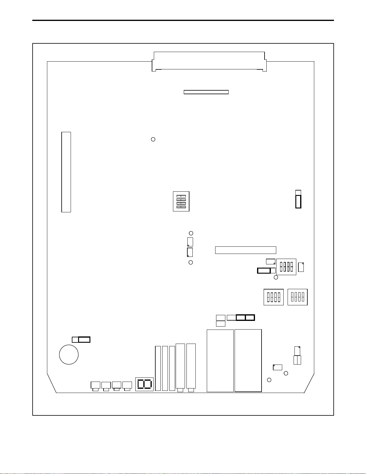
DISPATCH INTERFACE MODULE (DIM)
P1
J31
11 10 9 8 7 6 5 4 3 2 1
TP5
33 1
64 32
1
P2
4
3
2
S5
1
ON
8
J36
132
7
6
5
4
3
2
TP4
R86
987654321
11
10
R83
J32
R80
2
TP3
J27
1
3
432
R77
ON
1
S1
TP6
J24
S2
21
J15
R90
S4
ON
123
21
J14
J21
J22
S3
654
2
1
2
1
2
3
1
P33
ON
4
123
4
132
(LINE)
J2
MAIN OUTPUT (Tx)
R102
TP8
CR401
CR403
J1
J12
J13
CR402
DS1
CR404
J11
R44
R41
MAIN INPUT (Rx)
TP9
MON/
LINE
EQU
(YEL)
(GRN)
(RED)
(GRN)
EQU
MON/
LINE
Figure 11-1 ALIGNMENT POINTS DIAGRAM
11-5
Page 98

FROM MAIN
BOARD
2175 Hz
BANDPASS FILTER
U216
U203
U217C
2175 Hz
NOTCH FILTER
HIGH LEVEL DETECTOR
U210A/B
U211A
LOW LEVEL DETECTOR
U210C/D
U211B
DISPATCH INTERFACE MODULE (DIM)
U206
TO MAIN BOARD
TO MAIN BOARD
TRANSMIT DTMF
U201B/D
U202
U209
U201A/C
TONE GENERATOR
U212
U218
DTMF ENCODER
U201A/C
U204A/B
U214A/B
Q204/Q205
TONE LEVEL CONTROL
U205
U208
Figure 11-2 PTT TONE REMOTE CARD BLOCK DIAGRAM
DAT A
BUS
11-6
Page 99

TP37
DISPATCH INTERFACE MODULE (DIM)
P1
1
33
123
45678
F3
F2
F1
3
2
1
J33
32
64
TP31
+ C62
64/128
256
128/256
J25
23
1
1
U49
2
468
3
579
J15
10
8
7
TP36
J11
23
1
J32
J13
J14
J12
23
1
123
123
+ C65
TP34
U30
8
7
14
1
R93
TP33
TP35
14
1
U29
8
7
1
2
468
3
579
J16
10
J24
123
14
1
J30
R75
S1
1
2
J26
CR7
CR8
CR6
CR5
(YEL)
(YEL)
(GRN)
(YEL)
CR10
(RED)
CR9
(GRN)
Figure 11-3 PTT TONE REMOTE CARD ALIGNMENT POINTS DIAGRAM
11-7
Page 100

DISPATCH INTERFACE MODULE (DIM)
This page intentionally left blank.
11-8
 Loading...