


™
Trion
T20 BGA256
Development Kit User Guide
T20F256-DK-UG-v1.0
February 2019
www.efinixinc.com
Copyright © 2019. All rights reserved. Efinix, the Efinix logo, Quantum, Trion, and Efinity are trademarks of Efinix, Inc. All other trademarks and service
marks are the property of their respective owners. All specifications subject to change without notice.

Contents
Introduction...................................................................................................................................................................... 3
What's in the Box?....................................................................................................................................................... 3
Software Requirements...............................................................................................................................................3
Installing Standoffs......................................................................................................................................................... 3
Board Functional Description...................................................................................................................................... 4
Features...........................................................................................................................................................................4
Overview......................................................................................................................................................................... 5
Power On........................................................................................................................................................................ 6
Reset.................................................................................................................................................................................6
Clock Sources................................................................................................................................................................ 7
Headers........................................................................................................................................................................... 7
User Outputs................................................................................................................................................................ 13
User Inputs.................................................................................................................................................................... 14
Running the Demonstration Design..........................................................................................................................15
Creating Your Own Design.........................................................................................................................................16
Revision History.............................................................................................................................................................16

Introduction
Thank you for choosing the Trion™ T20 BGA256 Development Kit (part number:
T20F256C-DK), which allows you to explore the features of the T20 FPGA with a MIPI
interface.
Warning: The board can be damaged without proper anti-static handling.
What's in the Box?
The Trion™ T20 BGA256 Development Kit includes:
• Trion™ T20 BGA256 Development Board preloaded with a demonstration design
• 4 standoffs
• 4 screws
• 3 foot micro-USB cable (type B)
Trion T20 BGA256 Development Kit User Guide
Software Requirements
To develop your own designs for the T20 device on the board, you must install the Efinity
software. You can obtain the software from the Efinix® Support Center under Efinity
Software (www.efinixinc.com/support/).
The Efinity® software includes tools to program the device on the board. Refer to the
Efinity® Software User Guide for information about how to program the device.
Learn more: Efinity® documentation is installed with the software (see Help > Documentation) and is also
available in the Support Center under Documentation (www.efinixinc.com/support/).
Installing Standoffs
Before using the board, attach the 4 standoffs to the board with the screws provided in the
kit.
Warning: The board can be damaged if you over tighten the screws. Tighten all screws to a torque between
4 ± 0.5 kgf/cm and 5 ± 0.5 kgf/cm.
®
www.efinixinc.com 3
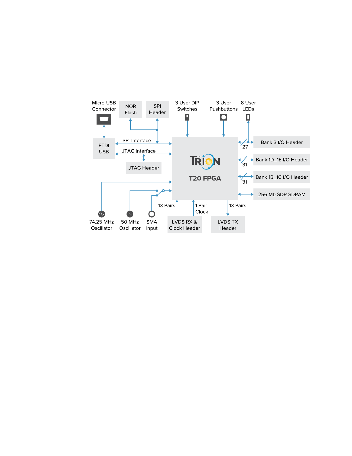
Board Functional Description
The Trion™ T20 BGA256 Development Board contains a variety of components to help you
build designs for the Trion® T20 device.
Figure 1: Trion™ T20 BGA256 Development Board Block Diagram
Trion T20 BGA256 Development Kit User Guide
Features
• Compact design (106.7 mm x 76.2 mm) (4.2" x 3")
• Efinix® T20F256C device in an 256-ball FineLine BGA package
• FTDI FT2232H dual-channel chipset with USB controller
• Winbond 32 Mbit SPI NOR flash memory
• Micro-USB type AB receptacle
• Power:
— Power source: 5 V 4 A power supply or USB 5 V, 500 mA USB (for low-power
consumption designs)
— On-board switching regulators (maximum at 2.0 A) source 3.3 V, 2.5 V, and 1.2 V
components; one on-board dropout regulator (maximum at 500 mA) sources 1.8 V
components
— Selectable 3.3 V, 2.5 V, and 1.8 V VDDIO for T20F256C I/O banks 1D_1E and
1B_1C
— Fixed 3.3 V VDDIO for T20F256C I/O banks 1A, 3, and 4
— 5 V output header to provide power for external devices
• 50 MHz and 74.25 MHz oscillators for T20F256C PLL input
• Optional external clock source available through SMA input to drive the T20F256C PLL
input or clock input pin
www.efinixinc.com 4
• User inputs:
256 Mb SDR SDRAM
Micro-USB
Port (CON2)
50 MHz Oscillator
GPIO Banks
1B, 1C (H4)
Clock Select Header (J3)
(On-Board Oscillator or SMA)
5 V DC Input
Jack (CON1)
GPIO Bank 3 (H3)
FTDI Module
SMA Clock Input (J5)
LVDS Receiver (RX)
& Clock (CON3)
LVDS Transmitter (TX)
(CON4)
5 V Power for
External Devices
GPIO Banks
1D, 1E (H2)
Power Switch (S2)
SPI Header (H1)
JTAG Header (H6)
CDONE (D1) &
User DIPswitches (SW3)
User Pushbuttons (SW4 - SW6)
User LEDs (D3 - D10)
Banks 1B/1C
Voltage Select (H7)
Banks 1D/1E
Voltage Select (H8)
Trion FPGA
T20BGA256C
— 8 LEDs on T20F256C bank 3 for user outputs
— 3 pushbutton switches (connected to bank 1A I/O pins)
— 3 DIPswitches (connected to bank 3 I/O pins) for user inputs
• 3 GPIO headers and 2 LVDS headers to connect to external devices
• Power good and T20F256C configuration done LEDs
Overview
The board features the Efinix® T20 programmable device in a 256-ball FBGA package, which
is fabricated using Efinix® Quantum™ technology. The Quantum™-accelerated programmable
logic and routing fabric is wrapped with an I/O interface in a small footprint package. T20
devices also include embedded memory blocks and multiplier blocks (or DSP blocks). You
create designs for the T20 device in the Efinity® software, and then download the resulting
configuration bitstream to the board using the USB connection.
Note: For more information on T20 FPGAs, refer to the T20 Data Sheet, which you can download in our
Support Center under Docs (www.efinixinc.com/support/).
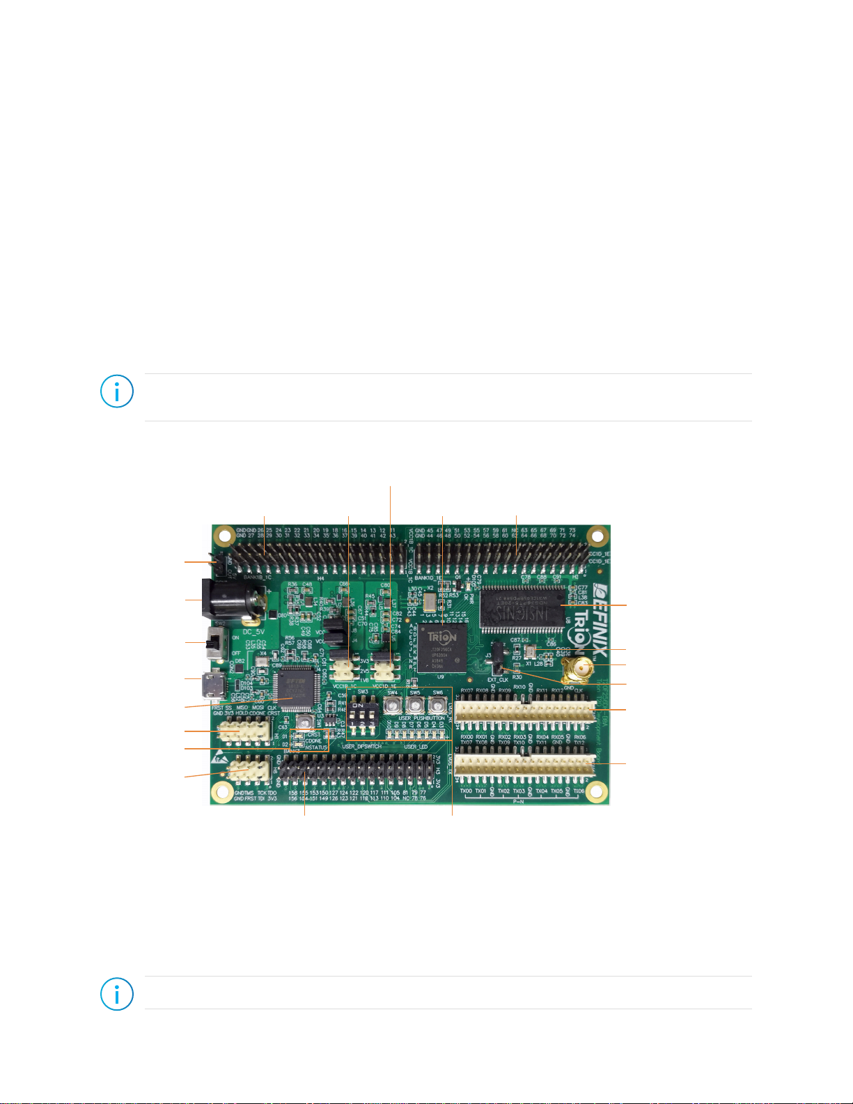
Figure 2: Trion™ T20 BGA256 Development Board Components
Trion T20 BGA256 Development Kit User Guide
The FTDI FT2232H module has two channels to support SPI (FTDI interface 0) and
JTAG (FTDI interface 1) configuration. It receives the T20 configuration bitstream from a
USB host and writes to the on-board SPI NOR flash memory. After a reset in SPI passive
mode, the FTDI controller can also write the configuration bitstream directly to the
FPGA. Additionally, it supports direct JTAG programming mode in which it writes the
configuration bitstream directly to the FPGA through the JTAG interface.
Note: Refer to AN 006 Configuring Trion FPGAs for more information.
www.efinixinc.com 5

Trion T20 BGA256 Development Kit User Guide
The SPI NOR flash memory stores the configuration bitstream it receives from the FTDI
FT2232H module. The T20 device accesses this configuration bitstream when it is in active
configuration mode (default).
The SDRAM device provides 256 Mb of memory and has a 16-bit data bus with 4 banks.
The board's main power supply is the 5V DC input. You must use your own DC power
supply to provide the board with power through the 5 V input jack. The recommended
power input is a 5 V (4 A maximum) DC power source. You can also power the board
through the micro USB port for designs with low power consumption (< 500 mA).
The board regulates down the 5 V DC input using on-board switching regulators to provide
the necessary voltages for the T20 device, SPI flash memory, SDRAM and on-board
oscillator.
Power On
To turn on the development board, turn on switch SW2. Upon power-up, the 5 V DC power
supply or micro-USB power is input to the on-board regulators through 5 V input jack
(CON1) to generate the required 3.3 V, 2.5 V, 1.8 V, and 1.2 V for components on the board.
When these voltages are up and stable, the board asserts a PWR OK signal (pulled high) from
the components' respective regulators. When the board asserts the PWR OK signal, a green
LED (D105) turns on, giving you a visual confirmation that the power supplies on the board
are up and stable.
Note: The micro-USB power supply powers up the board with limited current supply. Efinix recommends that
you use an external DC 5 V DC supply if your user design requires high power.
Reset
The T20F256C device is typically brought out of reset with the CRESET signal. Upon power
up, the T20F256C device is held in reset until CRESET toggles high-low-high.
Note: You can manually assert the high-low-high transition with pushbutton switch SW1.
CRESET has a pull-up resistor. When you press SW1, the board drives CRESET low; when
you release SW1, the board drives CRESET high. Thus, a single press of SW1 provides the
required high-low-high transition.
After toggling CRESET, the T20F256C device goes into configuration mode and reads the
device configuration bitstream from the flash memory. When configuration completes
successfully, the device drives the CDONE signal high. CDONE is connected to a green LED
(D1), which turns on when the T20F256C device enters user mode.
www.efinixinc.com 6

Trion T20 BGA256 Development Kit User Guide
Clock Sources
Two on-board oscillators, 50 MHz and 74.25 MHz, are available to drive the T20F256C PLL
input pin and clock input. Alternatively, you can disable the 50 MHz oscillator and use an
external clock source through the SMA input (J5). Set jumper J3 to use the 50 MHz or SMA
input as the clock source.
Clock Source PLL Input Pin Clock Input Pin
50 MHz oscillator or SMA input GPIOR_157_PLLIN GPIOR_125_CLK10
74.25 MHz oscillator GPIOL_75_PLLIN1 –
You can supply a clock to the PLL or clock network in the FPGA through a board header.
Refer to H2, H3, and H4 under Headers on page 7 for the dedicated clock pins.
Headers
The board contains a variety of headers to provide power, inputs, and outputs, and to
communicate with external devices or boards.
Table 1: Trion™ T20 BGA256 Development Board Headers
Reference Designator Description
CON1 5 V DC power supply input jack
CON2 Micro-USB Type-AB receptacle
CON3 34-pin header for LVDS receiver (RX) and LVDS receiver clock (CLK)
CON4 34-pin header for LVDS transmitter (TX)
H1 SPI header
H2 36-pin header for bank 1D and 1E I/O
H3 36-pin header for bank 3 I/O
H4 36-pin header for bank 1B and 1C I/O
H6 JTAG header
H7 Selects 3.3 V, 2.5 V, or 1.8 V power for banks 1B and 1C
H8 Selects 3.3 V, 2.5 V, or 1.8 V power for banks 1D and 1E
J1 2-pin header for 5 V output
J3 3-pin header to select whether to use the on-board 50 MHz oscillator or SMA input
from external clock source
J5 SMA connector for external 3.3 V clock source input
Header CON1 (5 V Power)
CON1 is a 5 V DC power supply input jack. CON1 supplies power to regulators on the
board that power the T20F256C FPGA. The maximum current supply to this input jack is
4 A.
www.efinixinc.com 7

Trion T20 BGA256 Development Kit User Guide
LVDS RX
Clock Pin
For the differential pair:
Left pin is the P channel
Right pin is the N channel
RX Channel
TX Channel
Header CON2 (USB Power)
CON2, a micro-USB type B socket, is the interface between the board and your computer for
power and communication. Connect the micro-USB cable for configuring T20F256C FPGA
and NOR flash. The board supports three different configuration modes: SPI passive mode,
SPI active mode, and JTAG mode. The USB cable provides a maximum of 500 mA.
Headers CON3 and CON4 (LVDS)
CON3 and CON4 contain the LVDS signals. CON3 has 13 dedicated LVDS RX channels,
and one dedicated LVDS RX clock. CON4 has 13 dedicated LVDS TX channels. You can use
LVDS pins for use as GPIO.
Learn more: Refer to the Trion Interfaces User Guide for instructions on use the LVDS pins as GPIO.
Figure 3: LVDS Headers CON3 and CON4
Table 2: CON3 Pin Assignments
Pin
Number
1 GPIOB_CLKN0 2 GPIOB_RXN06
3 GPIOB_CLKP0
5 GND Ground 6 GND Ground
7 GPIOB_RXN12 8 GPIOB_RXN05
9 GPIOB_RXP12
11 GPIOB_RXN11 12 GPIOB_RXN04
13 GPIOB_RXP11
15 GND Ground 16 GND Ground
17 GPIOB_RXN10 18 GPIOB_RXN03
19 GPIOB_RXP10
21 GPIOB_RXN09 22 GPIOB_RXN02
23 GPIOB_RXP09
25 GND Ground 26 GND Ground
T20F256C
Pin Name
Description Pin
Dedicated LVDS RX
clock
Dedicated LVDS RX
Channel 12
Dedicated LVDS RX
Channel 11
Dedicated LVDS RX
Channel 10
Dedicated LVDS RX
Channel 9
Number
4 GPIOB_RXP06
10 GPIOB_RXP05
14 GPIOB_RXP04
20 GPIOB_RXP03
24 GPIOB_RXP02
T20F256C
Pin Name
Description
Dedicated LVDS RX
Channel 6
Dedicated LVDS RX
Channel 5
Dedicated LVDS RX
Channel 4
Dedicated LVDS RX
Channel 3
Dedicated LVDS RX
Channel 2
www.efinixinc.com 8

Trion T20 BGA256 Development Kit User Guide
Pin
Number
27 GPIOB_RXN08 28 GPIOB_RXN01
29 GPIOB_RXP08
31 GPIOB_RXN07 32 GPIOB_RXN00
33 GPIOB_RXP07
T20F256C
Pin Name
Description Pin
Dedicated LVDS RX
Channel 8
Dedicated LVDS RX
Channel 7
T20F256C
Number
30 GPIOB_RXP01
34 GPIOB_RXP00
Pin Name
Table 3: CON4 Pin Assignments
Pin
Number
1 GPIOB_TXN12 2 GPIOB_TXN06
3 GPIOB_TXP12
5 GND 6 GND Ground
7 GND 8 GPIOB_TXN05
9 GND
11 GPIOB_TXN11 12 GPIOB_TXN04
13 GPIOB_TXP11
15 GND Ground 16 GND Ground
T20F256C
Pin Name
Description Pin
Dedicated LVDS TX
Channel 12
Ground
Dedicated LVDS TX
Channel 10
T20F256C
Number
4 GPIOB_TXP06
10 GPIOB_TXP05
14 GPIOB_TXP04
Pin Name
Description
Dedicated LVDS RX
Channel 1
Dedicated LVDS RX
Channel 0
Description
Dedicated LVDS TX
Channel 6
Dedicated LVDS TX
Channel 5
Dedicated LVDS TX
Channel 4
17 GPIOB_TXN10 18 GPIOB_TXN03
19 GPIOB_TXP10
21 GPIOB_TXN09 22 GPIOB_TXN02
23 GPIOB_TXP09
25 GND Ground 26 GND Ground
27 GPIOB_TXN08 28 GPIOB_TXN01
29 GPIOB_TXP08
31 GPIOB_TXN07 32 GPIOB_TXN00
33 GPIOB_TXP07
Dedicated LVDS TX
Channel 9
Dedicated LVDS TX
Channel 8
Dedicated LVDS TX
Channel 7
Dedicated LVDS TX
Channel 6
20 GPIOB_TXP03
24 GPIOB_TXP02
30 GPIOB_TXP01
34 GPIOB_TXP00
Dedicated LVDS TX
Channel 3
Dedicated LVDS TX
Channel 2
Dedicated LVDS TX
Channel 1
Dedicated LVDS TX
Channel 0
Header H1 (SPI)
H1 is a SPI interface that you can use to configure the on-board NOR flash or T20F256C
FPGA.
Table 4: H1 Pin Assignment
Pin Number Signal Name Description T20F256C Pin Name
1 CRESET_B Configuration reset pin (active low) CRESET_N
2 SPI_CLK SPI configuration clock GPIOL_01_CCK
3 CDONE Configuration done status pin CONDONE
4 SPI_MOSI SPI serial data output GPIOL_08_CDI0
5 HOLD SPI hold pin (active low) –
6 SPI_MISO SPI serial data input GPIOL_09_CDI1
7 3V3 3.3 V power supply –
www.efinixinc.com 9

Trion T20 BGA256 Development Kit User Guide
Pin Number Signal Name Description T20F256C Pin Name
8 SPI_SS SPI slave select pin (active low) GPIOL_00_SS
9 GND Ground –
10 FT_RST Reset pin for on board FTDI FT2232
chipset (active low)
Headers H2, H3, and H4 (GPIO)
The board headers H2, H3, and H4 contain the Trion T20 Development Board GPIO pins.
• H2 (36 pins) links to bank 1D and 1E GPIO pins. You select the VCCIO with the pins on
header H8. Refer to Headers H7 and H8 on page 12 for details.
• H3 (32 pins) links to bank 3 GPIO pins. VCCIO is fixed at 3.3 V.
• H4 (36 pins) links to bank 1B and 1C GPIO pins. You select the VCCIO with the pins on
header H7. Refer to Headers H7 and H8 on page 12 for details.
Table 5: H2 Pin Assignments
Pin Number T20F256C
Pin Name
1 VCCIO1D_1E – 2 VCCIO1D_1E –
3
GPIOL_74
(1)
5 GPIOL_72 No 6 GPIOL_71 No
7
GPIOL_70
(2)
9 GPIOL_68 No 10 GPIOL_67 No
11 GPIOL_66 No 12 GPIOL_65 No
DDIO Mode
Pin Number T20F256C
Supported
No 4 GPIOL_73 No
No 8
Pin Name
GPIOL_69
–
DDIO Mode
Supported
(2)
No
13 GPIOL_64 No 14 GPIOL_63 No
15 GPIOL_62 No 16 – –
17 GPIOL_60 Yes 18 GPIOL_61 Yes
19 GPIOL_58 Yes 20 GPIOL_59 Yes
21 GPIOL_56 Yes 22 GPIOL_57 Yes
23 GPIOL_54 Yes 24 GPIOL_55 Yes
25 GPIOL_52 Yes 26 GPIOL_53 Yes
27 GPIOL_50 Yes 28 GPIOL_51 Yes
29 GPIOL_48 Yes 30 GPIOL_49 Yes
31 GPIOL_46 Yes 32 GPIOL_47 Yes
33 GPIOL_44 Yes 34 GPIOL_45 Yes
35 GND – 36 GND –
(1)
Dedicated PLL input pin that supplies the clock to FPGA's PLL.
(2)
If you are using multi-image configuration, GPIOL_69 and GPIOL_70 are the CBSEL[1] and CBSEL[0] pins that select the image
to use. For more information, refer to AN 006: Configuring Trion FPGAs
www.efinixinc.com 10

Table 6: H3 Pin Assignments
Trion T20 BGA256 Development Kit User Guide
Pin Number T20F256C
Pin Name
DDIO Mode
Supported
Pin Number T20F256C
Pin Name
1 3V3 – 2 3V3 –
3
GPIOR_76
(1)
No 4
GPIOR_77
(1)
7 GPIOR_78 No 8 GPIOR_79 No
9 – – 10 GPIOR_81 No
5 GPIOR_104 Yes 6 GPIOR_105 Yes
11 GPIOR_110 Yes 12 GPIOR_111 Yes
13 GPIOR_113 Yes 14 GPIOR_117 Yes
15 GPIOR_118 Yes 16
17
19
21
GPIOR_121
GPIOR_123
GPIOR_126
(3)
(3)
(3)
Yes 18
Yes 20
Yes 22
GPIOR_120
GPIOR_122
GPIOR_124
GPIOR_127
(3)
(3)
(3)
(3)
23 GPIOR_149 Yes 24 GPIOR_150 Yes
25 GPIOR_151 Yes 26 GPIOR_153 Yes
27 GPIOR_154 Yes 28 GPIOR_155 Yes
29 GPIOR_156 Yes 30 GPIOR_158 Yes
DDIO Mode
Supported
No
Yes
Yes
Yes
Yes
31 GND – 32 GND –
Table 7: H4 Pin Assignments
Pin Number T20F256C
Pin Name
1 VCCIO1B_1C – 2 VCCIO1B_1C –
3 GPIOL_43 Yes 4 GPIOL_11 Yes
5 GPIOL_42 Yes 6 GPIOL_12 Yes
7 GPIOL_41 Yes 8 GPIOL_13 Yes
9 GPIOL_40 Yes 10 GPIOL_14 Yes
11 GPIOL_39 Yes 12 GPIOL_15 Yes
13 GPIOL_37 Yes 14 GPIOL_16 Yes
15 GPIOL_36 Yes 16 GPIOL_18 Yes
17 GPIOL_35 Yes 18 GPIOL_19 Yes
19 GPIOL_34 Yes 20 GPIOL_20 Yes
21 GPIOL_33 Yes 22 GPIOL_21 Yes
23 GPIOL_32 Yes 24 GPIOL_22 Yes
25
27
GPIOL_31
GPIOL_30
DDIO Mode
Supported
(3)
(3)
Yes 26 GPIOL_23 Yes
Yes 28
Pin Number T20F256C
Pin Name
GPIOL_24
DDIO Mode
Supported
(3)
Yes
(3)
Dedicated clock input pin that supplies the clock to global clock network.
www.efinixinc.com 11

Trion T20 BGA256 Development Kit User Guide
Pin Number T20F256C
Pin Name
29
31
33
GPIOL_29
GPIOL_28
GPIOL_27
(3)
(3)
(3)
DDIO Mode
Supported
Yes 30
Yes 32
Pin Number T20F256C
Pin Name
GPIOL_25
GPIOL_26
(3)
(3)
Yes 34 GND –
35 GND – 36 GND –
Header H6
Header H6 is the JTAG interface. You can access the T20F256C JTAG pins through this
header.
Pin Number Signal Name Description
1 3V3 3.3 V power supply
2 TDO JTAG data output signal
3 TDI JTAG data input signal
4 TCK JTAG clock signal
5 FT_RST Reset pin for on board FTDI FT2232 module
(active low)
6 TMS JTAG TMS mode select signal
DDIO Mode
Supported
Yes
Yes
7 GND Ground
8 GND Ground
Headers H7 and H8
H7 and H8 are 6-pin headers. You use a shunt across 2 pins to select 3.3 V, 2.5 V, or 1.8 V
for the T20F256C bank VCCIO1B_1C and VCCIO1D_1E, respectively, from the on-board
regulators.
By default, the board ships with a shunt connecting pins 5 and 6 to supply 3.3 V.
Table 8: Voltage Selection for VCCIO1B_1C and VCCIO1D_1E
Shunt VCCIO1B_1C (H7) VCCIO1D_1E (H8)
Connect pins 1 and 2 1.8 V 1.8 V
Connect pins 3 and 4 2.5 V 2.5 V
Connect pins 5 and 6 3.3 V (default) 3.3 V (default)
Caution: Only select one voltage at a time. Installing more than one shunt on H7 or H8 may cause contention.
www.efinixinc.com 12

Trion T20 BGA256 Development Kit User Guide
Header J1
J1 is a 2-pin header that provides 5 V output as a power source for the external devices that
interface with the development board. The 5 V DC power supply from header CON1
supplies this 5 V output.
Table 9: J1 Pin Assignments
Pin Number Signal
1 5V
2 GND
Note: If you are supplying power to the board using the micro-USB cable only, limited power is available
(<500 mA).
Headers J3 and J5
J3 is a 3-pin header used to select the source for the T20F256C clock input and PLL input.
Drive a 3.3 V clock source input into the SMA connector, J5, if you are using the external
clock source option.
Table 10: Clock Selection Pin Assignments
Pin Number Signal
1 50 MHz on-board oscillator
2 GPIOR_125_CLK10 and GPIOR_157_PLLN
3 External clock source from SMA input J5
• A shunt connecting J3 pins 1 and 2 selects the 50 MHz on-board oscillator (default).
• A shunt connecting J3 pins 2 and 3 selects the clock source from SMA input J5.
User Outputs
The board has 8 green user LEDs that are connected to I/O pins in T20F256C banks 1A/1B.
By default, the T20F256C I/O connected to these LEDs have a pull-up resistor that turns the
LEDs off; to turn a given LED on, pull the corresponding I/O signal low.
Table 11: User Outputs
Reference Designator T20F256C Pin Name Active
D3 GPIOR_104 Low
D4 GPIOR_105 Low
D5 GPIOR_117 Low
D6 GPIOR_118 Low
D7 GPIOR_153 Low
D8 GPIOR_154 Low
D9 GPIOR_155 Low
D10 GPIOR_156 Low
www.efinixinc.com 13

Trion T20 BGA256 Development Kit User Guide
User Inputs
The board has 3 pushbutton switches that you can use as inputs to the T20F256C device. The
T20F256C bank 1A I/O signals connected to these switches have a pull-up resistor. When
you press the switch, the signal drives low, indicating user input.
User Pushbuttons
Table 12: User Pushbuttons
Reference Designator T20F256C Pin Name Active
SW4 GPIOL_02 Low
SW5 GPIOL_04 Low
SW6 GPIOL_05 Low
User DIPswitches
Table 13: User DIPswitches
Reference Designator T20F256C Pin Name Off (Default) On
SW3.1 GPIOL_128 Low High
SW3.2 GPIOL_129 Low High
SW3.3 GPIOL_130 Low High
www.efinixinc.com 14

Running the Demonstration Design
Connect a power
cable to the board
and your computer
CDONE LED (D1)
NSTATUS LED (D2)
Turn on the
power switch
1
2
PWR OK LED D105
Press and hold
pushbutton SW4
3
Press and hold
pushbutton SW5
4
Press and hold
pushbutton SW6
5
LEDs (D3 - D10)
Efinix® preloads the Trion™ T20 BGA256 Development Board with a demonstration design
that operates the LEDs. The board receives power through USB cable. Follow these steps to
run the design:
1. Connect the 5 V DC power source or USB cable to the board and to your computer.
2. Turn on the power switch (SW2). LED D105 (PWR OK) turns on, indicating that the
board is receiving power correctly.
Note: The Trion™ T20 BGA256 Development Kit does not include a DC power
adapter.
• While configuration is in process, the configuration done LED D1 (CDONE) turns
OFF to indicate the device is in configuration mode.
• At the same time, the LED D2 (NSTATUS) turns ON to indicate there is no
configuration error.
• When configuration completes, the configuration done LED (D1) turns on again. Four
green LEDs (D3 - D10) turn on, sweeping from D3 to D10 in ascending order.
Trion T20 BGA256 Development Kit User Guide
Note: If LED D105 does not turn off, the board is not receiving power correctly.
3. Press and hold pushbutton SW4. The LEDs blink alternately between group 1 (D3, D5,
D7, and D9) and group 2 (D4, D6, D8, and D10).
4. Press and hold pushbutton SW5. The LEDs all blink on and off alternatively.
5. Press and hold pushbutton SW6. The LEDs sweep in backwards order from D10 to D3
Figure 4: Running the Demonstration Design
www.efinixinc.com 15

Creating Your Own Design
The Trion™ T20 BGA256 Development Board allows you to create and explore designs for
the T20 device. Efinix® provides example code and designs to help you get started:
• Refer to the Design Support page in our Support Center (www.efinixinc.com/support)
for examples targeting the board.
• The Efinity software includes example designs that you can use as a starting point for your
own project.
Note: For more information, email support@efinixinc.com.
Revision History
Table 14: Revision History
Trion T20 BGA256 Development Kit User Guide
Date Version Description
February 2019 1.0 Initial release.
www.efinixinc.com 16
 Loading...