

Page 1
User’s Guide
HRC
Mezzanine Board
High Rate Carrier (E4, STS3, OC3 / STM1)
for use with a PCI / PCIe Main Board
Doc. 008-02006-03a
Rev. 2013 January 22
Contact
Sky Blue Microsystems GmbH
Geisenhausenerstr. 18
81379 Munich, Germany
+49 89 780 2970, info@skyblue.de
www.skyblue.de
In Great Britain:
Zerif Technologies Ltd.
H5 Ash Tree Court
Nottingham NG8 6PY, England
+44 115 855 7883, info@zerif.co.uk
www.zerif.co.uk
Page 2

TM
EDT
and Engineering Design TeamTM are trademarks of Engineering Design Team, Inc. All other trademarks, service marks,
and copyrights are the property of their respective owners†.
© 1997-2013 Engineering Design Team, Inc. All rights reserved.
Contact
Sky Blue Microsystems GmbH
Geisenhausenerstr. 18
81379 Munich, Germany
+49 89 780 2970, info@skyblue.de
www.skyblue.de
EDT, Inc. 2
In Great Britain:
Zerif Technologies Ltd.
H5 Ash Tree Court
Nottingham NG8 6PY, England
+44 115 855 7883, info@zerif.co.uk
www.zerif.co.uk
Page 3

Terms of Use Agreement
Definitions. This agreement, between Engineering Design Team, Inc. (“Seller”) and the user or distributor (“Buyer”), covers the
use and distribution of the following items provided by Seller: a) the binary and all provided source code fo r any and all device
drivers, software libraries, utilities, and example applications (collectively, “Software”); b) the binary and all provided source code
for any and all configurable or programmable devices (collectively, “Firmware”); and c) the computer boards and all other physical
components (collectively, “Hardware”). Software, Firmware, and Hardware are collectively referred to as “Products.” This
agreement also covers Seller’s published Limited Warranty (“Warranty”) and all other published manuals and product information
in physical, electronic, or any other form (“Documentation”).
License. Seller grants Buyer the right to use or distribute Seller’s Software and Firmware Products solely to enable Seller’s
Hardware Products. Seller’s Software and Firmware must be used on the same computer as Seller’s Hardware. Seller’s Products
and Documentation are furnished under, and may be used only in accordance with, the terms of this agreement. By using or
distributing Seller’s Products and Documentation, Buyer agrees to the terms of this agreement, as well as any additional
agreements (such as a nondisclosure agreement) between Buyer and Seller.
Export Restrictions. Buyer will not permit Seller’s Software, Firmware, or Hardware to be sent to, or used in, any other country
except in compliance with applicable U.S. laws and regulations. For clarification or advice on such laws and regulations, Buyer
should contact: U.S. Department of Commerce, Export Division, Washington, D.C., U.S.A.
Limitation of Rights. Seller grants Buyer a royalty-free right to modify, reproduce, and distribute executable files using the
Seller’s Software and Firmware, provided that: a) the source code and executable files will be used only with Seller’s Hardware;
b) Buyer agrees to indemnify, hold harmless, and defend Seller from and against any claims or lawsuits, including attorneys’ fees,
that arise or result from the use or distribution of Buyer’s products containing Seller’s Products. Seller’s Hardware may not be
copied or recreated in any form or by any means without Seller’s express written consent.
No Liability for Consequential Damages. In no event will Seller, its directors, officers, employees, or agents be liable to Buyer
for any consequential, incidental, or indirect damages (including damages for business interruptions, loss of business profits or
information, and the like) arising out of the use or inability to use the Products, even if Seller has been advised of the possibility
of such damages. Because some jurisdictions do not allow the exclusion or limitation of liability for consequential or incidental
damages, the above limitations may not apply to Buyer. Seller’s liability to Buyer for actual damages for any cause whatsoever,
and regardless of the form of the action (whether in contract, product liability, tort including negligence, or otherwise) will be
limited to fifty U.S. dollars ($50.00).
Limited Hardware Warranty. Seller warrants that the Hardware it manufactures and sells shall be free of defects in materials
and workmanship for a period of 12 months from date of shipment to initial Buyer. This warranty does not apply to any product
that is misused, abused, repaired, or otherwise modified by Buyer or others. Seller’s sole obligation for breach of this warranty
shall be to repair or replace (F.O.B. Seller’s plant, Beaverton, Oregon, USA) any goods that are found to be non-conforming or
defective as specified by Buyer within 30 days of discovery of any defect. Buyer shall bear all installation and transportation
expenses, and all other incidental expenses and damages.
Limitation of Liability. In no event shall Seller be liable for any type of special consequential, incidental, or penal damages,
whether such damages arise from, or are a result of, breach of contract, warranty, tort (including negligence), strict liability, or
otherwise. All references to damages herein shall include, but not be limited to: loss of profit or revenue; loss of use of the goods
or associated equipment; costs of substitute goods, equipment, or facilities; downtime costs; or claims for damages. Seller shall
not be liable for any loss, claim, expense, or damage caused by, contributed to, or arising out of the acts or omissions of Buyer,
whether negligent or otherwise.
No Other Warranties. Seller makes no other warranties, express or implied, including without limitation the implied warranties
of merchantability and fitness for a particular purpose, regard ing Seller’s Products or Documentation. Seller does not warrant,
guarantee, or make any representations regarding the use or the results of the use of the Products or Documentation or their
correctness, accuracy, reliability, currentness, or otherwise. All risk related to the results and performance of the Products and
Documentation is assumed by Buyer. The exclusion of implied warranties is not permitted by some jurisdictions. The above
exclusion may not apply to Buyer.
Disclaimer. Seller’s Products and Documentation, including this document, are subject to change without notice. Documentation
does not represent a commitment from Seller.
EDT, Inc. 3
Page 4

Contents
Overview................................................................................................................................................................... 5
DMA: Four-channel vs. Legacy Sixteen-channel......................................................................................... 5
FPGAs on the PCI / PCIe Main Board......................................................................................................... 5
Companion Products.................................................................................................................................... 6
Related Resources....................................................................................................................................... 6
Installation................................................................................................................................................................. 7
About the Software and Firmware................................................................................................................ 7
The PCD Device Driver................................................................................................................................ 7
FPGA Configuration Files ................................................................. ... ... ... ... .... ........................................... 8
Software Initialization Files........................................................................................................................... 8
Sample Applications and Utilities................................................................................................................. 8
Sample Applications.............................................................................................................................. 9
Utility Files............................................................................................................................................. 9
Basic Testing Files ................................................................................................................................ 9
Building or Rebuilding an Application........................................................................................................... 9
Configuring the HRC............................................................................................................................................... 10
Checking or Updating the PCI / PCIe FPGA Firmware.............................................................................. 10
Loading the UI FPGA Firmware and Configuring the HRC........................................................................ 11
Using Custom FPGA Configuration Files................................................................................................... 11
Configuring the Channels ....................................................................................................................................... 11
Basic Testing .......................................................................................................................................................... 11
Connector Pinout .......... ... ... ... .... ... ....................................... ... ... ... .... ... ... ... .... ... ...................................................... 12
Registers................................................................................................................................................................. 13
Revision Log .......... .... ... ... ... ... .... ...................................... .... ... ... ... .... ... ................................................................... 19
EDT, Inc. 4
Page 5

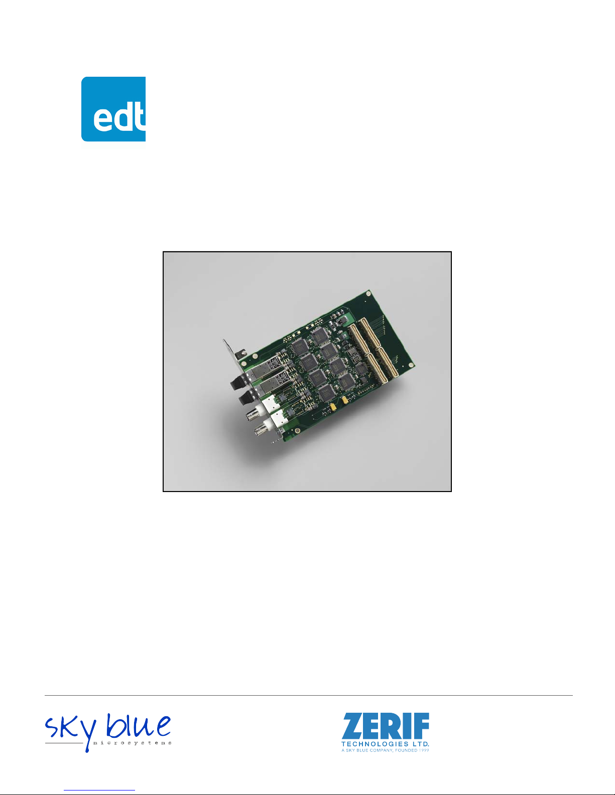
HRC Mezzanine Board
Overview
The HRC Mezzanine Board supports OC3 / STM1, STS3, or E4 signals in various combinations, including
framing and descrambling for OC3 / STM1 framed data. The board allows DMA output at the rate of 139 or
155 Mb/s (DMA is provided through the PCI / PCIe Main Board). The PCI / PCIe interface has bandwidth to
output OC3 / STM1 data on all four HRC channels.
The HRC has four connector locations; each is occupied by either a 75- BNC coaxial interface with CMI-
coded transmission, or a fiber-optic LC with a single-mode 1300 nm transceiver.
The standard connector combinations are: 4 BNC; 4 fiber-optic; 2 of each; or 3 BNC + 1 fiber-optic. Each
BNC can be programmed for either input or output; for bidirectional coaxial operation, a maximum of two
channels is available. The fiber-optic HRC has eight potential data streams (four in and four out), so full
duplex operation on all four fiber ports is not possible.
DMA: Four-channel vs. Legacy Sixteen-channel
Due to the constant filling and flushing of the DMA data pipeline in the host computer, some computers
cannot support the PCI bandwidth required for more than two active HRC outputs. With 16-channel DMA,
DMA burst size is smaller, and the PCI bus cannot switch between channels fast enough. With four-chann el
operation, however, DMA occurs in bigger bursts, with less switching — a more efficient mode of operation.
Therefore, we recommend that you configure new systems for four-channel operation.
However, if you choose to use sixteen-channel operation, you can do so by using the UI FPGA configuration
file
sshrcin.bit, the software initialization file hrcin.cfg, and a PCI FPGA configuration file ending in
...16.bit
available DMA channels (four in and four out), assuming that you have written you r own firmware to do so.
The DMA channels correlate to the HRC inputs and outputs as follows:
Channel 0 = input 0 Channel 2 = input 2 Channel 4 = output 0 Channel 6 = output 2
Channel 1 = input 1 Channel 3 = input 3 Channel 5 = output 1 Channel 7 = output 3
(either pciss16.bit or pcigs16.bit). Thus configured, the HRC can use eight of the sixteen
FPGAs on the PCI / PCIe Main Board
The HRC is paired with an EDT PCI / PCIe Main Board, which has the following FPGAs:
•The user interface (UI) FPGA links the HRC to the main board’s PCI or PCIe FPGA.
•The PCI or PCIe FPGA communicates with the host computer over the PCI or PCIe bus and implements
the DMA engine, which transfers data between the board and the host. This FPGA loads automatically,
at powerup, with the correct firmware from the main board’s FPGA configuration flash memory (“flash
memory”).
For details, consult the PCI / PCIe Main Board User’s Guide (see Related Resources below).
EDT, Inc. 2013 January 22 5
Page 6

HRC Overview
Companion Products
For additional resources, the HRC is designed to work with these EDT products:
• Required – a PCI / PCIe Main Board (PCI SS, PCI GS, or PCIe8 LX / FX), for DMA and other resources
• Optional – a Time Distribution Board, for precise timestamping of the data.
For details on these products, see Related Resources.
Related Resources
The resources below may be helpful or necessary for your applications.
EDT Resources
Description Detail Web link
• HRC specifications Datasheet (on product page) www.edt.com
• PCI / PCIe Main Board information Datasheet and user’s guide www.edt.com/main_boards.html
• Time Distribution board information Datasheet and user’s guide www.edt.com/timedist.html
• Application Programming Interface HTML and PDF versions www.edt.com/manuals.html
• Installation packages:
Windows, Linux, Solaris, Mac
Software / firmware
downloads
www.edt.com/software.html
EDT, Inc. 2013 January 22 6
Page 7

HRC Installation
Installation
To install the HRC, fit the connectors through the host back panel and then plug into the PCI connector. The
BNC is farther from the PCI bus connector, so it can interfere with the host back panel and prevent the
bottom of the HRC back panel from being inserted smoothly. To manipulate the board into position:
1. Place the edge connector between two PCI co nn ec to rs on the mo the r bo ar d.
2. Position the HRC back panel.
3. Lift the board slightly to insert the edge connector into the host socket.
The connector furthest from the PCI / PCIe bus connector is channel 0; see Figure 1 or Figure 2 for details.
About the Software and Firmware
Your EDT installation package includes these HRC-specific files:
sshrc.bit Four-channel version (signals can be either inputs or outputs). Configures the UI
FPGA on the main board to communicate with the HRC for four-channel operation.
sshrcin.bit Legacy sixteen-channel version (signals are inputs only). Configu res the UI FPGA
on the main board to communicate with the HRC for sixteen-channel operation.
The
pcd_config subdirectory contains sample software initialization files for all board configurations.
These files include:
hrc.cfg Four-channel version. Configuration file for initpcd to use to configure the HRC
for four-channel operation.
hrcin.cfg Legacy sixteen-channel version. Configuration file for initpcd to use to configure
the HRC for sixteen-channel operation.
NOTE Additional files are required for the PCI / PCIe Main Board that goes with the HRC mezzanine board.
For details on those files, including how to load and use them, see Related Resources on page 6.
The firmware file names you see in the top-level PCD directory do not match the file names given above
because PCI bus slots come in two varieties: those supplying 3 V power, and those supplying 5 V power.
Different firmware is required for the two kinds of slots, but the correct firmware file is chosen automatically
when you run
For example, you may see files named
supply to load the firmware is
In some cases, you may also see additional firmware files incorporating ch anges required for various board
revisions, or files with the same name in different subdirectories. You need not be concerned with any of
these variations of name or path, however. In all cases, the names given above are the correct arguments
to supply to the firmware-loading utilities.
pciload or any other EDT-supplied firmware loading utility.
cda16_3v.bit and cda16_5v.bit, but the correct argument to
cda16.bit.
The PCD Device Driver
The PCD device driver is the software running on the host that allows the host operating system to
communicate with the HRC. The driver is loaded into the kernel upon installation, and thereafter runs as a
kernel module. The driver name and subdirectory is specific to each supported operating system; the
installation script handles those details for you, automatically installing the correct device driver in the
correct operating system-specific manner.
EDT, Inc. 2013 January 22 7
Page 8

HRC Installation
FPGA Configuration Files
FPGA configuration files define the firmware required for the PCI FPGA and the UI FPGA. The PCI FPGA
firmware files are in the
the
bitfiles subdirectory of the top-level PCD directory.
flash subdirectory of the top-level PCD directory. UI FPGA firmware files are in
Each FPGA must be loaded with the firmware specific to the chosen interface, and the firmware in one
FPGA must be compatible with the firmware in the other. By default, the co rrect FPGA configuration file for
the PCI FPGA is loaded at the factory. However, you’ll need to load the required FPGA configuration file for
the UI FPGA yourself.
The firmware files specific to your HRC are listed at the beginning of this section. Instructions for loading
them are provided in Configuring the HRC.
Software Initialization Files
Software initialization files (.cfg) are editable text files that run like scripts to configure EDT boards so that
they are ready to perform DMA. The commands in a software initialization file are defined in a C application
named
-f
A typical software initialization file loads an FPGA configuration file into the UI FPGA and sets up various
registers to prepare the board for DMA transfers. Some software initialization files may also load an FPGA
configuration file into an FPGA residing on the mezzanine board.
initpcd. When you invoke initpcd, you specify which software initialization file to use with the
flag.
A variety of software initialization files are included with the EDT software, at least one of which is
customized for each main board or main board / mezzanine board combination — that is, each FPGA
configuration file has a matching software initialization file. Software initialization files are located in the
pcd_config subdirectory of the top-level PCD directory. The software initialization files specific to your
HRC are listed at the beginning of this section. Instructions for their use are provided in Configuring the
HRC.
Commands defined in
configuration files to be loaded (for example,
registers (for example,
initpcd and typically found in software initialization files allow for specific FPGA
bitfile:), write specified hexadecimal values to sp ecified
command_reg:), enable or disable byte-swapping or short-swapping to
accommodate different operating systems’ requirements for bit ordering (for example,
invoke arbitrary commands (for example,
bitfile: ssd16io.bit
command_reg: 0x08
byteswap: 1
run_command: set_ss_vco -F 1000000 2
run_command:). For example:
For complete usage details, enter initpcd --help.
C source for
initpcd is included so that you can add your own commands, if you wish. You can then edit
your own software initialization file to use your new commands and specify that
when configuring your board. If you would like us to include your new software initialization commands in
subsequent releases of
initpcd, email us at tech@edt.com.
Sample Applications and Utilities
byteswap:), or
initpcd use your new file
Along with the driver, the FPGA configuration files, and the software initialization files, the EDT installation
CD includes a number of applications and utilities that you can use to initialize and configure the board,
access registers, or test the board. For many of these applications and utiilities, C source is also provided,
EDT, Inc. 2013 January 22 8
Page 9

HRC Installation
so that you can use them as starting points to write your own applications. The most commonly useful are
described below; see the README file for the complete list.
NOTE To build a new application, we recommend downloadin g th e late st EDT installa tio n pa ck ag e (se e
Related Resources). To rebuild an existing application, avoid version issues by using the same package
used to build it, or relink / recompile the application using our latest download package.
Sample Applications
rd16 Performs simple multichannel ring buffer input.
wr16 Performs simple multichannel ring buffer output.
simple_read Performs DMA input without using ring buffers. Data is therefore subject to
interruptions, depending on system performance.
simple_write Performs DMA output without using ring buffers. Data is therefore subject to
interruptions, depending on system performance.
simple_getdata An example of a variety of DMA-related operations, including reading the data from
the connector interface and writing it to a file, as well as measuring input rate.
simple_putdata An example of a variety of DMA-related operations, including read ing data fr om a
file and writing it out to the connector interface.
test_timeout Under normal operation, timeouts cancel DMA transfers. This application
exemplifies giving notification when a timeout occurs, without canceling DMA
set_ss_vco A utility for programming the output clock or clocks on the HRC to specific
frequencies used by the UI FPGA for input and output.
Utility Files
initpcd A utility for initializing and configuring the HRC.
pdb A utility that enables interactive reading and writing of the UI FPGA registers.
Basic Testing Files
EDT provides files to perform basic tests, such as verifying proper installation, on your EDT board (for
details, see Basic Testing). These files include at least:
sslooptest Tests most EDT boards. Determines the board model and runs the correct
loopback test.
Building or Rebuilding an Application
Executable and PCD source files are in the top-level EDT PCD directory. To build or rebuild an application,
therefore, run
make in this directory.
Windows users must install a C compiler, while Linux users can use the
with your Linux installation. If you use Windows, we recommend the Microsoft Visual C compiler; however,
if you wish to use
After you’ve built an application, use the --help command line option for a list of usage options and
descriptions.
EDT, Inc. 2013 January 22 9
gcc, contact tech@edt.com.
gcc compiler typically included
Page 10

HRC Configuring the HRC
Configuring the HRC
To ensure proper functioning, all EDT boards must be loaded with the correct FPGA configuration files for
their FPGAs. At powerup, the PCI / PCIe FPGA is loaded automatically with the correct file from flash
memory; however, you must load the UI FPGA yourself. Before doing so, you may wish to check the
firmware in the PCI / PCIe FPGA to ensure that it is correct and up to date.
Checking or Updating the PCI / PCIe FPGA Firmware
When upgrading to a new device driver, or switching to a FPGA configuration file with special functionality,
you may need to reprogram the PCI / PCIe interface flash memory using
NOTE The presence of a newer version of the firmware with a new driver does not necessarily mean that the
firmware must be updated; the README file will tell you if a package contains a mandatory upgrade.
The following procedure applies to standard firmware only. If you are running a custom fi rmware file and
need to update it, first get a custom firmware configuation file from EDT.
• On Windows systems, double-click the Pcd Utilities icon to bring up a command shell in the installation
directory
\EDT\Pcd.
pciload.
• On Linux systems,
• On Mac systems, pciload is an application in the installation directory /Applications/EDT/pcd.
To see currently installed and recognized EDT boards and drivers, enter:
pciload
The program will output the date and revision number of the firmware in the flash memory.
To compare the PCI / PCIe FPGA firmware in the package with what is already loaded on the board, enter:
pciload verify
If they match, there’s no need to upgrade the firmware. If they differ, you’ll see error messages. This does
not necessarily indicate a problem; if your application is operating correctly, you may not need to upgrade
the firmware. However, if you do wish to update the standard firmware, enter:
pciload update
1. To upgrade or switch to a custom firmware file, enter:
pciload firmware_filename
...replacing firmware_filename with the name of the PCI / PCIe Main Board FPGA configuration file,
with or without the
NOTE If the host computer holds more than one board, you can specify the correct board to load with the
optional
pciload -u unit_number filename
unit_number argument (by default, 0 for the first or only board in a host), as shown:
pciload is an application in the installation directory /opt/EDTpcd.
.bit file extension.
2. At the prompt, press Enter to confirm the loading operation. (If the file date is older than the date of the
file already in flash memory, you may need to pres s Ente r twice .)
The board reloads the firmware from the flash memory only d uring power-up, so after running
the old firmware remains in the PCI / PCIe FPGA until the system has power-cycled.
NOTE Updating the firmware requires cycling power, not simply rebooting.
EDT, Inc. 2013 January 22 10
pciload,
Page 11

HRC Configuring the Channels
For a list of all pciload options, enter:
pciload --help
Loading the UI FPGA Firmware and Configuring the HRC
The utility initpcd loads the UI FPGA configuration files, programs the register s, sets the clocks (if
necessary), and gets the HRC ready to perform DMA. This utility takes, as an argument, a software
initialization file, and then automatically runs the pertinent commands.
If you use
and other application-specific operations; it will therefore omit HRC-specific operations and be portable to
other EDT boards that peform DMA.
To configure the HRC, enter:
...replacing unit_number with the number of the board (by default, 0), and replacing filename with one
of the initialization files listed in About the Software and Firmware; for example:
NOTE Software initialization files are editable text files. If the files provided do not meet your needs, copy and
initpcd to configure the HRC, your application can concern itself solely with performing DMA
initpcd -u unit_number -f pcd_config/filename.cfg
initpcd -f hrc.cfg
modify the one that’s closest to your required configuration; then run
initpcd with your new file.
Using Custom FPGA Configuration Files
You can substitute your own FPGA configuration file, if necessary. If you wish to develop your own VHDL
design, contact EDT. When you’re done, be sure to create a new software initialization file for your new
firmware file and update the
pcd_config directory to include it.
Configuring the Channels
An alternate way to configure the HRC, without using a software initialization file, is to enter:
bitload -u unit_number sshrc.bit
The bitload program detects and loads the main board’s UI FPGA with sshrc.bit.
Basic Testing
The loopback test determines the board configuration, loads the appropriate bitfile, g enerates test data and
tests the board and its components with no external device connected. Test files are included — see About
the Software and Firmware on page 7 for the complete list.
NOTE The loopback test overwrites the bitfile in the UI FPGA. Before you can use the board again, you’ll need
to reconfigure it after the test has completed.
EDT, Inc. 2013 January 22 11
Page 12

HRC Connector Pinout
Channel 0
Channel 1
Channel 2
Channel 3
Channel 3 transmit
Channel 3 receive
Channel 2 transmit
Channel 2 receive
Channel 1 transmit
Channel 1 receive
Channel 0 transmit
Channel 0 receive
To perform this test:
1. Leave the board pair (main + mezzanine) in the host, but disconnect any external device and its cable.
2. In a command window, enter:
sslooptest -u unit_number
The outcome will vary for each type of board. Errors are redirected to the file sslooptest.err in the
current directory; if no such file exists, the test completed without errors.
Loopback test output for a functional board contains such lines as:
Total errs=0 bufs=4000; Channel errs(NNx) bufs(YYx)
Total errs shows the error count so far; bufs shows the number of buffers in use. The three
characters after
(0–3);
x indicates a channel is not in use. Similarly, a Y after Channel... bufs shows a buffer in use;
x, that the corresponding channel is not in use. An N indicates that DMA is not occurring in a specific
Channel errs show the absence (N) or presence (Y) of a data error in a given channel
channel.
3. After the test, reconfigure the board using
4. Reconnect the board to the external device .
Connector Pinout
The connectors connect to the channels as shown in Figure 1 and Figure 2.
Figure 1. Connector Pinout, BNC
Figure 2. Connector Pinout, Fiber-optic
initpcd (or your own application) to disable loopback.
EDT, Inc. 2013 January 22 12
Page 13

HRC Registers
Registers
The following registers are implemented but not used: 0x01 Data Path; 0x03 Status; 0x04 Status Polarity;
and 0x05–06 Direction Control. In addition, addresses 0x56–57 are reserved for internal use.
NOTE The registers shown are for four-channel operation. For sixteen-channel oper ation, the di fferences are:
0x18 Underflow Not used. 0x25 Send / Receive Relay Address is 0x15.
0x22 Channel Loopback Address is 0x12. 0x26 Parallel Data Size Address is 0x1C.
0x23 Channel Clock Address is 0x13. 0x27 Enable Laser Address is 0x1E.
0x24 Channel Clock Source Address is 0x14.
0x00 Command
Access / Notes: 8-bit read-write / PCD_CMD
Bit Name Description
7–4
3
2–0
[no name]
CMD_EN
[no name]
Not used.
Set to enable the FPGA configuration file.
Clear to reset all channels, flush the FIFOs, and clear all under- and overflow bits.
Not used.
0x02 Function
Access / Notes: 8-bit read-write / PCD_CMD
Bit Name Description
7–1
0
[no name]
FUNCT
Not used.
When set, flush output word by word.
When clear, wait for 16 words before transferring to PCI FPGA.
EDT, Inc. 2013 January 22 13
Page 14

HRC Registers
0x0F Configuration
Access / Notes: 8-bit read-write / PCD_CONFIG
Use this register and 0x16, 17 Least Significant Bit First to control how the data is ordered.
This register implements swapping. The structure of a 32-bit data word without swapping is:
short 1 short 0
31 30 29 28 27 26 25 24 23 22 21 20 19 18 17 16 15 14 13 12 11 10 9 8 7 6 5 4 3 2 1 0
byte 3
If bit 3 (SSWAP) is set, short 0 precedes short 1. If bit 0 (BSWAP) is set, byte 2 precedes
byte 3, and byte 0 precedes byte 1. If both are set, then the bytes are ordered as: 0, 1, 2, 3.
Bit Name Description
7–4
3
[no name]
SSWAP
Not used.
Short swap. Swaps the two 16-bit short words i n a 32-bit data word – so that short 1
precedes short 0. Does not change the order of the bits within each short.
2–1
0
[no name]
BSWAP
Not used.
Byte swap. Swaps bytes 0 and 1, and also bytes 3 and 4, in a 32-bit data word – so that the
bytes are ordered as: 1, 0, 3, 2. Does not change the position of the bits within each byte.
byte 1 byte 0
byte 2
0x10, 11 Channel Enable
Access / Notes: 16-bit read-write / SSD16_CHEN
Bit Name Description
15–4
3–0
[no name]
CH_ENABLE[3–0]
Not used.
Set a bit to enable the corresponding DMA channel; clear it to reset the corresponding
channel.
0x16, 17 Least Significant Bit First
Access / Notes: 16-bit read-write / SSD16_LSB
Use this register and 0x0F Configuration to control how the data is ordered.
Bit Name Description
15–4
3–0
[no name]
LSB_FIRST[3–0]
Not used.
When set, the least significant bit of the 32-bit data word is the first bit, and the most
significant bit is the last. When clear for a channel, the most significant bit of a 32-bit word
is the first bit.
EDT, Inc. 2013 January 22 14
Page 15

HRC Registers
0x18, 19 Underflow
Access / Notes: 8-bit read-only / SSD16_UNDER
Four-channel operation only.
Bit Name Description
7–4
3–0
[no name]
UNDERFLOW[3–0]
Not used.
When set, indicates that the corresponding channel’s internal FIFO has emptied since the
previous CMD_EN or CHANNEL_ENABLE, because data has been transmitted faster than
DMA can fill the internal FIFO.
Reset by first disabling, then re-enabling, the channel (see 0x10, 11 Channel Enable).
0x1A, 1B Overflow
Access / Notes: 16-bit read-only / SSD16_OVER
Bit Name Description
15–4
3–0
[no name]
OVERFLOW[3–0]
Not used.
When set, indicates that the corresponding channel’s internal FIFO has overflowed since the
last CMD_EN or CHANNEL_ENABLE, ordinarily because DMA cannot empty the FIFO at
the rate at which data is being received. Data received while the FIFO is in overflow is
discarded.
Reset by first disabling, then re-enabling, the channel (see 0x10, 11 Channel Enable).
0x22 Channel Loopback
Access / Notes: 8-bit read-write / HRC_LOOPBACK
Bit Name Description
7–4
L_LOOPBACK
Sets local loopback. When set, the channel receiver is connected directly to the
corresponding channel transmitter.
3–0
R_LOOPBACK
Sets remote loopback. When set, data received through the fiber-optic connector is
immediately transmitted out the corresponding transmit connector.
Remote loopback is not possible for channels with BNCs, which allow data to flow in only
one direction at a time.
0x23 Channel Clock
Access / Notes: 8-bit read-write / HRC_CHAN_CLK
Bit Name Description
7–4
3–0
[no name]
OC3_STM1
Not used.
Set when the corresponding channel requires the 155 Mb per second data rate; clear for 139
Mbps.
EDT, Inc. 2013 January 22 15
Page 16

HRC Registers
0x24 Channel Clock Source
Access / Notes: 8-bit read-write / HRC_CHAN_CLK_SRC
Bit Name Description
7–4
3–0
[no name]
SRC_CLK
Not used.
When clear, the corresponding channel’s transmitter uses the clock specified by the register
0x23 Channel Clock for clocking the transmit data.
When set, the corresponding channel’s transmitter uses the clock recovered from the
receiver for clocking the transmit data.
0x25 Send / Receive Relay
Access / Notes: 8-bit read-write / HRC_SEND_RCV_RELAY
Bit Name Description
7–4
3–0
[no name]
TX_BNC
Not used.
For channels that use BNCs only — when set, the corresponding channel transmits data;
when clear, it receives data.
For channels that use fiber-optic connectors, these bits have no effect.
0x26 Parallel Data Size
Access / Notes: 8-bit read-only / HRC_PARALLEL_DATA_SZ
For boards of Rev 20 or above, this register is not used.
Bit Name Description
7–4
3–0
[no name]
8/4_BIT
Not used.
When clear, the transceivers clock for 8-bit parallel transmit data and return received 8-bit
parallel data. When set, clocks are doubled and 4-bit data is transmitted.
0x27 Enable Laser
Access / Notes: 8-bit read-write / HRC_ENABLE_LASER
For boards of Rev 20 or above, this register is not used.
Bit Name Description
7–4
3–0
[no name]
8/4_BIT
Not used.
When set, enables the transmitting lasers for the corresponding channel’s fiber-optic
transceiver. When clear, the laser is disabled and data cannot be transmitted on that
channel. (It can be received, though.)
For channels that use BNCs, these bits have no effect.
EDT, Inc. 2013 January 22 16
Page 17

HRC Registers
0x2A–2D Channel Framing Control and Status
Access / Notes: 8-bit read-write / [access below]
0x2A = Channel 0 (HRC_CH0_FRAMING)
0x2B = Channel 1 (HRC_CH1_FRAMING)
0x2C = Channel 2 (HRC_CH2_FRAMING)
0x2D = Channel 3 (HRC_CH3_FRAMING)
Bit Name Description
7
6
5
4
[no name]
FRAME_LOCK
BYTE_SYNC
BIT_SYNC
3 Not used; always reads 0.
2
1
0
SEARCH
DESCRAMBLE
[no name]
Not used; always reads 0.
When set, the framing circuitry has locked onto incoming OC3 / STM1 frames.
When set, the byte synchronization framing pattern is found.
When set, the bit synchronization framing pattern is found.
Set and then clear to cause the framing circuitry to drop and then relock onto the OC3/ STM1
framing patterns.
When set, enables descrambling.
When set, enables framing
0x48 Loss of Signal
Access / Notes: 8-bit read-only / HRC_LOSS_OF_SIGNAL
Bit Name Description
7–4
3–0
[no name]
LOS[3–0]
Not used.
When set, indicates that the transceiver for the corresponding channel cannot detect an
external signal. If remote or local loopback is enabled (see 0x22 Channel Loopback), this
signal still shows input signal status; it is independent of loopback mode.
0x72 PRBS15 Generator
Access / Notes: 8-bit read-only / HRC_PRBS15
Bit Name Description
7–4
3–0
[no name]
PRBS15_EN[3–0]
Not used.
When set, enables PRBS15 test code generation for the corresponding channel.
0x7F Board ID
Access / Notes: 8-bit read-write / EDT_BOARDID
Used to identify EDT mezzanine boards. A value of 0x2 in the lowest four bits indicates an
extended board ID, hard-wired into a nonvolatile complex programmable logic device
(CPLD). The extbdid application seeks the identifier in the board ID register; if it finds a
value of 0x2, then it seeks the extended board ID from the CPLD instead.
Bit Access Name Description
7–4
3–0
RW [no name]
R only BOARD_ID
Used by extbdid.exe.
See the table below for details on EDT board ID and extended board ID (CPLD).
EDT, Inc. 2013 January 22 17
Page 18

HRC Registers
Table 1. EDT Board ID and Extended Board ID (CPLD)
Bd ID Register,
Bits 3–0
0 0 0 0 0x0 – RS422 LX, GS, SS –
0 0 0 1 0x1 – LVDS LX, GS, SS –
0 0 1 0 0x2 – Reserved – For extended board IDs (below).
– – – – – 0x0A SRXL LX, GS, SS –
– – – – – 0x10 16TE3 LX, GS, SS –
– – – – – 0x11 OC192 LX, GS –
– – – – – 0x12 3x3G LX, GS, SS –
– – – – – 0x13 MSDV LX, GS, SS –
– – – – – 0x14 SRXL2 (rev01 & 02) LX, GS, SS Contact EDT to exchange for later revision.
– – – – – 0x15 Net10G LX, GS –
– – – – – 0x16 DRX AMC –
– – – – – 0x17 DDSP LX, GS, SS –
– – – – – 0x18 SRXL2 (rev03+) LX, GS For the IDM + LBM option.
– – – – – 0x19 SRXL2 (rev03+) LX, GS For the IDM + IDM option.
– – – – – 0x1A SRXL2 (rev03+) LX, GS For the IMM + IMM option.
– – – – – 0x1B SRXL2 (rev03+) LX, GS For the IMM + LBM option.
– – – – – 0x1C SRXL2 (rev03+) LX, GS For the IDM + IMM option.
– – – – – 0x1D DRX16 LX, GS For the IDX + IDX option.
– – – – – 0x1E OCM2.7G AMC –
– – – – – 0x1F 3P LX –
0 0 1 1 0x3 – Reserved – –
0 1 0 0 0x4 – SSE LX, GS, SS –
0 1 0 1 0x5 – HRC LX, GS, SS For E4, STS3, STM1 / OC3 I/O.
0 1 1 0 0x6 – OCM LX, GS, SS –
0 1 1 1 0x7 – Combo 2 LX, GS, SS For LVDS I/O.
1 0 0 0 0x8 – ECL/LVDS-E/RS422-E LX, GS, SS For ECL, LVDS, RS422, E1/T1 I/O.
1 0 0 1 0x9 – TLK1501 [Legacy] –
1 0 1 0 0xA – Reserved – –
1 0 1 1 0xB – Combo 3 LX, GS, SS For RS422 I/O.
1 1 0 0 0xC – Combo 3 LX, GS, SS For LVDS I/O.
1 1 0 1 0xD – Combo 3 LX, GS, SS For ECL I/O.
1 1 1 0 0xE – Combo 2 LX, GS, SS For RS422 I/O.
1 1 1 1 0xF – Combo LX, GS, SS For ECL I/O.
Ext.
Bd ID
Mezzanine
Board
Main Boards
*
It Works WithDetail
LX = PCIe8 LX / FX / SX; GS = PCI GS; SS = PCI SS; AMC = AMC FX5
*
0xA0 Mezzanine Board Bitfile Version
Access / Notes: 8-bit read-write / MEZZ_BITFILE_VER
Use this register to read the FPGA configuration file version string from ROM. Write the
ROM address to the register and read the ASCII data from the same register. The version
string is a maximum of sixteen bytes long, so only the first four bits of the address are
significant.
Bit Name Description
7–0
ID_ADD_DATA
EDT, Inc. 2013 January 22 18
Write an address from which to read the ROM contents. Result is sshrc x.y where x is
replaced with the major revision (1 as of this printing) and y the minor version of the FPGA
configuration file.
Page 19

HRC Revision Log
Revision Log
Below is a history of modifications to this guide.
Date Rev By Pp Detail
20120122 03a PH,MM 14, 16 • Corrected second “0x16,17” register to “0x18,19.”
• Corrected second “0x25” register to “0x26.”
20120122 03a PH All • Repaginated entire book with arabic numerals from title page to end.
20100600 03 PH i–2 • Updated title pages (new format).
• Updated “Related Resources” (new format).
• Added “FPGAs” and “Companion Products” sections.
20100600 03 PH 7 • Changed head “Testing Procedure s ” to “Basic Testing.”
20100600 03 PH,MM,
TL,BO
20100600 03 PH All • Text: Changed “Xilinx” to “FPGA” and "PCI" to “PCI / PCIe” where applicable.
20100600 03 PH End • Registers:
20100600 03 PH End • Added Revision Log.
20100600 03 PH All Incorporated the HRC 16-channel addendum informa tion into this guide.
20060000 00-02 LW All • Created new guide.
3-7 Text inset “apps & utilities” – reinserted, with these changes:
• Deleted “xtest” per MM.
• Changed subhead “Testing Files” to “Basic Testing Files” per TL.
Text inset “config” – reinserted, with these changes:
• Changed “PROM” to “flash memory” & rewrote Step 2 to say “If the file date is
older than the date of the file already in flash memory...” per TL / BO.
- All – updated to new format
- 0x7F Board ID – updated to new content
- 0x0F Configuration & 0x16 LSB – updated notes & data word structure table
Contact
Sky Blue Microsystems GmbH
Geisenhausenerstr. 18
81379 Munich, Germany
+49 89 780 2970, info@skyblue.de
www.skyblue.de
EDT, Inc. 2013 January 22 19
In Great Britain:
Zerif Technologies Ltd.
H5 Ash Tree Court
Nottingham NG8 6PY, England
+44 115 855 7883, info@zerif.co.uk
www.zerif.co.uk
 Loading...