


INSTRUCTION MANUAL
MODEL 441A
FREQUENCY-TO-VOLTAGE
CONVERTER
The information contained in this manual is proprietary. Permission to reproduce all or
part must first be obtained in writing from this company.
Ectron Corporation reserves the right to make specification changes at any time.
LIFE-SUPPORT POLICY: Ectron products are not authorized for use in life-support
devices or systems without the express, written approval of the President of
Ectron Corporation.
Copyright 1996 Ectron Corporation
Ectron Corporation 8159 Engineer Road
All rights reserved San Diego, CA 92111-1907
U.S.A.
Revised September, 2015 858-278-0600
800-732-8159
For units with serial numbers
62230 and above. Fax: 858-278-0372
www.ectron.com
sales@ectron.com

All Ectron instruments are warranted against defects in material and workmanship for one year
from the date of shipment to the original purchaser. Ectron agrees to repair or replace any
assembly or components (except expendable items such as fuses, lamps, batteries, etc.) found to
be defective during this period. Ectron's obligation under this warranty is limited solely to
repairing or replacing, at its option, an instrument that in Ectron's sole opinion proves to be
defective within the scope of the warranty when returned to the factory or to an authorized
service center. Transportation to the factory or service center is to be prepaid by the purchaser.
Shipment should not be made without the prior authorization of Ectron. This warranty does not
apply to products repaired or altered by persons not authorized by Ectron, or not in accordance
with instructions furnished by Ectron. If the instrument is defective as a result of misuse,
improper repair, alteration, neglect, or abnormal conditions of operation repairs will be billed at
Ectron's normal rates. Ectron assumes no liability for secondary charges of consequential
damages as a result of an alleged breach of this warranty; and in any event, Ectron's liability for
breach of warranty under any contract or otherwise shall not exceed the purchase price of the
specific instrument shipped and against which a claim is made. This warranty is in lieu of all
other warranties, expressed or implied; and no representative or person is authorized to represent
or assume for Ectron any liability in connections with the sale of our products other than is set
forth herein.
If a fault develops, notify Ectron or its local representative, giving full details of the difficulty.
Include the model and serial numbers. On receipt of this information, a service date or shipping
instructions will be furnished. If shipment is indicated, forward the instrument, freight prepaid,
to the factory or to the authorized service center indicated in the instructions.
Instruments should be tested upon receipt. If there is any damage, a claim should be filed with
the carrier. A full report of the damage should be obtained by the claim agent, and that report
should be forwarded to Ectron. Ectron will advise the disposition to be made of the equipment
and arrange for repair or replacement. Please include model and serial numbers in all
correspondence.
GENERAL
PROCEDURE FOR SERVICE
DAMAGE IN TRANSIT
®

Table of Contents
PAGE
Warranty Inside Front Cover
Section I, Description
General 1-1
Features 1-1
About this Manual 1-3
Abbreviations 1-4
Section II, Specifications
General 2-1
Input 2-1
Output 2-2
Frequency-to-voltage Conversion 2-3
Calibration 2-4
Alignment 2-4
Front Panel 2-4
Retention of Settings 2-4
Input Power 2-4
Environment 2-5
Dimensions 2-5
Compatibility 2-5
Section III, Operation
General 3-1
Connections 3-1
Operational-state Diagram 3-1
Limits vs Settings 3-4
View Angle 3-4
Controlling the Model 441A 3-4
Operate Screen 3-6
Frequency-set Screen 3-6
Voltage-set Screen 3-7
Input-signal Screens 3-7
Pulses/Revolution Screen 3-7
Input-sensitivity Screen 3-8
Input-B/W (Filter) Screen 3-9
Output-filter Screen 3-9
i

Table of Contents Model 441A
PAGE
Cal Screen 3-10
Secondary Screens 3-10
Ten-volt Alignment 3-11
Reset 3-12
Enclosures 3-13
Model E408-1 3-13
Model E408-6 3-13
Model R408-14 3-14
Section IV, Applications
General 4-1
Input-signal Conditioner 4-1
Input Signal, Grounding, and Shielding 4-1
Emi Protection 4-2
Frequency-to-analog Conversion 4-2
Output Analog Filter and Output Stage 4-2
Frequency and Voltage Set Points 4-2
Noise 4-3
Uncertainty and Resolution 4-5
Filtering 4-8
Input Bandwidth Filter 4-8
Output Filter 4-9
Digital Filter 4-9
Selectable Input Sensitivity 4-12
Response Time 4-12
Update Rate 4-12
Latency 4-13
Front-panel Indication 4-13
Calibration 4-13
Vehicle Applications 4-14
Section V, Theory of Operation
General 5-1
Signal Conditioning (Hardware) 5-2
Frequency Measurement (Firmware) 5-2
Transfer Function (Firmware) 5-2
Output Stages (Hardware) 5-2
Power Supplies (Hardware) 5-3
ii

Model 441A Table of Contents
PAGE
Section VI, Calibration
Equipment Required 6-1
Pre-calibration 6-1
Alignment 6-4
Post-calibration 6-5
Optional Calibration Tests 6-5
Ectron Model 441A Calibration Test Report 6-7
Section VII, Parts Lists
Names of Manufacturers 7-1
Model E408-6 Enclosure 7-2
Model R408-14 Enclosure 7-3
Figures
Model 441A 1-1
Figure 3-1, Operational-state Diagram 3-2
Figure 3-2, View-angle Screens 3-4
Figure 3-3, Operate Screen 3-6
Figure 3-4, Frequency-set Screen 3-6
Figure 3-5, Voltage-set Screen 3-7
Figure 3-6, Pulses/Revolution Screen 3-8
Figure 3-7, Input-sensitivity Screen 3-8
Figure 3-8, Input-bandwidth Screen 3-9
Figure 3-9, Output-filter Screen 3-9
Figure 3-10, CAL Screen 3-10
Figure 3-11, Adjust 10 V Screen 3-11
Figure 3-12, Alignment-required Screen 3-11
Figure 3-13, Memory-error Screen 3-12
Figure 3-14, Reset Screen 3-12
Figure 4-1, Maximum Uncertainty for
Various Frequencies 4-4
Figure 4-2, Worst-case Resolution for
Various Frequencies 4-5
Figure 4-3, Maximum of Uncertainty and
Resolution for Various Frequencies 4-6
Figure 4-4, Maximum Output Noise
with a 10 mV Sine-wave Input 4-7
Figure 4-5, Maximum Output Noise
with a 1 V Sine-wave Input 4-8
Figure 4-6, Effects of the Digital
(Periodic-error) Filter 4-10
iii

Table of Contents Model 441A
PAGE
Figure 4-7, Filtering Scheme for ABS Testing 4-11
Figure 4-8, Filter Circuit for ABS Testing 4-12
Figure 4-9, Strip-chart Recording of ABS Action 4-13
Figure 5-1, Model 441A Block Diagram 5-1
Figure 6-1, Frequency-range Setup 6-2
Figure 6-2, Frequency-calibration Setup 6-3
Figure 6-3, Alignment 6-4
Figure 6-4, Optional Tests 6-5
Tables
Table 1-1, Abbreviations in This Manual 1-4
Table 2-1, Input Bandwidth and
Sensitivity Settings 2-1
Table 2-2, Front-panel Screens 2-6
Table 3-1, Connector-pin Assignments 3-1
Table 3-2, Default Settings and Limits 3-3
Table 4-1, Input Frequency vs
Output Voltage (Example) 4-3
Table 4-2, Response Time Versus Output Filter Setting 4-9
Table 6-1, Input Sensitivity 6-6
Table 7-1, List of Manufacturers 7-1
Schematics and Drawings
Model E408-6Y (Internal 12 V dc Power Supply) 408-600
Model E408-6X (Internal 28 V dc Power Supply) 408-601
Model R408-14Y (Internal 12 V dc Power Supply 408-605
Model R408-14X (Internal 28 V dc Power Supply 408-606
Model 441A Outline Dimensions 441-901
Model E408-1 Outline Dimensions 408-900
iv

Description
GENERAL
The Model 441A produces an analog voltage that precisely represents the frequency of an applied
input signal. Adjustable “input frequency to output voltage” set
points allow the user to quickly
bracket the frequency of interest.
A unique crystal-controlled microcontroller design provides fast response, high conversion accuracy,
and low output noise that is independent of frequency. In the operate mode, the front-panel display
shows the input frequency with up
to five-digit resolution. All operating parameters are set using the
display and only one other frontpanel control. It’s that easy. The
input-signal conditioner automatically provides stable operation for
a wide range of pulse-, square-, and
sine-wave signals from under
10 mV to 100 V.
Section I
FEATURES
Reliable “state of
the art” design
Simplicity
Model 441A
Frequency-to-voltage Converter
The Model 441A combines the same rugged construction used in the Ectron 400 Series product line for the
last 30 years with the latest electronic and surface-mount
technology to produce a true breakthrough in frequencyto-voltage conversion.
Designed in are rapid response to any change in frequency, low output noise that is independent of input
frequency, and input-signal conditioning that automatically provides correct operation for a great variety of
input signals, both in wave shape and amplitude.
Gone is the clutter of switches, knobs, pots, etc. associated with other frequency-to-voltage converters. All
1-1

Description Model 441A
has been replaced with two easy-to-use controls that
allow complete control: the display and the encoder.
Display
Encoder
Wide range of applications With an input-frequency range of 1 Hz to 50 kHz and
Power The Model 441A operates from any dc power from
Model 441AL versus
Model 441A
The backlit digital display has the dual function of display and screen selection. Nine easy-to-use setup
screens, four less frequently used screens, as well as
the operate screen are accessible to the user at the touch
of the display.
With just this one additional control, the user can completely and easily configure the Model 441A to precisely
what the situation requires. The encoder also has a dual
purpose: character selection and change.
an output-voltage range of −10 V to +10 V, the user
can employ the Model 441A to study a wide variety of
frequency-producing equipment. This is in keeping with
Ectron’s intent to provide instruments with wide application for the serious user.
10.5 V to 32 V. This simplifies test-configuration setup
for the user and may even reduce the cost if fewer power
sources are required.
The Model 441AL incorporates a fixed-gain logic-level
input detector instead of the input automatic gain control
(AGC) of the Model 441A. The Model 441AL is designed to operate with fixed-level input signals with relatively sharp rise and fall times. The input can be set to
accommodate levels of 0 V to 5 V, 0 V to 25 V, and
0 V to 100 V.
The fixed gain of the Model 441AL input stage reduces
the delay in responding to an abruptly starting input
signal unlike the AGC circuit, which has a hard time
responding quickly to an input signal that starts suddenly. AGC timing is a compromise between fast response and noise immunity. As a result the AGC may
not keep up with a rapidly rising input amplitude: the
Model 441A may not respond to this signal for several
hundred milliseconds. A similar situation exists for a
rapidly falling input amplitude. These delays are reduced
to one millisecond plus one period of the input signal
in the Model 441AL since no AGC stage is present.
Enclosures Because the Model 441A uses the same connector as
all other 400 Series products, it can be used in all Ectron
enclosures designed for this product line — even intermixed with Model 428 and 352 conditioner-amplifiers
and Model 451 LVDT-signal conditioner. The Model
441A uses the same input and output pins as do these
1-2

Model 441A Description
other products, so the user who has existing hardware
in place can remove an amplifier-conditioner and plug
in the frequency-to-voltage converter and start using it
immediately.
ABOUT THIS MANUAL
The following sections are in this manual:
Specifications This is a complete technical description of the
Model 441A and the performance that is guaranteed.
While the performance specifications are the best in frequency-to-voltage conversion, they are conservative.
The user may find that a particular unit will perform
well beyond specification.
Operation Here the user will find complete instructions to use the
Model 441A. Pictures of all the screens and an
operational-state diagram enhance the discussion. Also
discussed are the various enclosures available for the
Model 441A and other 352 and 400 Series units.
Applications Because the Model 441A is designed as a universal fre-
quency-to-voltage converter, it would be impossible to
address every possible use for this product. Rather, this
section is written to help the user get the most from the
data resulting from using the Model 441A. Concerns
about cabling, shielding, common-mode voltage, etc. are
addressed.
Theory of operation Because the Model 441A is an encapsulated unit, repair
in the field is strongly discouraged. Therefore, a detailed
circuit analysis is foregone in this manual. However,
theory at the block-diagram level as well as a discussion
of internal software is presented to further aid the user
in operating the frequency-to-voltage converter for best
performance.
Calibration Step-by-step instructions are given to test the Model
441A against its specifications. A brief overview of each
test is given to give the technician further insight into
each test performed.
Drawings Schematic diagrams of several enclosures are included
to aid the user in instrumentation configuration.
Warranty The warranty for this product is on the inside of the
front cover.
1-3

Description Model 441A
ABBREVIATIONS
Table 1-1 lists the abbreviations used throughout the manual.
Table 1-1
Abbreviations in This Manual
Symbol Meaning Typical use
ac Alternating current 120 V ac
A Ampere Power current = 150 mA
C Centigrade
50°C
dc Direct current 10.5 V dc to 32 V dc
°
f
co
f
in
F Farad
f
U
f
L
g Gravitational force, gram
Hz Hertz (cycles per second) f
k
M
m
Degree
50°C
Filter cutoff frequency fco = 100 Hz
Input frequency fin can be 1 Hz to 50 kHz
Input Impedance = … 300 pF
Upper-frequency set point
Lower-frequency set point See f
Volts-per-hertz resolution =
U
Shock resistance = 20 g
Weight = 270 g
can be 1 Hz to 50 kHz
in
Kilo (1 × 10
3
Mega (1 × 10
Milli (1 × 10
−
)
6
)
3
), meter
Maximum frequency = 50 kHz
Noise-measurement
bandwidth = …1 MHz
Width = 28.4 mm
…
V
V
−
U
L
f
f
−
U
L
Ω
Ohm
Output impedance = 1
oz Ounce Weight = 9 oz, nominal
−
p
Peak, pico (1 × 10
12
)
Input sensitivity ≥ 10 mV p
Input Impedance = … 300 pF
p-p Peak to peak 20 V p-p output capability
s Second
Update rate = 1 ms
V Volt or voltage 10 mV to 100 V input
V
U
V
L
″
Upper-voltage set point See f
Lower-voltage set point See f
Inch
Length = 4
U
U
″
1-4
Ω …
…
…

Section II
Specifications
GENERAL
All specifications apply over the temperature range of 0°C to 50°C unless otherwise specified,
and they are the maximum deviation allowed from ideal unless otherwise noted. Table 1-1
lists the various symbols and their respective meanings that are used throughout this manual.
INPUT
Configuration
Impedance
Frequency range
Sensitivity and bandwidth
Differential with a common-mode-voltage rating of up
to 100 V dc or peak ac.
200 kΩ in parallel with 300 pF nominal.
1 Hz to 50 kHz.
Three steps of input sensitivity and three steps of input-bandwidth control are provided to optimize input
signal-to-noise ratio.
Table 2-1
Input Bandwidth and Sensitivity Settings
Screen MIN MID MAX
Input B/W 10 Hz 500 Hz Wideband
Input Sensitivity 200 mV peak 25 mV peak 10 mV peak
All settings are nominal.
Periodic-error filtering
A periodic-error filter can be activated for input signals
that are less than 1 kHz. By entering the pulses per
revolution (cycle), the user can eliminate erroneous variations of periodicity. Two to 999 pulses can be accommodated.
Square- and sine-wave
amplitude range
Pulse amplitude range
Response to rapid
change in amplitude
10 mV to 100 V peak.
40 mV to 100 V peak (2.5% to 97.5% duty cycle, 5 µs
minimum pulse width).
The Model 441A will recover and provide the proper
output within 0.2 s + 1⁄
amplitude of the input signal, where fin is the frequency
of the input signal.
following a 10:1 change in
f
in
2-1

Specifications Model 441A
OUTPUT
Voltage
(V)
Uncertainty
(V
UNC
The linear range of the analog output is from −10 V to
+10 V with up to 10 mA current. The output limits are
approximately ±10.5 V. Output voltage for a given frequency is determined by voltage and frequency set
points using the following:
VU − V
V =
where f
L
fU − f
× ( fin − fL ) + VL ,
L
is the input frequency and VU and VL and f
in
U
and fL are the upper and lower voltage and frequency
settings of the instrument, respectively.
)
For frequencies less than 1 kHz,
2
V
= 0.00122 +
UNC
f
in
1.5 × 10⁶ − f
in
×
VU − V
fU − f
L
,
L
where fin is the input frequency and VU and VL and f
U
and fL are the upper and lower voltage and frequency
settings of the instrument, respectively.
For frequencies of 1 kHz and above,
2
V
= 0.00122 +
UNC
in
(1.5 × 10⁶)F
f
where fin is the input frequency, F is
×
VU − V
fU − f
f
in
⁄
L
,
L
rounded up
1000
to the nearest integer, and VU and VL and fU and fL are
the upper and lower voltage and frequency settings of
the instrument, respectively.
Uncertainty
Scaling
Resolution
2-2
V
Hz
(Hz)
(R)
The uncertainty of the output in terms of frequency is
fU − f
Hz = V
where V
×
UNC
is the uncertainty in volts, and VU and V
UNC
VU − V
L
,
L
and fU and fL are the upper and lower voltage and frequency settings of the instrument, respectively.
VU − V
V
Hz
=
fU − f
L
,
L
where VU and VL and fU and fL are the upper and lower
voltage and frequency settings of the instrument, respectively.
For input frequencies below 1 kHz, the resolution at
the output is:
L

Model 441A Specifications
2
R = 0.00122 V or
f
in
1.5 × 10⁶ − f
whichever is greater, where fin is the input frequency,
VU and VL are the voltage settings, and fU and fL are
the frequency settings.
For input frequencies at or above 1 kHz, resolution in
volts at the output is:
2
f
0.00122 V or
in
(1.5×10⁶)F
×
whichever is greater, where fin is the input frequency,
f
in
⁄
F is
rounded up to the nearest integer, VU and
1000
VL are the voltage settings, and fU and fL are the fre-
quency settings.
Impedance Less than 1 Ω at dc.
Noise Less than or equal to 10 mV p-p independent of input
frequency measured with a bandwidth of 0.1 Hz to
1 MHz. For slower rise-time signals such as sine waves,
output noise depends on input-signal noise and amplitude since accurate timing is hampered by noise.
VU − V
×
fU − f
in
VU − VL
f
− f
U
L
L
,
L
,
Response time Response to an abrupt frequency change is
0.005 s +
1
⁄
, where fin is the frequency of the input,
f
in
with the filter set to wideband. For other filter frequencies, add 5⁄
Update rate 0.001 s or 1⁄
, where fco is the filter cutoff frequency.
f
co
, where fin is the frequency of the input,
f
in
whichever is a longer period of time.
Latency The output will start to respond to a change in input
frequency within 1 ms of each falling edge of the input
signal for input frequencies above 1 kHz and within
1 ms + 1⁄
, where fin is the frequency of the input, for
f
in
frequencies below 1 kHz.
Filter Selectable filter frequencies of 1 Hz, 10 Hz, and 100 Hz
plus wideband (approximately 1.5 kHz). The filter has
a two-pole Bessel characteristic.
FREQUENCY-TO-VOLTAGE CONVERSION
General Following the input-conditioner-agc circuit, a microcon-
troller converts the input frequency to an equivalent analog signal. The output is then scaled to a 14-bit DAC
based on the user-specified frequency and voltage set
points.
Frequency set points
(upper and lower)
These set points determine the input frequency at which
the upper- and lower-voltage set points are reached. The
2-3

Specifications Model 441A
frequency set points can be any two frequencies between
0 Hz and 50 kHz with a resolution of 1 Hz, and they
can be within 10 Hz of each other.
Voltage set points
(upper and lower)
These set points determine the output voltages corresponding to the upper- and lower-frequency set points,
respectively. The voltage set points can be any two voltages from −10 V to +10 V with a resolution of 0.1 V,
and they can be within 0.1 V of each other (the uppervoltage set point always being more positive than the
lower voltage set point).
CALIBRATION
When in the calibration mode, an internally generated calibration signal can be set to any
frequency between 1 Hz and 50 kHz in 1 Hz increments. When enabled, the analog output
assumes a value according to the frequency and voltage set points. The calibration signal
can be toggled on and off when in the CAL mode of operation.
ALIGNMENT
Alignment of the Model 441A is performed using the two alignment modes of −10 V and
+10 V. This feature allows field alignment and calibration of the instrument using only a
voltmeter.
FRONT PANEL
Controls The display/push button allows the operator to sequence
through the various setup screens. The round switch,
encoder, has both push-button and rotary action: the
push-button action moves the cursor to the digit to be
changed while the rotary action is used to change the
selected digit. All operating parameters are set using
these controls and are shown on the display.
Input LED The LED on the front panel indicates that a valid input
frequency signal is present and that the output represents
the input frequency.
Display The front-panel back-lit LCD display shows the input
frequency when in the operate mode. Five digits of resolution are indicated — even at lower frequencies. If the
input frequency is unstable the less-significant digits will
vary. Table 2-2 lists all possible screens and their functions.
RETENTION OF SETTINGS
All settings of the Model 441A are retained in nonvolatile memory.
INPUT POWER
Range 10.5 V dc to 32 V dc, unregulated.
Over-voltage protection Up to +60 V for 15 s; +32 V and −50 V, continuously.
2-4

Model 441A Specifications
Current (nominal) 150 mA.
Protection Protected against polarity reversal.
ENVIRONMENT
Emi/rfi Internal rfi filters are provided on all connector leads.
Operating temperature 0°C to +50°C.
Storage temperature −40°C to +80°C.
Altitude No limit with adequate heat dissipation.
Static-acceleration
200 m
resistance
Shock resistance
Vibration resistance
200 m
100 m
DIMENSIONS (SEE DRAWING 441-900)
Height (panel) 60.2 mm (2.37″).
Height (case) 50.8 mm (2.00″).
Width 28.4 mm (1.12″).
2
⁄
(approximately 20 g) in any plane.
s
2
⁄
(approximately 20 g) for 11 ms in any plane.
s
2
⁄
(approximately 10 g) in any plane.
s
Depth 101.6 mm (4.00″).
Weight 255 g (9 oz) nominal.
COMPATIBILITY
The Model 441A will operate in all standard Ectron enclosures designed for Models 352
and 428 conditioner-amplifiers and the Model 451 LVDT-signal conditioner. Current enclosure
products are Models E408-1, E408-6Y, and R408-14Y.
2-5

Specifications Model 441A
Table 2-2
Front-panel Screens
Screen
Operate
f
and fL set points Select fU and fL between 0 Hz and 50 kHz.
U
V
and VL set points
U
Pulses/revolution
Input sensitivity
Input bandwidth
Output filter
Calibration
Viewing angle Set screen for best visibility.
Function
Default screen; input frequency (f
revolution are displayed.
Select V
Select pulses per revolution for input signal less than 1
kHz to eliminate periodic error. This function can be
turned OFF and ON.
Select input-voltage sensitivity of MIN (200 mV peak),
MID (25 mV p), MAX (10 mV p).
Select input bandwidth of MIN (10 Hz),
MID (500 Hz), MAX (WB).
Select output-filter frequency of 1 Hz, 10 Hz, 100 Hz, or
WB.
Select calibration frequency between 1 Hz and 50 kHz
and turn calibration ON or OFF.
and VL between −10 V and +10 V.
U
) and pulses per
in
Alignment, −10 V
Alignment, +10 V
Memory error Appears only when there is a memory error.
Alignment required Appears only when alignment is required.
Reset
Reset (momentary) Appears for one second after a reset.
Alignment between internal analog
and digital components.
Allow user to reset all parameters
to the default settings.
2-6

Section III
Operation
GENERAL
In this section, connections to the Model 441A and the use of its controls are discussed.
The name frequency-to-voltage converter is somewhat misleading in that the real value of
this instrument lies not in its ability to measure frequency—instruments dedicated to that
task do it better—and produce a corresponding voltage output—some frequency-measuring
instruments do this, too—but in its ability to rapidly respond to changes in frequency and
faithfully to produce a corresponding voltage. A more suitable name for the product then
could be “a change in frequency producing a corresponding change in voltage” converter.
This is awkward, so we shorten it.
CONNECTIONS
The Model 441A uses a “D” subminiature fifteen-pin connector for all input and output
connections. Table 3-1 summarizes these connections. These pin assignments are the same
as for Ectron Models 352 and 428 conditioner-amplifiers. Therefore, unless special features
have been incorporated that would preclude using the Model 441A, enclosures designed for
these amplifiers are compatible with the Model 441A including Models E408 and R408.
The Model 441A accepts power from 10.5 V dc to 32 V dc, so enclosures designed for
either 12 V dc or 28 V dc can be used.
Table 3-1
Connector-pin Assignments
Pin Function Pin Function Pin Function
1 Input high 6 --- 11 Output low
2 Input low 7*
3 Digital output high 8* 13 Case ground
4 Analog output high 9 Input guard 14 ---
5 --- 10 --- 15 Power low
* Pins 7 and 8 are internally connected.
Power high
12 ---
OPERATIONAL-STATE DIAGRAM
Figure 3-1 is the operational-state diagram for the Model 441A. Starting at the top of the
diagram all possible screens and operator choices at these screens are depicted. Additionally,
it shows decisions made by the unit during normal operation. These decisions are diagnostic
in nature; and if an error (such as a memory error) occurs, the user will be notified on the
screen of the event.
3-1

Operation Model 441A
3-2
Figure 3-1
Operational-state Diagram

Model 441A Operation
Table 3-2
Default Settings and Limits
Function Parameter Default Setting Screen Limits
10 Hz to 50000 Hz
Upper set point 50000 Hz
Frequency
Lower set point 0 Hz
Upper set point +10.0 V
Voltage
Lower set point 0 V
and 10 Hz higher
than the lower-
frequency set point
0 Hz to 49990 Hz
and 10 Hz lower
than the upper-
frequency set point
−9.9 V to +10 V
and 0.1 V higher
than the lower-
voltage set point
−10 V to +9.9 V
and 0.1 V lower
than the upper-
voltage set point
Pulses/revolution
Input sensitivity Voltage MAX MIN, MID, MAX
Input filter Frequency MAX MIN, MID, MAX
Output filter Frequency WB (wideband)
CAL
Alignment
View angle Contrast Midrange Black & blank
Reset
ON/OFF OFF ON, OFF
Pulses 001 001-999
1 Hz, 10 Hz, 100 Hz
plus WB
ON/OFF OFF ON, OFF
Frequency 25,000 Hz 0 Hz to 50,000 Hz
−10 V +000 ±750 counts
+10 V +000 ±750 counts
Default
settings
NO YES, NO
3-3

Operation Model 441A
LIMITS VS SETTINGS
In setting the controls so that a certain frequency corresponds to a certain voltage and another
higher frequency corresponds to a higher (more positive) voltage, the user should always
remember that these set points do not set the limits of operation. Rather they determine the
volts-per-hertz scaling of the output. The limits are fixed at 0 Hz to 63 kHz and −11 V to
11 V. Table 3-2 lists the default settings and limits for the Model 441A. Except for voltage
+
alignment, these are the settings of a new unit, and they are the settings (including voltage
alignment) when a RESET is performed. New units are aligned when shipped.
Figure 3-2
View Angle
Normal and extreme
view angles
VIEW ANGLE
Although this screen is actually considered a secondary screen, accessed by pressing and
holding the display for more than one second, it is discussed first because the possibility
exists that if the instrument is in an extreme-temperature environment, the screen will not
be visible when the unit is energized. It may be black or it may be blank. If this occurs,
press and hold the display for more than one second, and then rotate (counterclockwise if
too dark, and clockwise if too light) the encoder (round knob) until the words VIEW ANGLE
are visible.
At this point, the user can either wait approximately twenty seconds (or press the display
twice or press and hold the display for more than one second) to return to the operate screen.
CONTROLLING THE MODEL 441A
The controls on the front panel consist of a display, which has the additional function of
screen selection, and the encoder, which has the dual function of character selection and
control. Using these two controls is all that is necessary to fully operate the Model 441A.
Display As stated above, the display has the dual function of
display and screen selection. There are two ways to
select a screen. One is to press and release. This selects
3-4

Model 441A Operation
the screens that the user would typically access while
operating the Model 441A. The other is to press and
hold the display for more than one second. This evokes
a set of secondary screens to set parameters less
frequently changed.
Encoder The round encoder has the dual function of character
selection and control. Once a screen has been selected,
a blinking cursor will appear that will cover one or
more characters. The cursor always first appears on the
top left-most character. Pressing the encoder moves the
cursor across the screen and down through all the
changeable characters and back to the top left. If the
user inadvertently steps past the character to be changed,
simply continue pressing the encoder until the cursor is
where he or she wants it to be.
Once the character to change has been selected, rotate
the encoder either clockwise or counterclockwise until
the character is correct. When changing numbers, rotating the encoder can change digits to either side of
the digit being changed. For example, if the user is
changing one of the voltage set points, and the cursor
is on the tenths digit, then changing it from 9 to 0 will
increment the ones digit. The user should remember
that the Model 441A screen values will not violate the
limits shown in Table 3-2. If he or she is rotating the
encoder and the character under the cursor is not changing as expected, the most likely cause is that the
Model 441A is being asked to exceed a limit.
The encoder has two additional functions when the user
wants to reset the default parameters. When at the screen
to align +10 V, pressing and holding the encoder for
more than one second evokes the RESET screen, which
gives the user the opportunity to perform a reset. If the
user then chooses Yes and presses the encoder, a reset
is performed.
Once a character has been changed, and the operate
screen restored, the nonvolatile memory is updated with
the new information. However, if power is interrupted
between the time of character change and return to the
OPERATE screen, memory is not updated.
3-5

Operation Model 441A
The following paragraphs discuss all the screens of the Model 441A. How to get to each
screen from the operate screen, how to set each screen, and how to return to the operate
screen are presented.
Figure 3-3
Operate
Input frequency of 123.45 Hz
and PR set to 96
OPERATE SCREEN
When the Model 441A is energized this screen is normally displayed. When the green light
is on, the number on the screen is the frequency of the input signal. It can be any frequency
from 1 Hz to 63 kHz. Below 1 Hz, zeroes are displayed; above 63 kHz, dashes are displayed.
Full floating-point presentation is employed. Also displayed is PR (pulses per revolution)
and the current setting of the pulses-per-revolution (digital periodic-error) filter.
Figure 3-4
Frequency Set
Upper-frequency set point
of 16,475 Hz and a lower-
frequency set point
of 9832 Hz
FREQUENCY-SET SCREEN
Function To set the upper- and lower-frequency set points.
From the OPERATE screen Press the display once.
To the OPERATE screen Press the display seven times or wait approximately
twenty seconds.
Defaults 50000 Hz and 00000 Hz.
Discussion The upper-frequency set point can be any frequency
from 10 Hz to 50 kHz while the lower-frequency set
point can be any frequency from 0 Hz to 49,990 Hz.
Operation There are ten possible characters to set on this screen.
When the screen is first displayed, the blinking cursor
is on the 10,000’s digit of the upper-frequency set point.
Press (and release) the encoder until the cursor is at the
digit to be changed. Then, rotate the encoder until that
3-6
Model 441A Operation
digit is set. Continue until all the digits are set. Remember that the two frequencies can never be closer to each
other than 10 Hz.
Figure 3-5
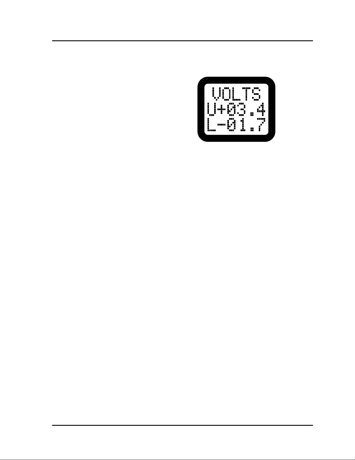
Voltage Set
Upper-voltage set point of
+3.4 V and a lower-voltage
set point −1.7 V
VOLTAGE-SET SCREEN
Function To set the upper- and lower-voltage set points.
From the OPERATE screen Press the display twice.
To the OPERATE screen Press the display six times or wait approximately twenty
seconds.
Defaults +10.0 V and +00.0 V.
Discussion The upper-voltage set point can be any voltage from
9.9 V to +10.0 V while the lower-voltage set point
−
can be any voltage from −10 V to +9.9 V.
Operation There are four possible characters to set on this screen.
When the screen is first displayed, the blinking cursor
is on the 1’s digit of the upper-voltage set point. Press
(and release) the encoder until the cursor is at the digit
to be changed. Then, rotate the encoder until that digit
is set. Continue until all the digits are set. Remember
that the two voltages cannot be closer to each other
than 0.1 V.
INPUT-SIGNAL SCREENS
There are three screens to filter and condition the input signal to enhance the performance
of the Model 441A. The first, PULSES/REVolution, eliminates input-signal error due to
periodic, repetitive variations or errors. The next two screens, INPUT SENSitivity and
INPUT B/W, work in conjunction with each other to provide the user nine combinations
of input conditioning for the input signal. See the Applications section for further discussion.
Pulses/Revolution Screen
Function To set the number of pulses of the input signal that
occur during one revolution (or cycle).
From the OPERATE screen Press the display three times.
3-7

Operation Model 441A
Figure 3-6
Pulses/Rev
P/R set ON and number of
pulses set to 96
To the OPERATE screen Press the display five times or wait approximately twenty
seconds.
Default OFF, 001.
Discussion The pulses/revolution filter can be set ON or OFF, and
the number of pulses can be set from 1 to 999. Note
that even though the PULSES/REV has been turned
ON, this function ceases to operate when the input signal
is outside the range of 1 Hz to 1 kHz (i. e. the time
between two consecutive input pulses is less than 1 ms
or greater than 1 s). It will reactivate automatically if
and when the input signal returns to within that range.
Once this digital filter has been turned ON or internally
reactivated, one revolution must occur before the output
of the Model 441A is averaged.
Operation Pressing the encoder moves the cursor from one char-
acter to the next, (ON or OFF is the first choice). Then
rotate the encoder for the number of pulses per cycle.
Figure 3-7
Input Sensitivity
Input sensitivity
set to MAX
Input-sensitivity Screen
Function To set the input-voltage sensitivity.
From the OPERATE screen Press the display four times.
To the OPERATE screen Press the display four times or wait approximately
twenty seconds.
Default MAX.
3-8

Model 441A Operation
Discussion The input sensitivity can be set to MIN, MID, or MAX.
Operation Since there is only one character to change on this
screen, the encoder push-button action has no function.
Simply rotate the encoder to select the desired sensitivity.
Figure 3-8
Input bandwidth
Input bandwidth
set to MID (midrange)
Input-B/W (Filter) Screen
Function To select the input filter.
From the OPERATE screen Press the display five times.
To the OPERATE screen Press the display three times or wait approximately
twenty seconds.
Default MAX.
Discussion The input bandwidth can be set to MIN, MID, or MAX.
Operation Since there is only one character to change on this
screen, the encoder push-button action has no function.
Simply rotate the encoder to select the desired filter.
Figure 3-9
Output filter
Output filter
cutoff frequency
of 100 Hz
OUTPUT-FILTER SCREEN
Function To set the output filter.
From the OPERATE screen Press the display six times.
To the OPERATE screen Press the display twice or wait approximately twenty
seconds.
Default WB (wideband).
3-9

Operation Model 441A
Discussion The filter can be set to 1 Hz, 10 Hz, 100 Hz, or WB,
which is approximately 1.5 kHz.
Operation Since there is only one character to change on this
screen, the encoder push-button action has no function.
Simply rotate the encoder to select the desired filter.
Figure 3-10
CAL screen
CAL “on”
and CAL frequency
set to 12.5 kHz
CAL SCREEN
Function To set the calibration frequency.
From the operate screen Press the display seven times.
To the operate screen Press the display once or wait approximately twenty
seconds.
Defaults OFF, 25000 Hz.
Discussion The calibration frequency is used in conjunction with
the upper and lower set points of frequency and voltage.
It simulates the frequency and puts out the corresponding
voltage when ON. For example, if the user has frequency
set points of 1 kHz and 2 kHz and voltage set points
of 1 V and 2 V, he or she may want to set a CAL
frequency of either the upper or lower frequency set
points or perhaps the midpoint, 1.5 kHz. This is not to
say that the cal frequency must be within the frequency
set points.
Operation First, set the CAL function to ON or OFF by rotating
the encoder, select the digit or digits to be set using the
push-button function of the encoder, and then set them
with the rotary function.
SECONDARY SCREENS
Access to these screens, VIEW ANGLE and ±10 V ALIGNMENT is by pressing and holding
the display while at any of the primary displays. The sequence is VIEW ANGLE, –10 V ALIGN-
MENT, and +10 V ALIGNMENT. Adjustment of VIEW ANGLE is discussed on Page 3-4.
3-10

Model 441A Operation
Figure 3-11
Adjust +10 V
screen used
to align the out-
put with internal
software
Ten-volt Alignment
Function The alignment screens allow the operator to align the
output of the Model 441A with its internal software using a voltmeter.
From the OPERATE screen Press and hold the display for more than one second
and then press the display once for negative 10 V alignment and twice for positive 10 V alignment.
To the OPERATE screen From the negative 10 V alignment screen, press the dis-
play twice; from the positive 10 V screen, once.
Default +000.
Operation When at the negative 10 V alignment screen, connect
a DMM to the output of the Model 441A and then using
the encoder, adjust the output for −10 V ±0.005 V. Next
press the display once to go to positive 10 V alignment
screen and adjust the encoder for +10 V ±0.005 V. The
three-digit number on each display is a reference number
for the convenience of the user. The user may want to
note the readings once the alignment is made. Then if
an alignment is required in the future and a voltmeter
is unavailable, the user can simply reset the numbers
to those noted above with confidence that the unit is
properly aligned.
There are four additional secondary screens: MEMORY ERROR, RESET, ALIGNMENT
REQUIRED, and a temporary screen seen only after a reset is made.
Figure 3-12
The ALIGNMENT
REQUIRED screen will
appear so long as ±10 V
alignment is necessary.
The displayed digits
are for factory use.
3-11
Operation Model 441A
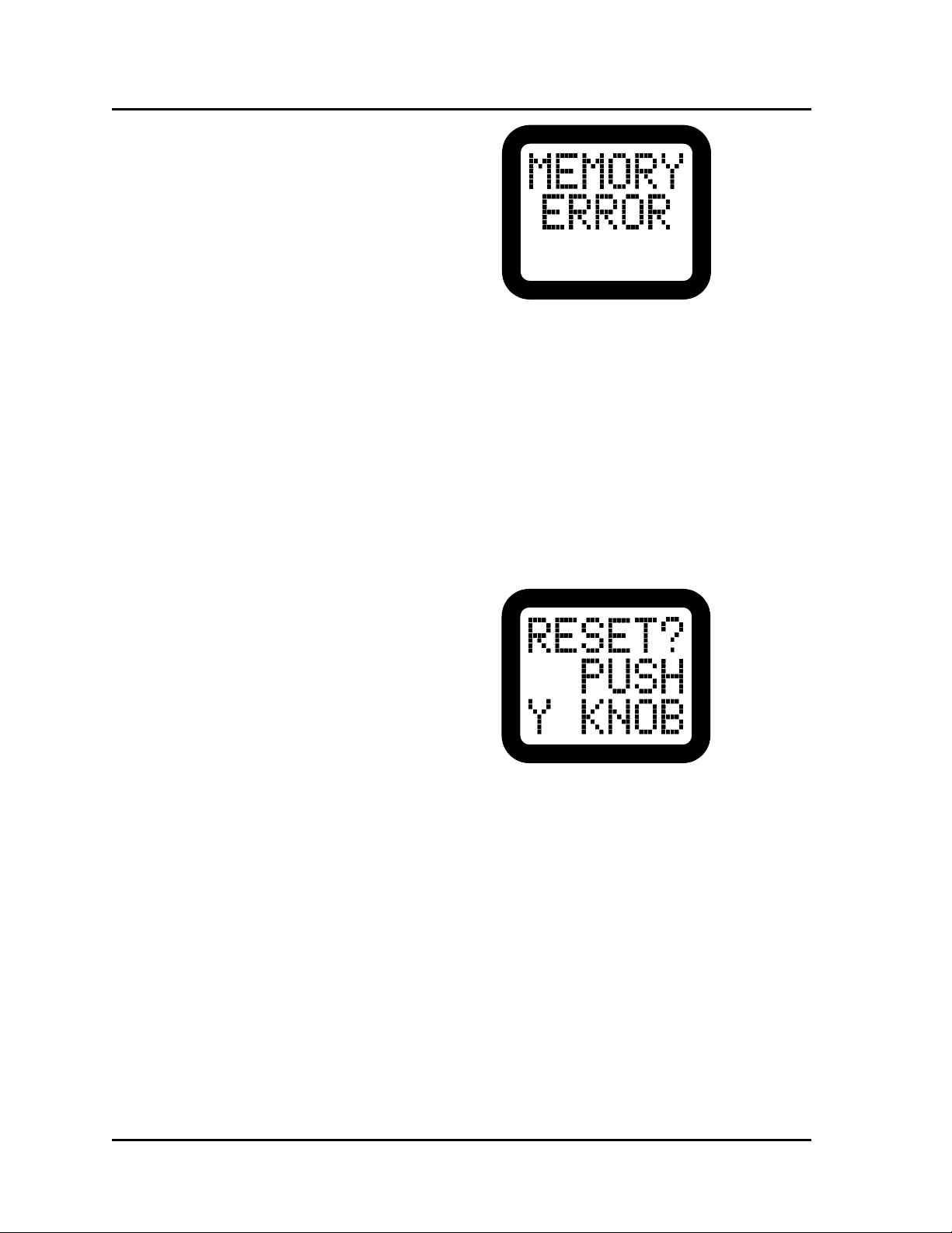
Figure 3-13
The MEMORY-ERROR
screen will appear
if an error in nonvolatile
memory occurs.
MEMORY ERROR is inaccessible by the user and will normally never be seen. As is
shown in Figure 3-1, each time the Model 441A is energized, nonvolatile memory is tested.
Normally, it will pass the test and will immediately display the OPERATE screen. However,
should a memory error occur, the MEMORY ERROR screen will be displayed. To advance
past this screen, press the display or press or turn the encoder. The Model 441A will then
restore the default settings (Table 3-2) and go to the ALIGNMENT REQUIRED screen.
Again the operator can press the display or press or turn the encoder, and the unit will
advance to the OPERATE screen. Until the two 10 V alignments are performed, the unit
will stop at the ALIGNMENT REQUIRED screen each time power is applied.
If the user chooses, the default settings can be restored by going to the RESET screen and
selecting Y (yes) PUSH KNOB.
Figure 3-14
Use the RESET
screen to restore
the default parameters.
Reset
Function To restore the default settings.
From the OPERATE screen Press and hold the display until VIEW ANGLE is dis-
played, press the display twice more (plus 10 V alignment), and then press and hold the encoder for one
second or more.
To return to the OPERATE
screen (without having
performed a reset)
To return to the OPERATE
screen (having performed
a reset)
Press the display when the screen displays N (no) PUSH
DISPlay or wait 20 seconds.
Press the encoder when the screen displays Y (yes)
PUSH KNOB. As shown in the operational-state dia-
gram, the operate screen is displayed only after a momentary RESET screen and the alignment-required
3-12

Model 441A Operation
screen has been cleared by pressing the display or pressing or turning the encoder.
Operation Rotate the encoder to select Y (yes) PUSH KNOB or
N (no) PUSH DISPlay.
Discussion Only when the user has selected Y PUSH KNOB and
has pressed the encoder will a reset be performed. Then
the unit will display the ALIGNMENT REQUIRED
screen, and the user can proceed as previously described.
ENCLOSURES
Model E408-1
The Model E408-1 is a single-unit mount designed to mount directly to a bulkhead or to a
DIN rail (Option D). It can be mounted on three of its six sides with screws (10-32 machine
screws are recommended) in any aspect. The installed unit can be right-side up or down
within the mount as well. A right-angle hooded DAM-15S connector is provided for cabling.
The hooded shell can be mounted right-side up or down, too, depending on where the user
would like the cabling to exit. Drawing 408-900 shows all unit dimensions as well as mounting
dimensions.
Model E408-6
The Model E408-6 enclosure is a six-channel bench-top unit, which will hold Models 352,
428, 441A, 441AL, and 451 in any combination. Being small, lightweight, and powered
either by ac or dc, the enclosure is well suited for use in the field as well as the laboratory.
Features
Inside the top cover, which is held on by four captive
•
screws, are terminals for each channel for bridge completion, CAL, and bridge balance (for Model 352).
Channel-input and dc-power connectors are PT series,
•
and output connectors are BNC. An ac power cord and
mating connectors for all but the BNC’s are provided.
Front-panel controls include power on-off (for ac and
•
externally applied dc); ALL ZERO for Model 428
equipped with autozero (Option O); and CAL with positions of +, −, and OPR (operate), which is functional
when a CAL resistor and any bridge configuration are
installed or connected. Calibration is input shunt calibration by means of electronically switching a customerinstalled CAL resistor in parallel with selected arms of
the bridge to produce either a plus or a minus calibration.
Also included are provisions for bridge balance for units
•
so equipped and output frequency-response control for
Model 352 amplifier-conditioners.
As with all Ectron enclosures, the Model E408-6 does
•
not degrade any plug-in specifications.
3-13

Operation Model 441A
Model E408-6Y has an internal 12 V dc power supply,
•
and the E408-6X has a power supply of 28 V dc.
When setting up the Model E408-6 for operation, refer
•
to either Drawing 408-600 (for 12 V dc systems) or
408-601 (28 V dc systems) at the rear of this manual
for settings of plug jumper W1 (W2 is not active when
using the Model 441A in this enclosure). Also depicted
are typical input configurations the customer may want
to use.
Model R408-14
The Model R408-14 enclosure is a 14-channel 3-
1
-inch-high,19-inch-wide rack-mount unit
⁄
2
that holds Models 352, 428, 441A, 441AL, and 451 in any combination. It also is powered
by either dc or ac and comes in both 12 V dc (Option Y) and 28 V dc (Option X) versions.
Features
Beneath the top cover are terminals for each channel
•
for bridge completion, CAL, and bridge balance (for
Model 352).
Channel-input and dc-power connectors are PT series,
•
and output connectors are BNC. An ac power cord and
mating connectors for all but the BNC’s are provided.
Front-panel controls include power on-off (for ac and
•
externally applied dc); ALL ZERO for Model 428
equipped with autozero (Option O); and CAL with positions of +, −, and OPR (operate), which is functional
when a CAL resistor and any bridge configuration are
installed or connected. Calibration is input shunt calibration by means of electronically switching a customerinstalled CAL resistor in parallel with selected arms of
the bridge to produce either a plus or a minus calibration.
Also included are provisions for bridge balance for units
•
so equipped and output frequency-response control for
Model 352 amplifier-conditioners.
3-14
As with all Ectron enclosures, the Model R408-14 does
•
not degrade the specifications of any plug-in.
Model R408-14Y has an internal 12 V dc power supply,
•
and the R408-14X has a power supply of 28 V dc.
When setting up the Model R408-14 for operation, refer
•
to either Drawing 408-605 (for 12 V dc systems) or
408-606 (28 V dc systems) at the rear of this manual
for settings of plug jumper W1 (W2 is not active when
using the Model 441A in this enclosure). Also depicted
are typical input configurations the customer may want
to use.

Section IV
Applications
GENERAL
To best understand how to apply the Model 441A, it is important to know some characteristics
of its design. This information is available in Section V, Theory of Operation, where some
of the features of the design as they apply to application of this product are covered.
INPUT-SIGNAL CONDITIONER
The job of the input-conditioner section of this instrument is to accommodate input signals
with a variety of waveforms, frequencies from 1 Hz to 50 kHz plus harmonics, and amplitudes
from 10 mV peak to 100 V peak. This must be accomplished such that the frequency integrity
of the input signal is carefully maintained, even while short-term frequency and amplitude
variations occur. Furthermore, the input must be adaptable to many signal sources and grounding conditions.
To minimize ground-loop problems the input was made differential and isolated from case
and power ground. Although signal levels are several-orders-of-magnitude greater than those
of transducer amplifiers, noise effects are still very important if accuracy and response are
required. This is because noise on the input signal causes unavoidable jitter in the conversion
process. (Filtering reduces this jitter but at a sacrifice of response time.)
Three controls are provided to improve conversion stability. These are a three-step inputsensitivity control, a three-step input-bandwidth control, and a digital periodic filter that
eliminates cyclic variations in the input signal.
An automatic-gain-control (AGC) circuit converts the input-frequency waveform to a waveform of relatively constant amplitude. Since zero crossings determine the action of the frequency-to-voltage converter, these must be carefully preserved in the signal conditioner.
Then a squaring circuit increases the rise and fall times of the waveform.
Since a sine wave does not have an abrupt wave front, frequency conversion for these signals
is not so accurate as for square or pulse waveforms. Thus, a low-amplitude sine-wave signal
will be more susceptible to noise and will generally show more noise on the output analog
signal as well as the frequency read-out on the display.
Square and pulse waveforms will give the most noise-free operation. The duty cycle of pulse
signals should be greater than about 5%. Minimum acceptable pulse width is approximately
5 µs. Although there is no minimum for rise or fall time, little is gained below about 0.6 µs.
INPUT SIGNAL, GROUNDING, AND SHIELDING
Four independent grounds exist within the Model 441A. As a result, flexibility exists in
adapting this unit to a variety of input signal sources. The available ground systems are:
• Input (two input leads and shield).
• Output (output high and low).
• Dc power (plus and common).
• Case.
4-1

Applications Model 441A
Proper use of these grounds will result in lower noise and more accurate data. (See the
paragraphs under uncertainty, resolution, and noise in this section.) However, incorrect grounding will increase noise and degrade data accuracy. Some grounding recommendations follow:
Input In any signal system, use only one ground point. This
applies to the input and output signal systems. The signal
input can be “floated off” ground to 100 V dc or peak
ac and grounded anywhere that suits the application.
The input-shield pin (Pin 9) should be tied to the signal-source common. Shielding and use of twisted-pair
leads are recommended if the input amplitude is below
100 mV or the electrical environment is poor.
Output The high- and low-output leads can and usually should
be grounded at the load device. Depending on the load
device, connecting this common to earth ground or dcpower-supply ground can minimize noise.
Power The negative of the dc power source should be connected
to earth or power-line ground. In Ectron enclosures, this
is accomplished by proper use of the third-wire-ground
pin on the power cord.
Case Case ground (Pin 5) should be connected to earth or
power ground. This is done in Ectron enclosures.
EMI PROTECTION
All connections to the converter go through emi-rfi filters to minimize the effects of rf noise.
The filter frequency coverage starts with about −3 dB of attenuation at 1 MHz, increasing
to −66 dB at 200 MHz and beyond. Emi-rfi filtering is particularly important in vehicle
testing, especially involving an engine where wideband emissions are generally high.
FREQUENCY-TO-ANALOG CONVERSION
The digital section receives the conditioned and shaped input-frequency signal. First, frequency-to-digital conversion takes place followed by digital-to-analog conversion. Both of
these digital-domain processes are governed by the user-selected frequency and voltage set
points.
OUTPUT ANALOG FILTER AND OUTPUT STAGE
To smooth the resulting analog signal, four user-selectable filter frequencies are available:
1 Hz, 10 Hz, and 100 Hz having second-order Bessel characteristics and a wideband (WB)
one-pole filter at approximately 1500 Hz. The analog output stage can drive loads at up to
±10 V at 10 mA. A short circuit on the output for an indefinite period will not harm the
instrument.
FREQUENCY AND VOLTAGE SET POINTS
The frequency set points determine the input frequency at which the upper- and lower-voltage
set points are reached. The frequency set points can be any frequency between 0 Hz and
50 kHz with a resolution of 1 Hz. The two frequency set points can be within 10 Hz.
4-2
Model 441A Applications
Similarly, the voltage set points determine the output voltages corresponding to the upperand lower-frequency set points, respectively. The voltage set points can be any voltage from
−10 V to +10 V with a resolution of 0.1 V. The two voltage set points can be within 0.1 V.
Table 4-1 illustrates converter operation with hypothetical frequency and voltage set points.
Table 4-1
Input Frequency vs Output Voltage (Example)
Frequency set points Voltage set points
(
)
Upper
Lower
f
2000 Hz
U
(
)
f
L
1000 Hz
Upper
Lower
Input Frequency Output Voltage Input Frequency Output Voltage
(
)
V
+
5 V
U
V
(
0
)
V
L
1000 0 3500
1500
2000
3000
2.5 900
+
5 500
+
10 0
+
10.5*
+
0.5
−
2.5
−
5
−
* The output limits at approximately ±11 V.
Should the application require it, the output can be set to provide a bipolar output (e.g., for
a certain frequency range the output can be set to go from −5.000 V to +5.000 V). Similarly,
the output voltage could be set to be all negative. Note that the higher frequency will always
produce the more positive output voltage.
Because the minimum difference between the upper- and lower-frequency settings is 10 Hz,
and the minimum difference between the upper- and lower-voltage settings is 0.1 V, it is
possible to set fU at 1000 Hz and fL at 990 Hz, VU to 1.0 V and VL = 0.9 V, thus giving a
frequency-to-voltage sensitivity of 100 Hz/V. Exactly the same results would be obtained if
the settings were fU = 1500 Hz, fL = 900 Hz, VU = 6 V, and VL = 0 V. The following section
shows that extreme settings can result in poor resolution and noise.
NOISE
In addition to frequency jitter of the input signal, noise at the output of the Model 441A
will be a combination of input signal noise, waveform character, signal amplitude, and instrument settings. For square and pulse waveforms, output noise should be well under the
10 mV p-p specification assuming sharp rise times and good pulse-to-pulse frequency and
phase stability. Ideally, rise times should be under 5 µs to utilize the extraordinary conversion
accuracy, resolution, and stability of this instrument. A further source of noise can be grounding problems of input and output signal circuits.
Despite the fact that the amplifier’s input is differential, input-to-output cross talk can exist
external to the amplifier. Good wiring practices should be followed to minimize this effect
(see Page 4-1, INPUT SIGNAL GROUNDING AND SHIELDING).
An additional source of input-to-output crosstalk is an inadequate case ground. All pins of
the connector incorporate emf-rfi filters. The capacitors associated with these filters connect
to case ground (Pin 5 on the DA connector). Consequently, if no case ground exists, signals
from one pin will be coupled to other pins by these capacitors. For example, if a sharp-rise
4-3

Applications Model 441A
Figure 4-1
Maximum Uncertainty for Various Frequencies
square-wave signal exists on the signal input pins, pulses will be seen on the analog output
signal unless a good case ground exists. Ectron enclosures provide such a ground assuming
input power, either ac or dc, includes a good ground. Note that neither the input nor output
filters of the Model 441A will have much effect on these feed-through pulses.
For any frequency-to-voltage converter with fast response, sine-wave signals are the most
difficult from which to produce a low-noise output. This is because the slightest noise will
cause jitter in the “wave to wave” timing.
If a 10 mV p-p sine wave has even 100 µV of amplitude noise, then timing errors can cause
the frequency conversion to produce volts of output noise when the frequency input is high
and the frequency set-points difference is small. Figures 4-4 and 4-5 indicate expected output
noise for “clean” sine-wave signals of 10 mV p-p and 1 V p-p, respectively.
To reduce the output noise under difficult input signal conditions, the operator should use
as much filtering as possible and should set a wide frequency-set-points difference. Another
possibility is to reverse the input leads to the unit. This may improve the waveform at the
transition point of the converter and produce less output noise.
4-4
Model 441A Applications
Figure 4-2
Worst-case Resolution for Various Frequencies
If the input waveform is sawtooth, then output noise will be best if the slow-rise portion of
the waveform is positive going, and the abrupt fall is negative going. This is true since the
internal conversion circuit of the Model 441A uses the fall time for triggering. However, if
the waveform is the reverse, slow fall and abrupt rise, simply reverse the frequency-input
leads. Since the input is differential, this reversal will not cause noise or ground-loop problems.
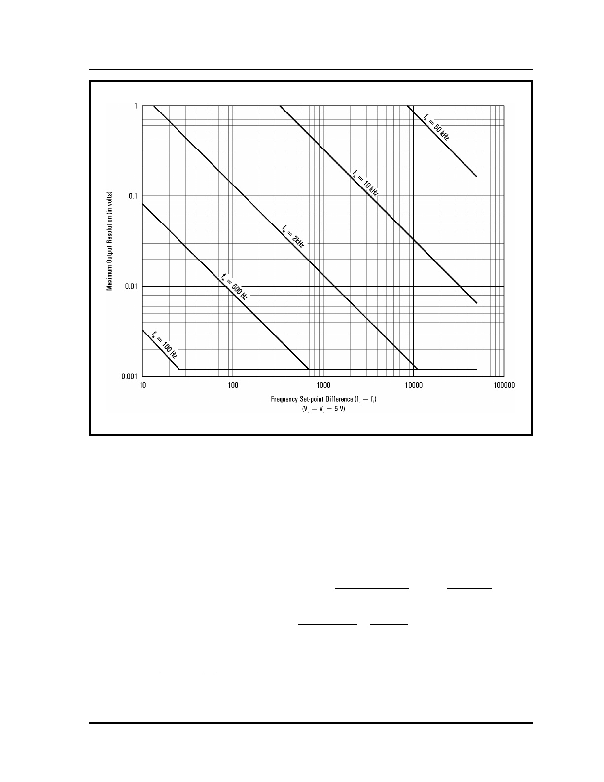
UNCERTAINTY AND RESOLUTION
10
×
6
)f
10
6
) −
VU − V
fU − f
in
f
L
Output analog uncertainty is within ± 0.00122 +
quencies less than 1 kHz, and ± 0.00122 +
(
1.5
× 106)F
f
in
(1.5 ×
2
(1.5 ×
and above. Output resolution for input frequencies of 1 kHz or below is the greater of
2
0.0012 V or
f
in
1.5 × 10
×
6
VU − VL
f
U
− f
, resolution for frequencies above 1 kHz is 0.0012 V
L
V
− VL
− f
in
in
L
for frequencies of 1 kHz
U
×
fU − f
for fre-
L
4-5

Applications Model 441A
Figure 4-3
Maximum of Uncertainty and Resolution for Various Frequencies
(Figures 4-1 and 4-2 Combined)
2
or
f
in
1500F
×
V
fU − f
U
− V
L
, and output analog noise is less than 10 mV p-p independent of
L
input frequency measured in a bandwidth of 0.1 Hz to 1 MHz assuming a clean, fast, zero-
1
crossing signal.
The preferred signal is a square wave or a pulse with fast fall times (the
internal detector operates on the negative-going portion of the waveform.) For slow-rise-time
signals including sine waves, output noise depends on input-signal amplitude and noise,
since accurate timing determination is hampered by noise.
Figures 4-1 through 4-5 illustrate the variation of uncertainty, resolution, and noise for an
output of 0 V to 5 V (VL to VU). Different input frequencies (fin) are plotted against frequency
set-points differences (f
− fL).
U
Figure 4-1 illustrates the effect on uncertainty of different input frequencies and with different
frequency-set-points difference (f
1
For the four equations,
V
are the upper and lower voltage settings; and
L
f
is the input frequency; F is
in
− fL). Output-voltage set points are assumed to be 0 V
U
f
f
/
, rounded down to the nearest integer;
1000
in
f
and
are the upper and lower frequency settings.
U
L
V
and
U
4-6

Model 441A Applications
Figure 4-4
Maximum Output Noise with a 10 mV Sine-wave Input
and +5 V. Note that for the plot for an input frequency of 10 kHz, uncertainty reaches
0.023 V when (fU − fL) reaches 100 Hz. This could be for an upper-frequency setting of
10,050 Hz and a lower-frequency setting of 9950 Hz. Even for a frequency setting difference
of 10 Hz, uncertainty at 10 kHz only reaches a total of 0.27 V out of a full scale of 0 V
to 5 V.
Figure 4-2 shows that resolution reaches a worst case of 0.015 V for input frequencies of
up to 2,000 Hz and a frequency set-points difference of 1000 Hz or higher. Again, output
voltage set points are 0 V and +5 V. However, as input frequency increases and the frequency
set-points difference decreases, resolution degrades. Fortunately, extreme sets of conditions
should seldom occur.
Figure 4-3 is a combination of Figures 4-1 and 4-2 to illustrate the worst case the user can
expect at extreme settings.
4-7
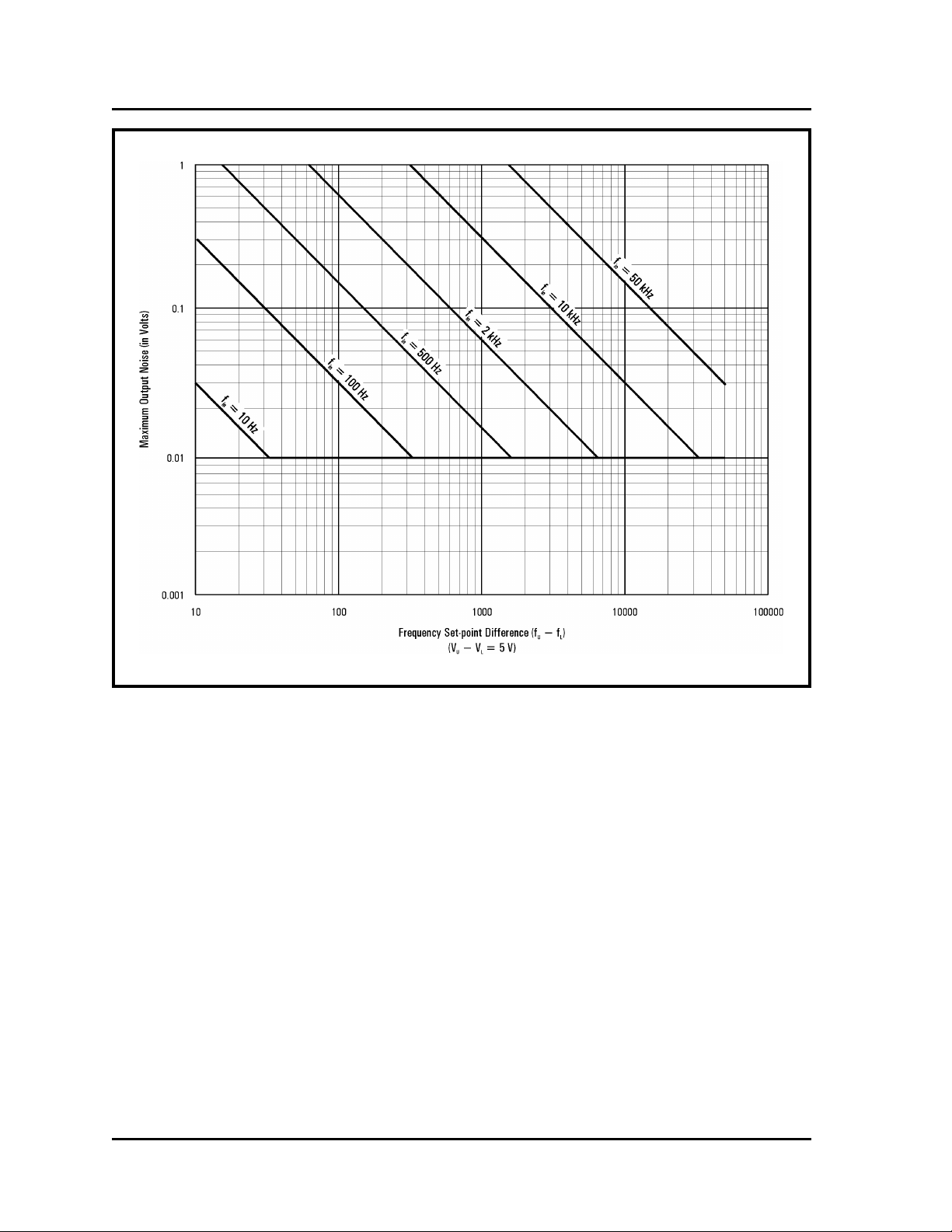
Applications Model 441A
Figure 4-5
Maximum Output Noise with a 1 V Sine-wave Input
FILTERING
There are three types of selectable filters in the Model 441A: input, output, and periodic-error.
The first two are analog low-pass filters, and the last is a digital filter. These filters have
the following characteristics and application.
Input Bandwidth Filter This filter is used to reduce noise on the input frequency
signal to provide reliable triggering. The screens are
labeled MIN, MID, and MAX bandwidth corresponding
to a single-pole low-pass filter with approximate corner
frequencies of 10 Hz (MIN), 500 Hz (MID), and
150 kHz (MAX). The proper setting for this filter depends on the noise frequencies and their relation to the
desired signal and is usually set by trial and error in
conjunction with the sensitivity control INPUT SEN-
Sitivity. Use the lowest bandwidth setting that provides
reliable triggering. Frequently, best operation is obtained
with the filter frequency set below that of the signal of
4-8

Model 441A Applications
interest. During setup, the lowest and highest signal frequencies should be tested for proper operation.
Output Filter This two-pole active filter is used to reduce noise of
the output analog signal. Corner frequencies are 1 Hz,
10 Hz, 100 Hz, and WB (approximately 1.5 kHz).
Since the lower the filter frequency the slower the response, a compromise must be made between noise and
response. (Response of the digital filter adds to the response of the analog output filter.) Table 4-2 indicates
the response to a step-frequency change for the four
filter frequencies assuming the digital filter is set to a
PULSES/REVolution of 001. In general, the user
should select the lowest filter setting consistent with the
response requirements of the application.
Table 4-2
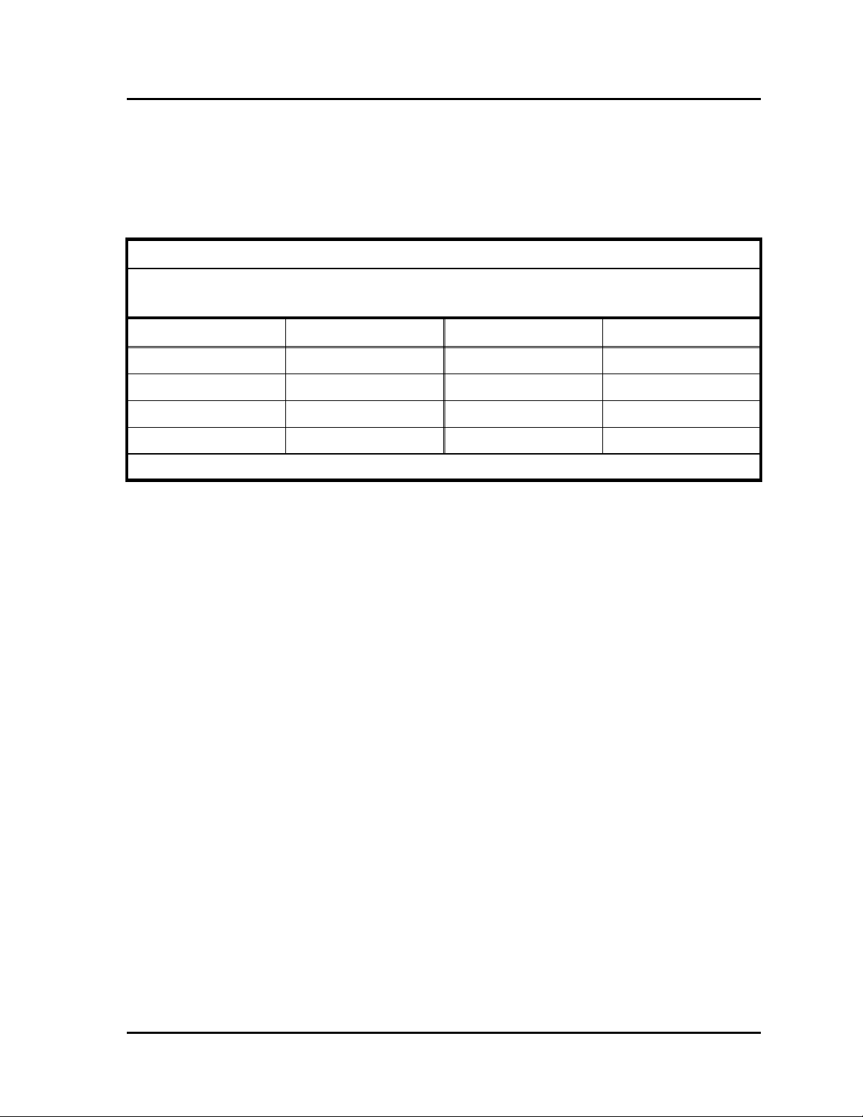
Response Time Versus Output Filter Setting
Output Filter in Hz
WB (1500) 0.005*
100 0.055*
10 0.5*
15.0*
1
⁄
* add
f
in
where
f
in
Approximate Response Time
in Seconds
is the input frequency
Digital Filter For operational frequencies up to 1 kHz, this unique
filter uses digital averaging of the converted input signal
to eliminate the unwanted effects of a signal whose frequency varies in a periodic manner. For example, the
output frequency of a paddle-wheel flow sensor usually
changes as the wheel rotates because the paddles are
not evenly spaced. If the sensor has eight paddles, its
output will consist of a repeating sequence of eight
pulses. If this signal is fed to a frequency-to-voltage
converter without this filtering, the output analog signal
will have a cyclic component with a period equal to
the period of rotation of the device. However, by using
the digital filter with an eight-pulse running average,
the period variation is averaged out and a much more
stable analog output is obtained.
Figure 4-6 illustrates the function of the digital filter
for a signal from an eight-paddle sensor. At first, the
unfiltered (stair-step) analog output varies about 5 V;
then the speed of rotation is increased so the signal
varies about 5.4 V. Keying in eight pulses per revolution
4-9

Applications Model 441A
Figure 4-6
Effects of the Digital (Periodic-error) Filter
changes the analog output to that shown by the smoothed
trace. Note that the second cycle of eight steps is changed
to a steady 5.0 V level. When the frequency abruptly
changes to the 5.4 V level, the digitally-averaged signal
linearly changes so that in eight steps, the 5.4 V level
is reached. As a result of the digital filter, the variation
(noise) caused by the eight-step cycle is eliminated. During and after the transition to a new level, eight-step
averaging continues.
The stair-step wave form during the frequency change
in Figure 4-6 is a result of the update rate of the unit,
which when period averaging is allowed, is longer than
1 ms. That is, period averaging only works below 1 kHz.
The filtering effect of digital averaging is useful in reducing random noise signals as well as periodic signals.
Response time will be reduced in direct proportion to
the Sample Count setting although response time will
change with input frequency. For example, for an eightcount sample period and an input frequency of 64 Hz
the response time (to reach final value) will be
For a frequency of 6400 Hz the response time will be
1
⁄
s.
800
1
⁄8 s.
4-10

Model 441A Applications
Figure 4-7
Filtering Scheme for ABS Testing
The Model 441A allows the user to set the number of
cycles of the period filter from 001 to 999 (001 being
the same as OFF) by setting the number as the PULSES
/ REVolution. (See Section III for instructions.)
For frequencies exceeding 1 kHz, the periodic filter is
automatically turned off. This means that anytime the
time interval between two pulses is less than 1 ms, the
filter is shut off (even though it has been activated at
the front panel by the user) and will automatically turn
on (provided it is programmed on by the user) if and
when the time interval exceeds 1 ms. Then, as soon as
the required number of pulses (determined by the pulsesper-revolution setting) has been received as input, the
output will again show the elimination of the periodic
error. The user who is operating near 1 kHz should be
mindful of this operation.
Applications for the period filter include flowmeters of
the turbine or propeller type, rotating-cup anemometers,
wheel-speed sensors of the cogged-wheel type (ABS
systems) used on automobiles, rotary optical encoders,
shaft torque detectors, etc. Usually, periodic errors are
caused by irregular spacing of the steps of the rotating
element of the device, but they can also be caused by
lack of concentricity between the rotating element and
the pick-off (run out).
Another application would be a jet turbine engine whose
rpm needs to be known or controlled exactly. A cogged
4-11
Applications Model 441A
Figure 4-8
Filter Circuit for ABS Testing
wheel rides on the engine shaft that has spacing irregularities. This causes a slight variation in the output pulse
spacing and would produce noise in the resulting analog
output of the Model 441A. This noise would prevent
knowing the exact rpm. If the wheel has 40 cogs, using
a PULSES / REVolution setting of 040 would eliminate the noise caused by the spacing irregularities.
Therefore, using digital averaging allows the output to
be as exact as the inherent high accuracy and stability
of the Model 441A.
SELECTABLE INPUT SENSITIVITY
This control adjusts the gain of the input amplifier and is useful when noise is causing
erratic triggering. This can occur when no signal is present or when the signal level is low.
Usually, the optimum setting of this control is made in conjunction with the input filter
setting. Gain decreases by a factor of approximately 6:1 from the MAX setting to the MID
setting. A further decrease of approximately 8:1 occurs between the MID setting and the
MIN setting.
RESPONSE TIME
Response to an abrupt frequency change is 0.005 s + 1⁄
band (f
is the new frequency). Thus, if the input frequency is 10 Hz and suddenly changes
new
to 1000 Hz, the analog output will assume the new value in less than 6 ms. For lower filter
frequencies,
5
(in seconds) must be added.
⁄
f
co
with the output filter set to wide-
f
new
UPDATE RATE
The update rate is 1 ms or 1⁄
, whichever is greater.
f
in
4-12

Model 441A Applications
Figure 4-9
Strip-chart Recording of ABS Action
LATENCY
Latency is the time required for the output to respond to a change in input frequency. Latency
in the Model 441A is within 1 ms of each falling edge of the input signal for input frequencies
above 1 kHz, and within 1 ms +
1
for frequencies below 1 kHz.
⁄
f
in
FRONT-PANEL INDICATION
The display on the front panel indicates the frequency of the incoming signal with a resolution
of five digits and the pulses per revolution setting of the periodic-error filter. Displaying the
input frequency serves several purposes during setup and operation of a test. First, it gives
the operator a “warm and fuzzy” feeling knowing that everything works. It confirms that
the pickup device is working and connections to the converter are correct. If the frequency
is approximately correct, it shows that the signal level is probably acceptable to the converter.
During the test, an operator can monitor the read-out to get a quick look at the frequency
data. The green front-panel LED will extinguish if no signal is present, and the display will
read 0.0000. If the input signal exceeds 50 kHz the read-out will continue to read correctly
until the frequency exceeds 63 kHz. Above this frequency, the read-out will show dashes.
(The analog output also will continue to be correct until it reaches approximately 11 V.)
The setting of periodic filter has also been selected for this screen because an incorrect
setting such as the wrong number of pulses per revolution increases noise as can using it
above 1 kHz.
CALIBRATION
The CALibration mode allows the operator to set a calibration signal from 0 Hz to 50 kHz
in 1 Hz increments. When CAL is enabled, the analog output assumes a voltage value of
the CAL frequency in accordance with the frequency and voltage set points. The calibration
circuit does not test the input-signal-conditioning circuitry and ignores any input signal.
To turn on the calibration signal, go to the CAL screen, adjust the frequency, and set OFF-ON
to ON. At this time, the output will assume the analog value corresponding to the frequency
and voltage set conditions. This output and the CAL screen will remain until it is exited or
the CAL is toggled OFF.
4-13

Applications Model 441A
The CAL mode can be used as a highly accurate linearity check of the equipment that
follows the Model 441A. First, perform the voltage alignment as described in Section III,
and then step the calibration settings over the range of interest, perhaps from zero to full
scale in 10% increments. This test should produce a system linearity check within an
uncertainty of 0.1% of full scale.
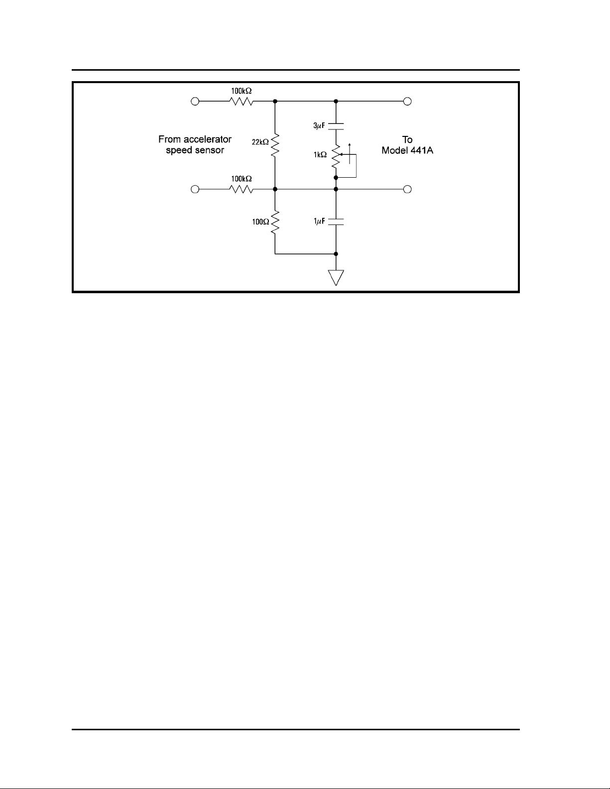
VEHICLE APPLICATIONS
Because the modern automobile generates a great variety of sometimes intense noise signals,
acquiring good data, especially from low-level signals, requires extraordinary measures. Vehicle noise usually involves both electromagnetic and electrostatic signals covering the spectrum from subaudio to many megahertz frequencies. Signal and power leads usually require
filtering for both normal-mode and common-mode components ahead of the instrumentation
involved. Leads carrying battery power will be “ contaminated” when exposed to enginecompartment noise for even a few feet unless appropriate precautions are taken.
ABS signals
2
The following example involves using the Model 441A
to monitor the wheel speed sensor signals of an antilock
brake system (ABS) on a vehicle. These signals, approximately 10 Hz per mile/hour of speed, are typically
generated by a magnetic pickup producing a sinusoidal
signal used by the ABS system. Therefore, the signal
varies from 0 Hz to 1000 Hz for speeds from zero to
100 mph. The signal amplitude increases with speed
from about 30 mV at 10 mph to 3 V at 100 mph. This
signal would be ideal for the Model 441A except for
the noise, both common mode and normal mode, that
has an amplitude of from 1 V to 3 V p-p. Obviously,
without filtering these signals, the output of the converter
would not be very usable, especially at lower speeds.
Because of noise on the power leads in a vehicle, the
recommended power source is a separate battery. If vehicle battery power is used, it is mandatory that additional filtering be incorporated in the power leads. The
filter should be located adjacent to the enclosure of the
frequency-to-voltage converters, and it should have
60 dB of attenuation from 10 kHz up to several megahertz. Both plus and common leads should be filtered
with respect to a good chassis ground.
Figure 4-7 shows a recommended wiring diagram of an
Ectron Model E408-6 enclosure with Model 441A frequency-to-voltage converters. Power is from a separate
battery. Adjustment of input filter and sensitivity should
2
The ABS system used for these tests involved General Motors Pontiac and Buick cars using the ITT/Teves
ABS. Although much of the information given here will apply to other ABS, there may be differences. It is
believed that connecting the Model 441A to the ABS signals will not affect operation of the standard ABS;
however, no guarantee of this can be made. Therefore, operation of the vehicle should be carefully tested after
any installation of this sort. These tests were performed using a Model 441. Using a Model 441A, the results
should be better than those shown because of the action of the input filter and response features of the newer
product.
4-14

Model 441A Applications
be made to provide optimum operation for the range of
speeds involved. The filter shown in Figure 4-7 can be
added ahead of the input to the Model 441A. Figure 4-8
shows a noise filter and attenuator that can be added
ahead of each Model 441A. The bridge-completion terminals of the Model E408-6 can be used for mounting
components of this filter. Note that the noise filter has
different characteristics for differential signals than for
common-mode signals.
Best results were obtained feeding the ABS signals
through an active input-signal conditioner that involved
filtering and pulse-shaping circuits ahead of the
Model 441A. Figure 4-9 shows a recording obtained at
the factory during these tests. Ectron engineers are available for consultation on specific applications.
4-15

Applications Model 441A
4-16
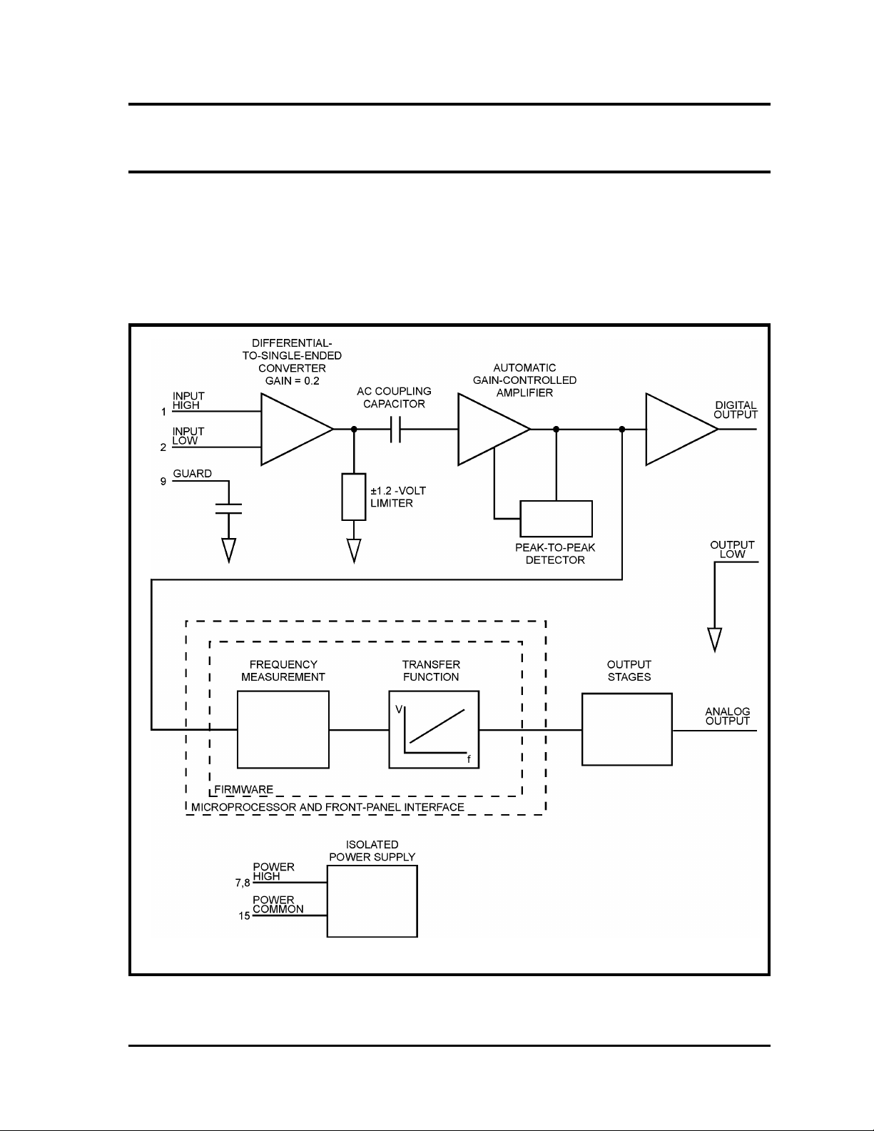
Section V
Theory of Operation
GENERAL
This discussion is organized to follow the signal flow, and as such describes the hardware
signal conditioning first, then the firmware, and then the hardware output stages. The powersupply discussion is placed after the signal-flow discussion. Refer to Figure 5-1, the block
diagram of the Model 441A.
Figure 5-1
Model 441A Block Diagram
5-1

Theory of Operation Model 441A
SIGNAL CONDITIONING (HARDWARE)
The two signal inputs feed a differential amplifier with a gain of 0.2, the single-ended output
of which is limited to approximately 1.2 V. Therefore, input voltages in excess of about 7 V
are limited at the output of this stage. This limiting does not affect the input impedance of
the Model 441A.
After the limiting stage, the signal passes through an ac-coupling capacitor, which removes
any dc component of the signal.
The signal next feeds through an amplifier, the gain of which is automatically controlled to
keep the peak-to-peak voltage of its output at a constant level. This ensures that input signals
of varying levels will be properly detected.
The signal then feeds to the microcontroller, which detects high-to-low transitions. High-tolow transitions are detected since many signal sources produce faster fall times than rise
times. When the input signal contains significant noise, any uncertainty in transition detection
results in uncertainty in frequency measurement. Slow transition times can cause transitiondetection uncertainties when the signal contains noise.
FREQUENCY MEASUREMENT (FIRMWARE)
Frequency measurement is based on the time period between high-to-low transitions of the
input signal. If the period of time between high-to-low transitions of the input signal is
greater than one millisecond, frequency is determined by taking the reciprocal of each signal
period. If the period of time is less than one millisecond, high-to-low transitions are accumulated until one millisecond has elapsed. Frequency is then determined by dividing the
number of transitions accumulated by the period of time required to accumulate those transitions. Granularity in period measurement is 667 ns, and the frequency is measured no
faster than once per millisecond.
TRANSFER FUNCTION (FIRMWARE)
Once the frequency has been determined, output scaling and offset must be applied to determine the proper output voltage.
First, the measured frequency is subtracted from the lower-frequency set-point. Then, that
difference is multiplied by the difference between the upper- and lower-voltage set-points,
and then that value is divided by the difference between the upper- and lower-frequency set
points. A correction factor is added to compensate output-stage component variations, and
the resulting value is fed to the output DAC (digital-to-analog converter). This correction
factor is determined by the plus- and minus-ten-volt alignment made during setup.
The firmware has the capability of performing the entire process 1000 times per second, so
the output voltage will properly represent the frequency of a particular cycle of the input
signal approximately one millisecond after a low-to-high transition of the signal (for input
signals of one millisecond or greater period).
OUTPUT STAGES (HARDWARE)
The output stages consist of a 14-bit DAC, an analog filter, and an output driver. These
circuits provide an output voltage range of approximately plus and minus eleven volts. The
filter is low-pass, two-pole, with Bessel characteristics; and is factory set to 1 Hz, 10 Hz,
and 100 Hz cutoff frequencies. The wideband position available from the front panel sub-
5-2

Model 441A Theory of Operation
stitutes a single-pole low-pass filter set to approximately 1500 Hz. The output driver provides
low-impedance outputs and is limited to approximately 20 milliamperes of output current.
POWER SUPPLIES (HARDWARE)
The Ectron Model 441A contains an isolated switching power supply which runs at approximately 20 kHz. All internal circuitry operates from this module, which is transformer coupled
to provide excellent isolation from the user’s power supply.
5-3

Theory of Operation Model 441A
5-4

Section VI
Alignment and Calibration
This section details the alignment and testing required to verify the proper performance of
the Model 441A. The basic alignment and calibration procedure is presented first, followed
by optional additional tests that the user may choose to perform. A blank calibration test
report is also included at the end of the section. Before proceeding, the operator should
become familiar with the operation of the Model 441A.
EQUIPMENT REQUIRED
Basic Alignment and Calibration
DMM
Oscilloscope
Function generator
Frequency meter
(if necessary)
Power supply
Mating connector
Switch
Additional Tests (Optional)
Agilent Model 34401A or equivalent. An equivalent
must have at least 0.01% accuracy in the range of 0 V
dc to 10 V dc.
Tektronix Model 7603 (with Model 7A13 vertical and
Model 7B53A horizontal plug-in’s) or equivalent.
Wavetek Model 188 or equivalent.
Needed if not already present in the DMM being used,
and if the function generator does not provide a precise
reading of the frequency.
Any (10.5 V dc to 32 V dc with at least a 200 mA
output).
Fifteen-pin (female) Type D subminiature such as a
DA-15S or a DAM-15S.
One single-pole single-throw toggle switch. The test
technician can forego the use of this switch, but it does
make the tests easier to perform.
Switch
PRE-CALIBRATION
Setup
One double-pole double-throw toggle switch. The test
technician can forego the use of this switch, but it does
make the tests easier to perform.
Connect the Model 441A as shown in Figure 6-1. Set
the power supply to any voltage from 10.5 V dc to
32 V dc and set S1 to On.
When the Model 441A is turned on, the
screen will normally appear. If
instead, adjust either of the front-panel controls to go
to the
OPERATE
screen.
ALIGN REQ’D
OPERATE
appears
6-1
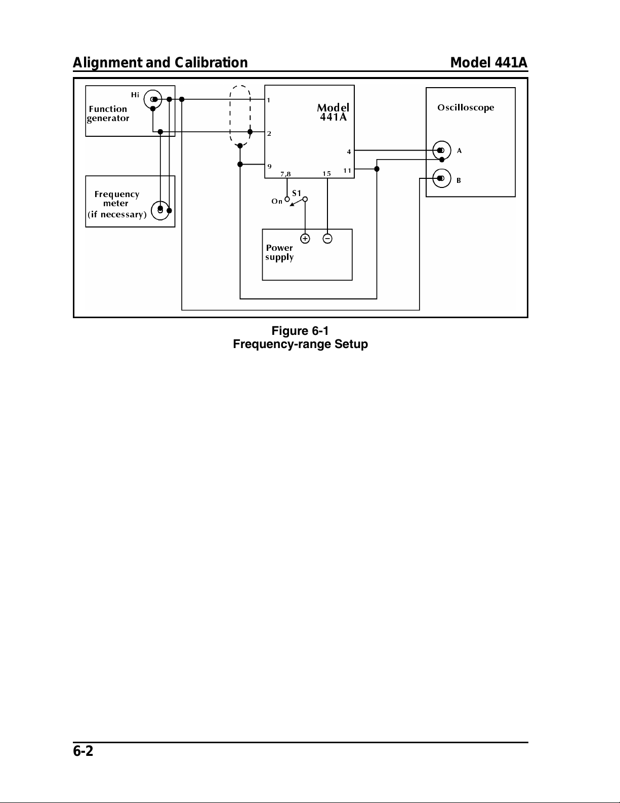
Alignment and Calibration Model 441A
+L
+L
0RGHO
$
2Q
Figure 6-1
Frequency-range Setup
$
%
Frequency Range Press the display once to go to FREQUENCY. Set the
Upper frequency to 50000 and the Lower frequency to
00000.
Press the display again to go to VOLTS. Set the Upper
voltage to +10.0 and the Lower voltage to +00.0.
Press the display six times (or wait approximately twenty
seconds) to return to OPERATE.
Set the function generator for a 50 kHz square wave of
5 V p-p. Verify the waveform is present on the oscilloscope.
Increase the frequency on the function generator until
the waveform disappears on the oscilloscope. Record
the highest frequency for which the Model 441A produces an output. If needed, use the frequency meter to
determine the exact frequency.
Press the display once to go to FREQUENCY. Set the
Upper frequency to 00001.
Press the display seven times (or wait approximately
twenty seconds) to return to OPERATE.
6-2
Set the function generator to 1 Hz. Verify the Model
441A registers the frequency.
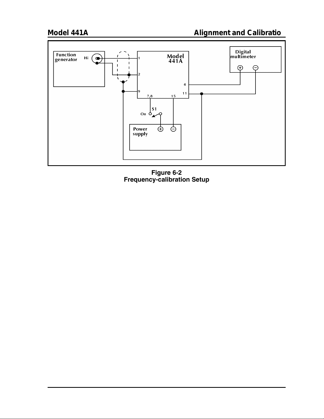
Model 441A Alignment and Calibration
+L
0RGHO
$
2Q
Figure 6-2
Frequency-calibration Setup
Reduce the frequency on the function generator until
the Model 441A no longer registers the input. (The reading will alternate between --- and 0.) Record the minimum frequency.
Frequency Calibration Connect the Model 441A as shown in Figure 6-2 and
set S1 to On.
Press the display once to go to FREQUENCY. Set the
Upper frequency to 01000 and the Lower frequency to
00000.
Press the display seven times (or wait approximately
twenty seconds) to return to OPERATE.
Set the function generator to 1 kHz.
When the DMM’s reading stabilizes, record the voltage.
Press the display once to go to FREQUENCY. Set the
Upper frequency to 50000.
Press the display seven times (or wait approximately
twenty seconds) to return to OPERATE.
Set the function generator to 50 kHz.
When the DMM’s reading stabilizes, record the voltage.
6-3

Alignment and Calibration Model 441A
2Q
0RGHO
$
Figure 6-3
Alignment
ALIGNMENT
Setup Connect the Model 441A as shown in Figure 6-3 and
set S1 to On.
Screen Adjustment From the OPERATE screen, press and hold the dis-
play/push button for one second to activate the
VIEW ANGLE screen. Adjust the encoder counterclockwise and clockwise to verify the view angle is
adjustable in both directions. Turning it clockwise darkens the screen and counterclockwise lightens it. When
finished, set the knob for the best viewing contrast.
Voltage Alignment While still at VIEW ANGLE, press the display once
to go to ADJUST −10 V. Adjust the encoder until
−10.000 V ±0.005 V is obtained on the DMM. The
three digits on this display (maximum range of ±750
counts) are provided as a reference if needed. The least
count is ≈1.3 mV. Record the DMM reading.
Press the display again to go to ADJUST +10 V. Rotate
the encoder until the DMM reads +10.000 V ±0.005 V.
The three digits on this display (maximum range of
±750 counts) are provided as a reference if needed. The
least count is ≈1.3 mV. Record the DMM reading.
6-4
Press the display again to the return to the OPERATE
screen.

Model 441A Alignment and Calibration
+L
/R
$
%
2Q
0RGHO
$
Figure 6-4
Optional Tests
POST-CALIBRATION
Follow the same procedure as given above for pre-calibration. This completes the alignment
and calibration of the Model 441A.
OPTIONAL CALIBRATION TESTS
Connect the Model 441A as shown in Figure 6-4 and set S1 to On.
Zero in, zero out From OPERATE, press the display once to go to FRE-
QUENCY. Set the Upper frequency to 50000 and the
Lower frequency to 00000.
Press the display again to go to VOLTS. Set the Upper
voltage to +10.0 and the Lower voltage to +00.0.
Press the display twice more to go to INPUT SENS
(The OUTPUT FILTER need not be set at this time.)
and rotate the encoder to display MAX.
Press the display again to go to INPUT B/W and again
rotate the encoder to display MAX.
Press the display twice (or wait approximately twenty
seconds) to return to OPERATE.
With S2 at 1, the output of the Model 441A, as read
on the DMM, should be 0 V ±0.005 V, and the green
light should be out.
6-5

Alignment and Calibration Model 441A
Sensitivity and AGC Set the function generator for a 5 Hz square wave. Ad-
just its output for 20 mV p-p as viewed on the oscilloscope. Set S2 to 2. The frequency displayed should
be approximately 5.0000.
Repeat the previous paragraph with the function-generator frequency set to 50 kHz. The frequency displayed
should be approximately 50000.
Set INPUT SENS to the settings listed in Table 6-1
and repeat the above sensitivity tests.
Repeat the previous paragraph with the function generator output adjusted to 20 V p-p. (You will have to
move to the Hi Output on the function generator.) The
frequency displayed should remain the same (approximately 50000).
Digital Output Connect an oscilloscope to the digital output (Pin 3)
and verify that the output is a 0 V to 5 V square wave
at the input frequency.
Table 6-1
Input Sensitivity
INPUT SENS INPUT VOLTAGE (p-p)
MAX 20 mV
MID 80 mV
MIN 600 mV
6-6

Model 441A Alignment and Calibration
Ectron Model 441A Calibration Test Report
Customer ___________________________ Date ________________
Address ___________________________ Serial Number ________________
___________________________ Report Number ________________
___________________________
Measurement Specification
PRE-CALIBRATION
Frequency Range Max ______________kHz >50 kHz
Min ______________Hz <1 Hz
Frequency Calibration
50 kHz ______________V 10 V ±0.0079 V
1 kHz ______________V 10 V ±0.0079 V
ALIGNMENT
Frequency Range
+10 V ______________V +10 V ±0.005 V
−10 V ______________V −10 V ±0.005 V
POST-CALIBRATION
Frequency Range Max ______________kHz >50 kHz
Min ______________Hz <1 Hz
Frequency Calibration
Temperature: ________°C Relative Humidity: _________%
Remarks:
50 kHz ______________V 10 V ±0.0079 V
1 kHz ______________V 10 V ±0.0079 V
Technician: _______________________ Inspection:
EQUIPMENT USED
Manufacturer Model Serial Number Cal Date Next Cal Due
6-7

Alignment and Calibration Model 441A
6-8

Section VII
Parts Lists
NAMES OF MANUFACTURERS
Table 7-1 lists the manufacturers of the components used by Ectron in the products for
which parts lists and schematics are provided. They are listed numerically for easy cross
reference to the parts lists.
Table 7-1
List of Manufacturers
Number Manufacturer Number Manufacturer
00027 Allen-Bradley Co. 00726 Rohm
00044 Amphenol 00763 Samtec
00060 Aries Electronics 00808 Siliconix Inc.
00074 Augat Interconnection 00834 Sprague Electric Co.
00091 Bendix Corp. 00845 Standard Power Inc.
00127 Bussmann Div. 00863 Switchcraft Inc.
00128 C&K Components Inc. 00949 Useco
00166 Circuit Assembly Corp. 00987 Winslow International
00206 Data Display Products 01094 Central Semiconductor
00336 Fairchild 01152 TRW-cinch
00464 ITT Cannon 01164 PEM
00493 Kemet, Union Carbide Corp 01166 Kulka Smith
00503 KOA Speer Electronics 01176 Belden
00532 Littelfuse Inc. 01177 Keystone
00564 Philips 01230 Ectron Corporation
00616 Motorola Semiconductor 01264 IRC (Int’l. Resistive Co.)
00628 National Semiconductor 01302 Elco (Cosel)
7-1

Parts Lists Model 441A
MODEL E408-6 ENCLOSURE
(Drawings 408-600 and 408-601)
REFERENCE DESIGNATOR DESCRIPTION MFR MANUFACTURER’S P/N ECTRON P/N
C1,C2,C3 CAPACITOR, 4.7UF/35V TANTALUM 00834 199D475X9035CA2 1-444700-1
C4 CAPACITOR, 4.7UF/50V CERAMIC 00493 C340C475M5U5CA 1-444709-0
CR1, CR2 DIODE, SIGNAL 01094 1N457 1-190457-0
CR3,CR4,CR6,CR7 DIODE, SIGNAL 00628 1N4148 1-194148-0
CR5 ZENER, 11V 11.5MA 500MW 00616 1N962B 1-190962-0
CR8 DIODE, POWER 00336 1N4002 1-194002-0
DS1 LAMP 00206 91W-EWR24H-CR0 4-121007-0
F1 FUSE, 1.5A NORMAL BLOW 00532 31201.5 2-161500-0
F2 FUSE, 1A SLOW BLOW 00532 313001 2-161000-1
J1-J6 CONNECTOR, 6-PIN 00091 PT02A-10-6S 1-310506-1
J7 CONNECTOR, 3-PIN 00091 PT02A-12-3P 1-310103-0
J8 RECEPTACLE, POWER 00863 EAC-309 3-840043-0
J9-J14 CONNECTOR, 15-PIN D 01152 DA-15-SV 1-310015-6
J15-J20 CONNECTOR, BNC 00044 31-010 1-311102-0
P1-P6 CONNECTOR, 6-PIN 00091 PT06A-10-6P(SR) 1-310506-0
P7 CONNECTOR, 3-PIN 00091 PTO6A-12-3S(SR) 1-310103-1
PS1, OPTION X POWER SUPPLY, 28 V 01302 R50U-24-N 5-120026-0
PS1, OPTION Y POWER SUPPLY, 12 V 01302 R50U-12-N 5-120025-0
Q1,Q2 FET, MOS 1.2-OHM 00808 VN0300L 1-240030-0
Q3 TRANSISTOR, PNP 00628 2N3702 1-213702-0
R5 JUMPER
R6,R7 RESISTOR, 1MEG/5% 1/4W 00564 5043EM1M000JB 6-174100-0
R8 RESISTOR, 470 OHM 5% 2W 01264 SPH 470 OHM 5% 2W 6-200470-0
R9 RESISTOR, 15K 1/4W 5% 00564 5043CX15K00J 6-172150-0
R10 RESISTOR, 100/5% 1/4W 00564 5043CX100R0J 6-170100-0
S1 SWITCH, TOGGLE 00128 7203-K-Z-G-E 7-110059-0
S2 SWITCH, PUSHBUTTON 00128 8121-J83-Z-G-E-3-2 7-120012-0
S3 SWITCH, TOGGLE 00128 7103-K-Z-G-E 7-110048-0
U1 IC 00808 7661CJ 1-147661-0
XF1,XF2 FUSEHOLDER 00532 342004 2-170006-0
W1, W2 JUMPER, PLUG 00166 CA-02-SJOB 1-319921-0
FOR TOP COVER SCREW, 6-32 CAPTIVE PANEL 01164 PS10-632-40 3-905032-1
FERRULE 01166 1670 3-905010-0
FOOT 01166 2192 3-840008-0
HANDLE 00949 B1073-12 BRASS CHRM PLT 3-820019-0
POWER CORD, USA/CANADA 01176 17250B 3-840026-0
7-2

Model 441A Parts Lists
MODEL R408-14 ENCLOSURE
(Drawings 408-605 and 408-606)
REFERENCE DESIGNATOR DESCRIPTION MFR MANUFACTURER’S P/N ECTRON P/N
C1, C2, C3 CAPACITOR, 4.7UF/35V TANTALUM 00834 199D475X9035CA2 1-444700-1
C4 CAPACITOR, 4.7UF/50V CERAMIC 00493 C340C475M5U5CA 1-444709-0
CR1, CR2 DIODE, SIGNAL 01094 1N457 1-190457-0
CR3, CR4, CR6, CR7 DIODE, SIGNAL 00628 1N4148 1-194148-0
CR5 ZENER, 11V 11.5MA 500MW 00616 1N962B 1-190962-0
CR8 DIODE, POWER 00336 1N4002 1-194002-0
DS1 LAMP 12-40V 00206 91W-EWR24H-CR0 4-121007-0
F1 FUSE, 5A/32V 3AG 00127 BK/AGC-5X 2-165000-0
F2 FUSE, 1A/25OV 3AG SLOBLO 00532 313001 2-161000-1
J1-J14 CONNECTOR, 6-PIN 00091 PT02A-10-6S 1-310506-1
J15-J28 CONNECTOR, BNC 00044 31-010 1-311102-0
J29-J42 CONNECTOR, 15-PIN 01152 DA-15-SV 1-310015-6
J43 CONNECTOR, 3-P 00091 PT02A-12-3P 1-310103-0
J44 RECEPTACLE, POWER 00863 EAC-309 3-840043-0
P1-P14 CONNECTOR, 6-PIN 00091 PT06A-10-6P(SR) 1-310506-0
P43 CONNECTOR, 3-PIN 00091 PTO6A-12-3S(SR) 1-310103-1
PS1, OPTION Y POWER SUPPLY 01302 R50U-12-N 5-120025-0
PS1, OPTION X POWER SUPPLY 01302 R50U-24-N 5-120026-0
Q1, Q2 FET, MOS VN 30V 1.2-OHM 00808 VN0300L 1-240030-0
Q3 TRANSISTOR, PNP 00628 2N3702 1-213702-0
R5 JUMPER
R6 RESISTOR, 1MEG 1/4W 5% 00564 5043EM1M000JB 6-174100-0
R9 RESISTOR, 15K 1/4W 5% 00564 5043CX15K00J 6-172150-0
R10 RESISTOR, 100 1/4W 5% 00564 5043CX100R0J 6-170100-0
S1 SWITCH, TOGGLE 00128 7303KYZGE 7-110024-0
S2 SWITCH, PUSH-BUTTON 00128 8125SHZBE 7-120002-0
S3 SWITCH, TOGGLE 00128 7103KZGE 7-110048-0
U1 IC, VOLTAGE CONVERTER 00808 7661CJ 1-147661-0
W1, W2 JUMPER 00166 CA-02-SJOB 1-319921-0
XF1, XF2 FUSEHOLDER 00532 342004 2-170006-0
FERRULE 01166 1670 3-905010-0
GROMMET, 3/8DIA 7/16MOUNT 01166 91107 3-801412-0
HANDLE, 3 INCH MOD R418-7 01166 1622 OR 1620 3-820002-0
POWER CORD, USA AND CANADA 01176 17250B 3-840026-0
7-3

Parts Lists Model 441A
7-4
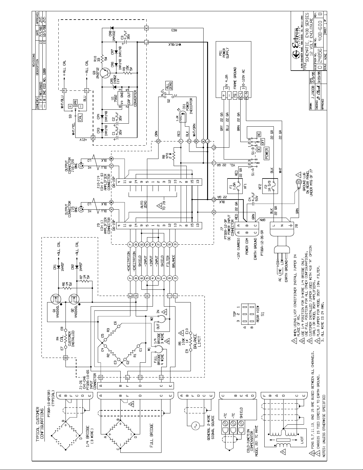


C3
4.7µF
35V
ZERO
AUTO
SHIELD
- INPUT
-EXCITATION
+EXCITATION
2
- INPUT
+ INPUT
TO J9
SHIELD
BALANCE
OUT
W2
GROUND LUG
ON REAR PANEL
UNDER MTG OF J43
4
IN
J43
PT02A-12-3P
CONNECTOR
DC POWER INPUT
+12V (UNREG)
SR
3S
12
-
POWER COM
PT06A
EARTH GROUND
LOW
HIGH
AC LINE
EARTH GROUND
R4
E8
CAL
E7
INSTALLED
CUSTOMER
J1-J14
CH1-CH14
PT02A-10-6S
INPUT
CONNECTOR
W1
1/4
BRIDGE
FULL
BRIDGE
6
3 WIRE
4 WIRE
R5
7
100K
E9 1% E10
S2
LIMIT
BALANCE
WHT/ORN 24GA
ORN 24GA
TO CIRCLE S
TO SQUARE N
WHT/YEL 24GA
WHT/BLU 24GA
TO SQUARE M
TO CIRCLE R
S3
YEL 22GA
BLU 24GA
TO SQUARE P
RED 22GA
TO F1
TO PS1+
GRY 22GA
TO CIRCLE T
BRN 22GA
TO PS1-ACL
YEL 22GA
TO CIRCLE U
REAR VIEW
TO XF2
BLK 22GA
S1


B
A
(TYPICAL)
PT06A-10-6P(SR)
B
F
CH1-CH6
PT02A-10-6S
INPUT
E
A
CONNECTOR
A
J1-J14
F
C
D
B
B
B
D
F
D
5
E
C
E
C
CONFIGURATIONS
TYPICAL CUSTOMER
D
1/4 BRIDGE
(3 WIRE)
A
D
C
FULL BRIDGE

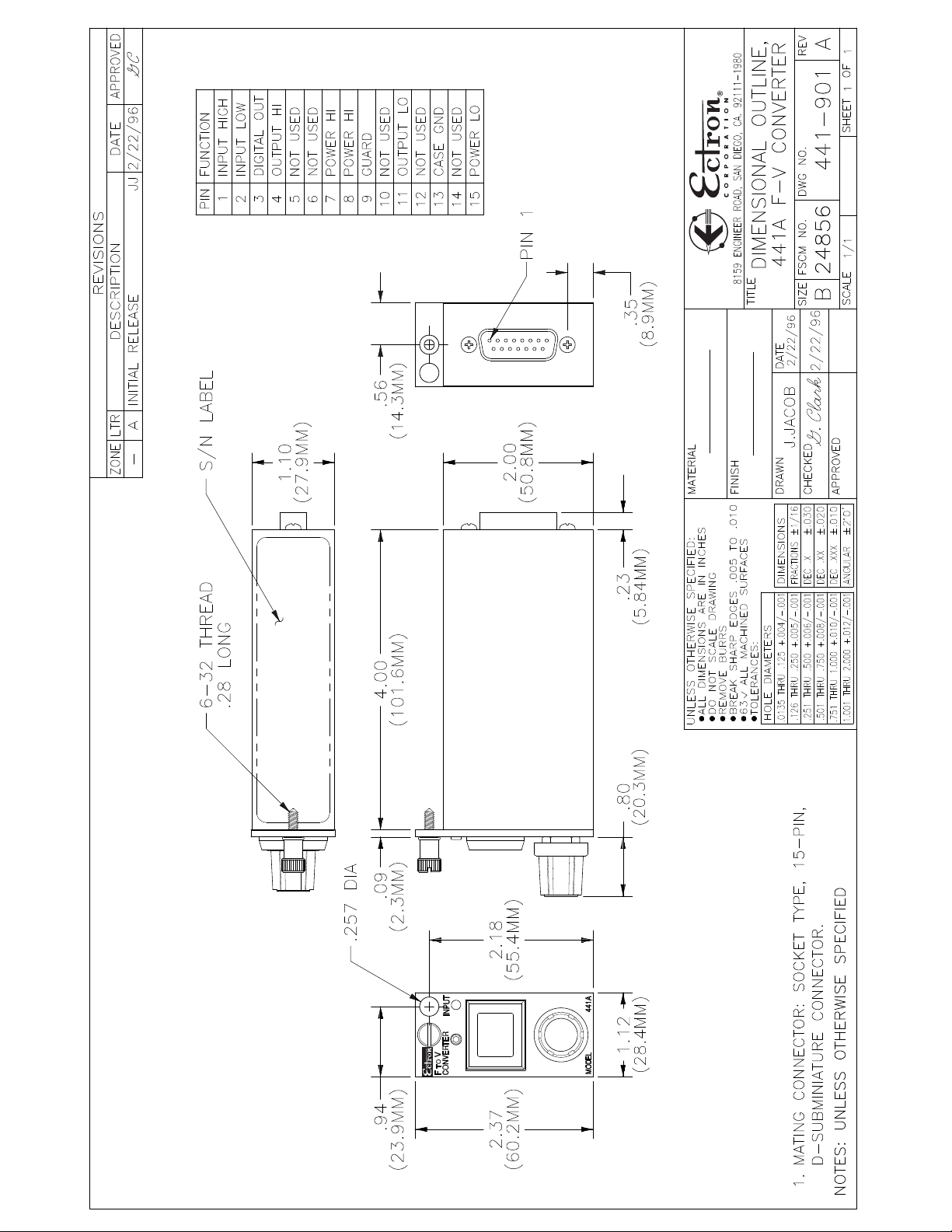


D
C
B
A
A
REV.DWG. NO.SHEET OF
NOTED
APPROVEDDATEDESCRIPTION
REV.
K.C.
3.60
R
SCALE
7/12/05
408-900
JJ
FRONT VIEWTOP VIEW
DWG. NO.
SCALE: 1/2
2.10
REVISIONS
8159 ENGINEER ROAD, SAN DIEGO, CA. 92111-1980
TITLE
DIMENSIONAL OUTLINE, 408-1
SINGLE CHANNEL MOUNT
1 1 408-900 A
MATERIAL
FINISH
1234
2 1
ZONE REV
C
DWG. SIZE
24856
FED. SUPP. CODE NO.
APPROVED
DATES
7/12/05
K.C.
SIGNATURES
DESIGN
EDGES &
ALL SHARP
.030
1/16
±±±±±
.X
FRACTIONS
DEC
DEBURR
COMPLETE
.020
.010
2°0'
.XX
DEC
RMS 125
.XXX
DEC
ANGULAR
SIMILAR TO
FINAL ASSY
NONE
NONE
7/12/05
J. JACOB
DRAWN
CHECKED
REMOVE
RECOMMENDED MULTI-CHANNEL SPACING
RELEASEDA
ALL DIMENSIONS ARE IN INCHES
UNLESS OTHERWISE SPECIFIED
—
—DO NOT SCALE DRAWING
—TOLERANCES:
3.522.75
2.06
.56
1.00
FRONT VIEW
ALL MTG.
HOLES ARE
.196 DIA.
TOP RIGHT SIDE LEFT SIDEREAR BOTTOM
3
5.98
3.002.13
TOP VIEW
3.00
2.13
SIDE VIEW
SCALE: 1/1
SCALE: 1/2
BRACKET DETAIL
OPTIONAL DIN RAIL
MOUNTING BRACKET
TYPICAL MOUNTING POSITIONS USING #10 HARDWARE
4
D
1.035
C
2.75
.385
REAR VIEW
B
A

 Loading...