

.
.n
Y
EPA
POUUllON
PREVENTER
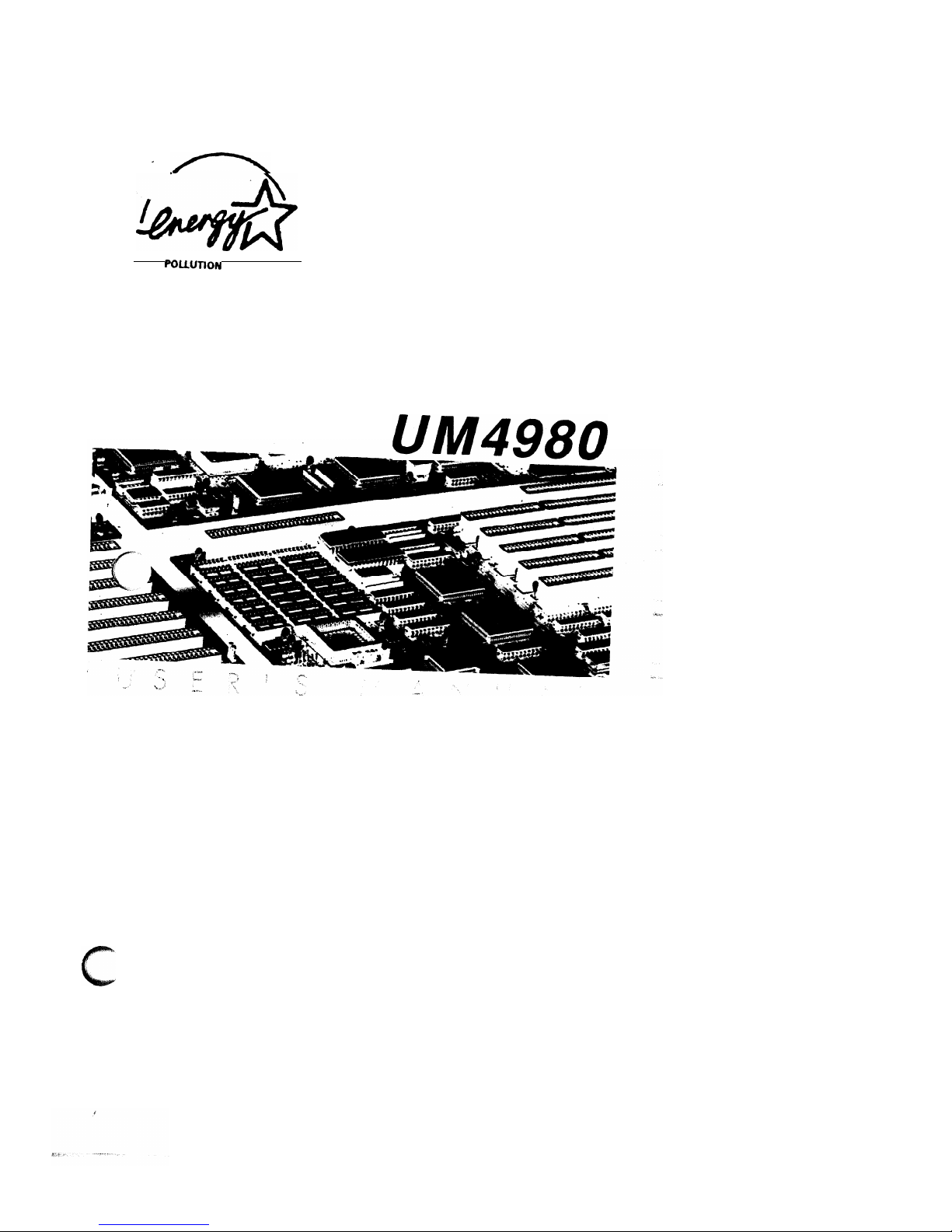
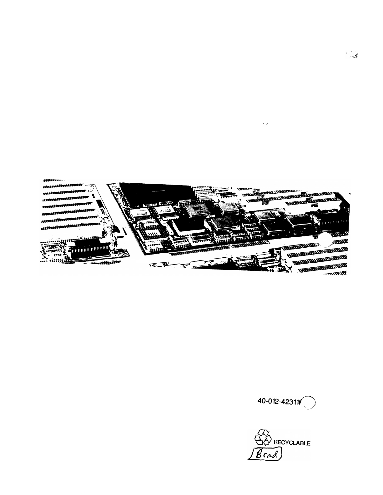
UM4980
-
-._-
40-012-42311/1,
Version 1.1 ’ -
,’
Made in Taiwan

UM4980
User’s Manual

Trademarks
All brand and product names used in this manual may be trademarks or registered trademarks of their respective companies.

W
Table of Contents
Introduction
General Specifications
. . . . . . . . . . . . . . . . . . . . . . . . . . . . . . . . . . . . . . . . . . . . . . . . . . . . . .
1
System Memory
Memory Configurations
. . . . . . . . . . . . . . ..*...................................
3
Cache Memory Subsystem
. . . . . . . . . . . . . . . . . . . . . . . . . . . . . . . . . . . . . . . . . . . . . . . . .
5
Jumper Settings and Connectors
Setting the Jumpers
. . . . . . . . . . . . . . . . . . . . . . . . . . . . . . . . . . . . . . . . . . . . . . . . . . . . . . . . . .
6
Connectors
. . . . . . . . . . . . . . . . . . . . . . . . . . . . . . . . . . . . . . . . . . . . . . . . . . . . . . . . . . . . . . . . . . . .
9
Board Layout
. . . . . . . . . . . . . . . . . . . . . . . . . . . . . ..*.................................
10
Graphic Descriptions of Jumper Settings
. . . . . . . . . . . . . . . . . . . . . . . . . . . . . . . .
11
Built-in BIOS Setup Program
Setup Program
. . . . . . . . . . . . . . . . . . . . . . . . . . . . . . . . . . . . . . . . . . . . . . . . . . . . . . . . . . . . . . . .
23
System Setup
. . . . . . . . . . . . . . . . . . . . . . . . . . . . . . . . . . . . . . . . . . . . . . . . . . . . . . . . . . . . . . . . .
25
Fixed Disk Setup
. . . . . . . . . . . . . . . . . . . . . . . . . . . . . . . . . . . . . . . . . . . . . . . . . . . . . . . . . . . . .
26
Advanced System Setup
. . . . . . . . . . . . . . . . . . . . . . . . . . . . . . . . . . . . . . . . . . . . . . . . . . . .
28
Boot Options
. . . . . . . . . . . . . . . . . . . . . . . . . . . . . . . . . . . . . . . . . . . . . . . . . . . . . . . . . . . . . . . . . .
33
Security
. . . . . . . . . . . . . . . . . . . . . . . . . . . . . . . . . . . . . . . . . . . . . . . . . . . . . . . . . ..*............
34
Green PC Features
. . . . . . . . . . . . . . . . . . . . . . . . . . . . . . . . . . . . . . . . . . . . . . . . . . . . . . . . . .
35
Load ROM Default Values
. . . . . . . . . . . . . . . . . . . . . . . . . . . . . . . . . . . . . . . . . . . . . . . . .
38
Load Values from CMOS
. . . . . . . . . . . . . . . . . . . . . . . . . . . . . . . . . . . . . . . . . . . . . ...*.
39
Save Values to CMOS
. . . . . . . . . . . . . . . . . . . . . . . . . . . . . . . . . . . . . . . . . . . . . . . . . . . . . .
40
Quitting Setup
. . . . . . . . . . . . . . . . . . . . . . . . . . . . . . . . . . . . . . . . . . . . . . . . . . . . . . . . . . . . . . . .
41
Appendix A
Setting the System Speed
1 Introduction
The UM4980 is a high performance 80486 VL-Bus mainboard which includes
UM8498F
and
UM8496F
chipsets. It also supports high integration
&
high performance solution.
1 .l General Specifications
Processor:
Chipset:
System BIOS:
Keyboard BIOS:
System Memory:
Cache Memory:
Slots
:
Connectors:
Form Factor:
Intel 80486
SX/SX2, 80487SX,
80486DX/DX2/DX4, P24D
Cyrix Cx486S (M6), Cx486DXIDX2 (M7)
AMD
Am486DX/DX2,
Am486DXL/DXL2
UMC Green CPU
U5S-SUPER
UMC 8498F, UMC 8496F
Phoenix
AMI
KEYII
DRAM = > 72 pins SIMM single or double density
EPRdM=>27C512
12812561512 KB, 1 MB
Seven (7) 16-bit AT slots
One
(I)
8-bit XT slot
Three (3) VL-Bus slots
Standard Power Connector
Hard ware Reset Connector
Ext Speaker Connector
External Battery
Turbo Switch
Suspend/Resume Push Botton
Turbo LED
Keylock Connector, Power LED
Keyboard Connector
4 layers, 2/3 Baby-AT
UM4980
User’s
Manual
Features
l
100% IBM PC/AT compatible
l
Supports Local Bus Access
l
Supports H/W and S/W Turbo Control
l
Provides Fast CPU Reset and Fast Gate 20
l
Built-in direct map write through & write back cache controller
l
Flexible cache memory size
128/256/512
KB/lMB
l
Supports four banks memory up to 64MB
l
Supports double density for bank2 and bank3
l
Supports 64MB addressing space for DMA
l
Seven AT Bus slots including three VESA master slots
l
Performs zero wait burst read for the 486 CPU
l
Programmable DRAM Access wait state O/l
/2
l
One
237/238
ZIF pins CPU socket which supports
486SX/SX2/DX/DX2/DX4, AMD486/M6/M7/P24D/U5
UM4980
User’s Manual
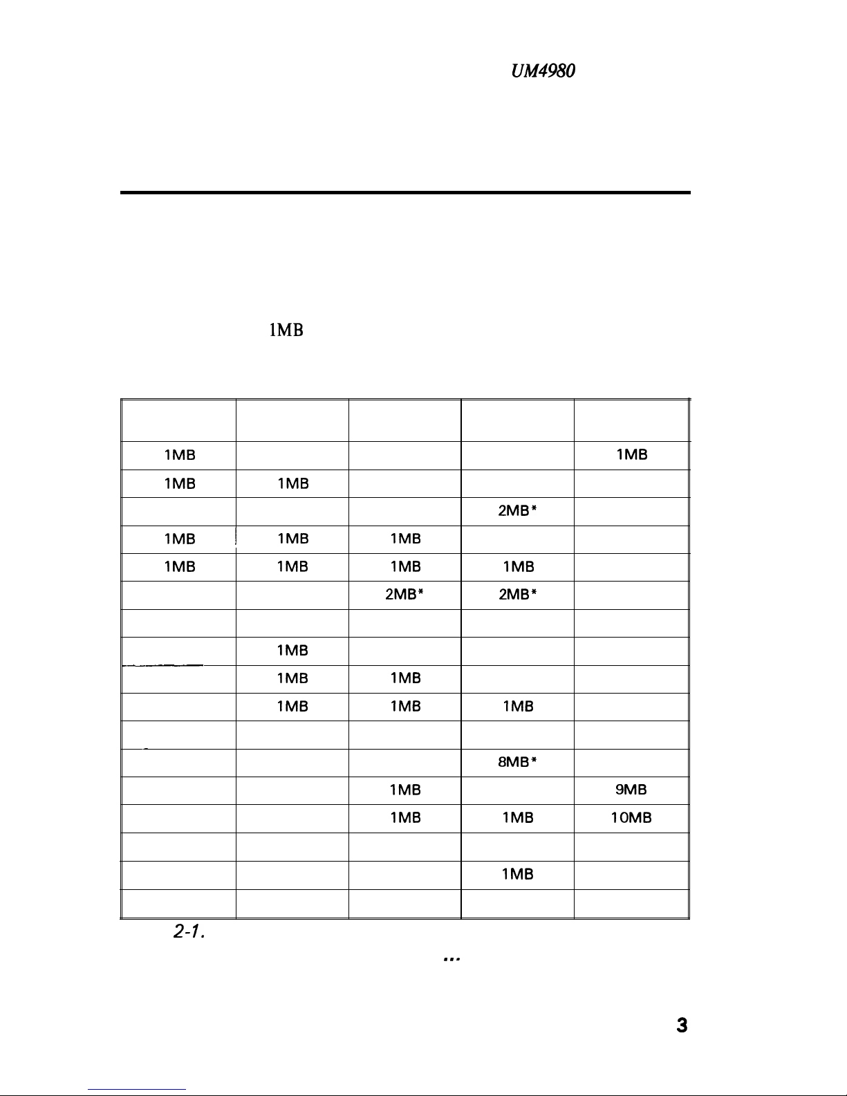
2 System Memory
2.1 Memory
Configurations
The UM4980
provides tremendous flexibility to support a number of different on-board DRAM configurations. The on-board DRAM is installed with
Single-In-Line Memory Module (SIMM). There are four memory banks capable of supporting
1MB
up to 64MB.
The following table lists all the possible DRAM module combinations and
the total memory amount for each option.
SIMM 1
SIMM 2 SIMM 3
SIMM4
Tot
al
Memory Size
IMB
IMB
IMB
IMB
2MB
2MB”
2MB
IMB
,
I
IMB
IMB
3MB
IMB
IMB
IMB IMB
4MB
2MB” 2MB” 4MB
4MB
4MB
4MB
IMB
5MB
--______
4MB
IMB
1MB
6MB
4MB
1MB
IMB
IMB
7MB
4MB
4MB
8MB
8MB”
8MB
4MB
4MB
IMB
9MB
4MB
4MB
IMB
1MB
IOMB
4MB
4MB 4MB 12MB
4MB
4MB 4MB
IMB
13MB
4MB 4MB 4MB
4MB
16MB
Table 2- 1. Memory Bank Configurations and Requirements
Continued..
. . .
3
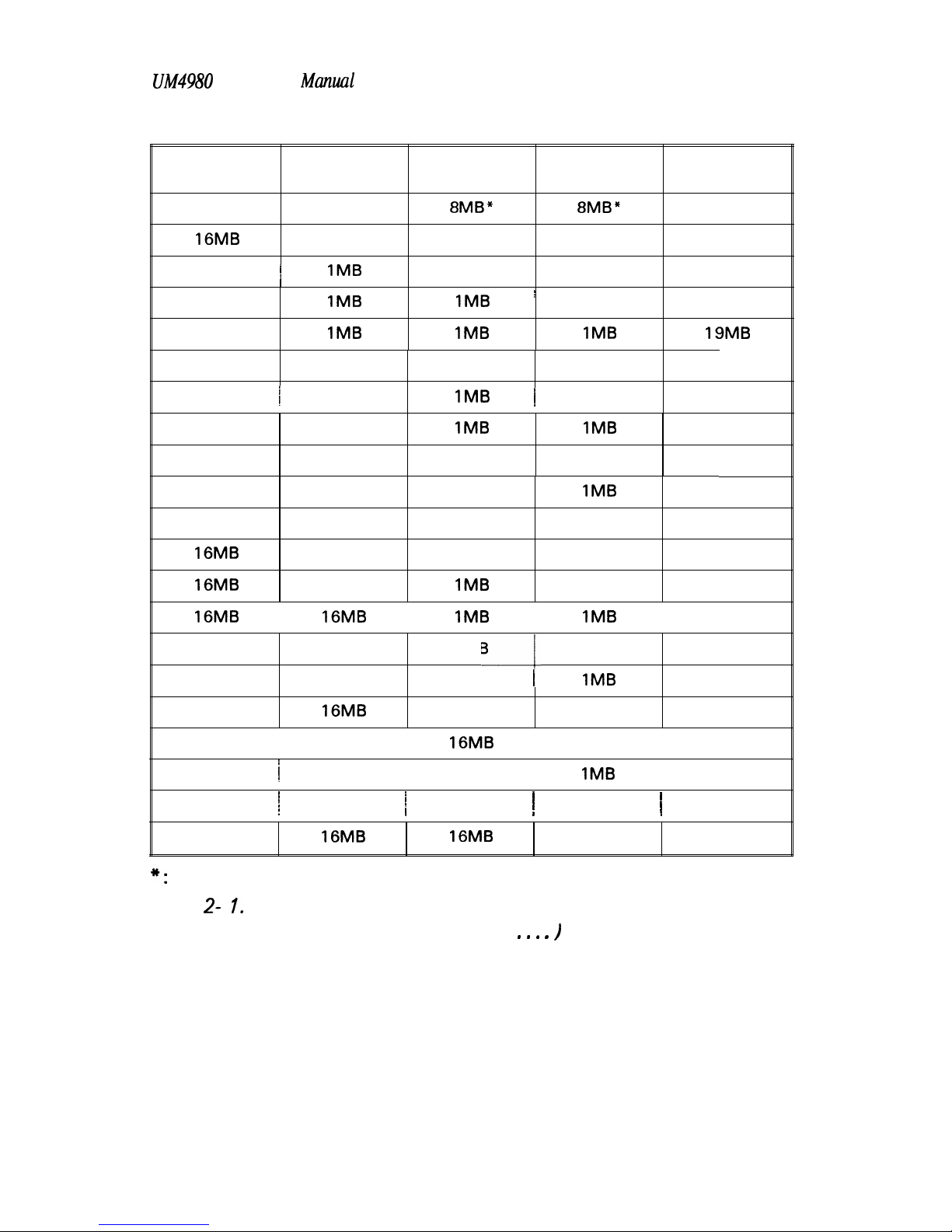
UM4980
User's
Manud
SIMM 1
SIMM 2
SIMM 3 SIMM 4
Total
Memory Size
8MB” 8MB”
16MB
16MB 16MB
16MB
/
1MB
17MB
16MB
1MB
IMB
’
18MB
16MB
1MB
IMB
IMB
19MB
16MB 4MB 20MB
16MB
1
4MB
IMB
1
21MB
16MB 4MB
IMB
IMB
22MB
16MB 4MB 4MB 24MB
16MB 4MB 4MB
IMB
25MB
16MB
4MB
4MB
4MB 28MB
16MB 16MB 32MB
16MB 16MB
IMB
33MB
16MB
I
16MB
I
IMB
I
IMB
I
34MB
16MB 16MB 4MB
/
36MB
16MB 16MB 4MB
1
1MB
37MB
16MB 16MB 4MB
4MB 40MB
16MB
I
16MB
I
16MB
I
I
48MB
16MB
j
16MB
I
16MB
I
IMB
I
49MB
16MB
j
16MB
j
16MB
1
4MB
/
52MB
16MB 16MB 16MB 16MB 64MB
*: It means double density.
Table
2- 1.
Memory Bank Configurations and Requirements
(Continued. . . . .
I
4
UM4980
User’s
Munuul
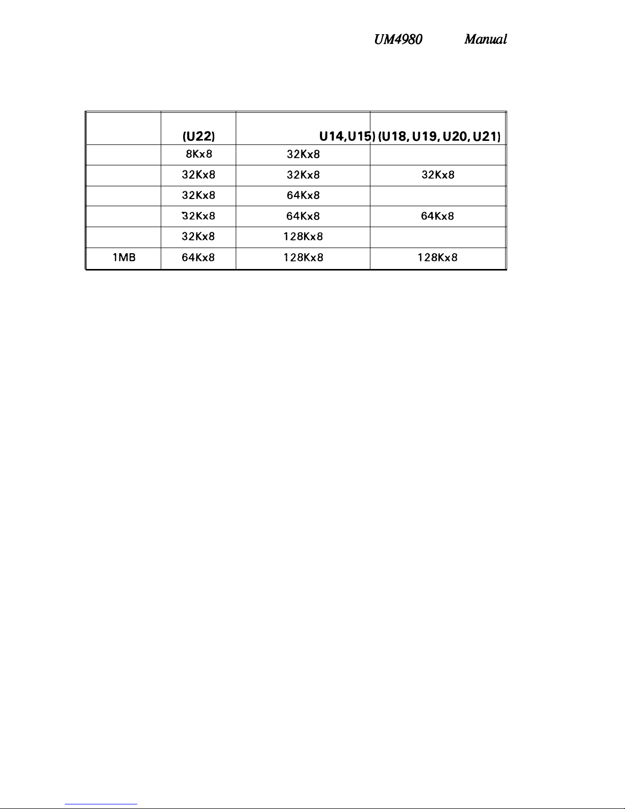
2.2 Cache Memory Configuration
Option
TAG RAM
Cache Bank0
Cache Bank 1
NJ221
(U12, U13,
U14,U15)
(U18, U19, U20, U21)
128K 8Kx8
32Kx8
None
256K
32Kx8 32Kx8
32Kx8
256K
32Kx8 64Kx8
None
512K
32Kx8 64Kx8
64Kx8
512K
32Kx8
128Kx8
None
1MB
64Kx8 128Kx8
128Kx8
Table 2-2. Secondary Cache Memory Configurations
5
UM4980
User's
Manual
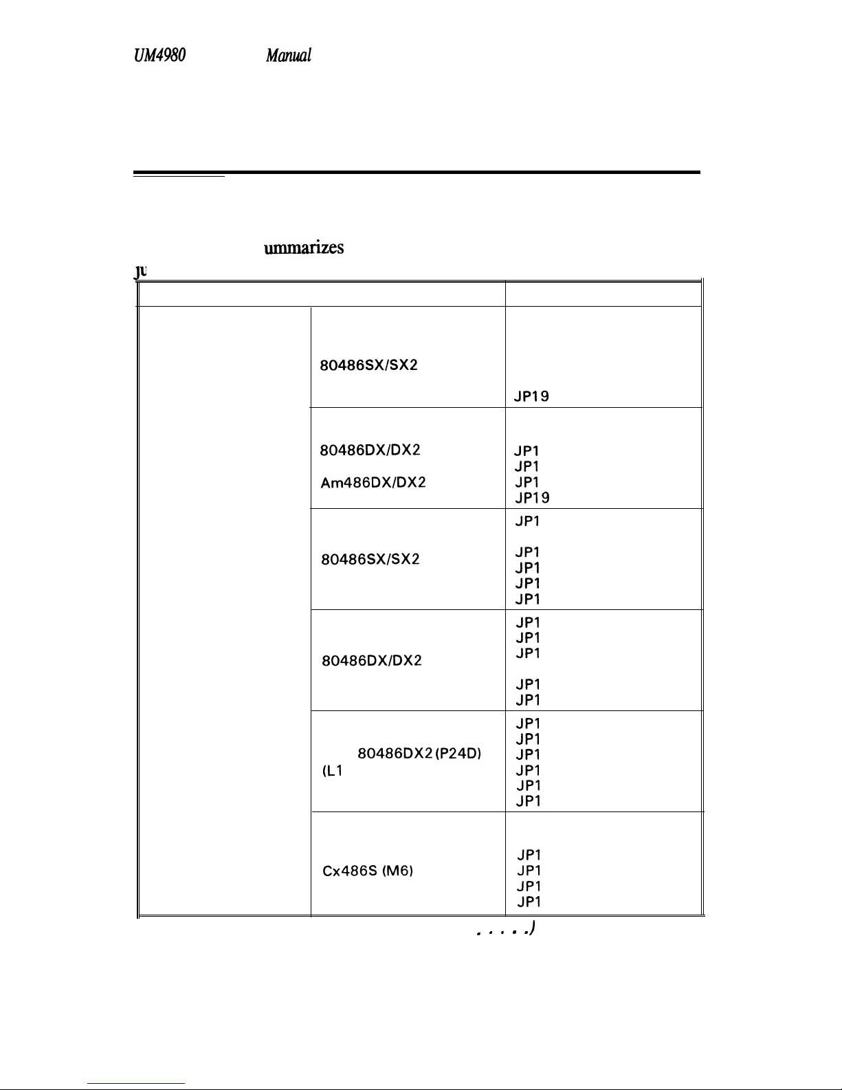
3 Jumper Settings and Connectors
3.1 Setting the Jumpers
The table below s
ummarizes the appropriate functions and settings of each
jumper on the UM4980.
CPU Type
Function
Intel
80486SXISX2
Intel
80486DX/DX2
AMD
Am486DX/DX2
Intel
80486SX/SX2
(SL Enhance)
Intel
80486DX/DX2
(SL Enhance)
Intel
80486DX2 (P24D)
(Ll
Write-Back)
Cyrix
Cx486S (M6)
Jumper Settings
JP14 open
JP15 short 2-3
JP16 open
JP17 open
JP18 short
2-3
JPl9
open
JP14 open
JP15 short l-2, 3-4
JPI
6 short l-2
JPI
7 open
JPI
8 short
2-3
JP19
open
JPI
4 short
1-2, 3-4
JP15 short 2-3
JPI
6 open
JPI
7 short 5-6
JPI
8 short 1-2
JPI
9 short
1-2
JPI
4 short l-2, 3-4
JPI
5 short
l-2, 3-4
JPI
6 short l-2
JP17 short 5-6
JPI
8 short l-2
JPI
9 short 1-2
JPI
4 short
l-2, 3-4
JPI
5 short l-2, 3-4
JPI
6 short l-2
JPI
7 short
3-4, 5-6
JPI
8 short l-2, 4-5
JPI
9 short
l-2, 4-5
JP14 short 2-3, 4-5
JP15 short 2-3
JPI
6 open
JPI
7 short
2-3, 4-5
JPI
8 short l-2,
3-4, 5-6
JPI
9 short l-2,
3-4, 5-6
Table
3-7
.
Jumper Settings (Continued
.
. . .
.
)
6
UM4980
User’s
Manual
CPU Type
Function
cyrix
Cx486DX/DX2
UMC Green CPU
UFiS-Super
AMD
Am486DXL/DXL2
Jumper Settings
JP14 short 2-3
JP15 short l-2, 3-4
JP16 short l-2
JPI
7 short 2-3,
4-5
JPI
8 short 1-2,
3-4, 5-6
JPI
9 short 1-2,
3-4
JP14 open
JP15 short 2-3
JP16 short 3-4
JPI
7 short 1-2
JP18 short 2-3
JPI
9 short 2-3
JPI
4 open
JP15 short l-2, 3-4
JP16 short l-2, 3-4
JPI
7 short l-2
JPI
8 short 2-3
JP19 short 2-3
Intel
804860X4
JP14 short l-2, 3-4
JPI
5 short 1-2,
3-4
JPI
6 short l-2
JPI
7 short 5-6
JPI
8 short 1-2
JP19 short 1-2
Clock Select
25 MHz
33 MHz
40 MHz
50 MHz
JP7 short
JP8 open
JP9 open
JP7 short
JP8 short
JP9 short
JP7 short
JP8 short
JP9 open
JP7 open
JP8 open
JP9 short
JP4 short 1-2
JP5 short l-2
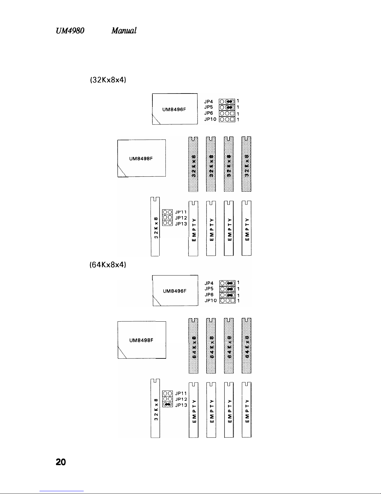
128KB (32Kx8x4)
JP6 open
Cache Memory Settings (one bank)
JPI
0 open
JPll
open
JP12 open
JPI 3open
Table
3-
7.
Jumper Settings (Continued
. . .
,
.)
7
UM4980
User's
Manual
Function
Cache Memory Settings
Local Bus Write Wait
Select
Local Bus Speed
Selec
CPU Voltage
256KB
(64Kx8x4)
[one bank)
256KB
(32Kx8x8)
(two bank)
512KB
(64Kx8x8)
(two bank)
5 12KB
(128x8~4)
(one bank)
II
I
Table 3- I. Jumper Settings (Continued.. . .
.)
1
MB (I
28Kx8x8)
(two bank)
0 Wait State
I
Wait State
<
=
33MHz
> 33MHz
+ 5V (Source from
standard power supply
unit)
Jumper Settings
JP4 short l-2
JP5 short l-2
JP6 short l-2
JPIO
open
JPI I
open
JP12 open
JPI 3 short
JP4 short 2-3
JP5 short 2-3
JP6 open
JPIO
open
JPI
1 open
JPI
2 open
JPI
3 short
JP4 short 2-3
JP5 short 2-3
JP6 short 2-3
JPIO
open
JPI I
short
JP12 open
JPI
3 short
JP4 short l-2
JP5 short 2-3
JP6 short 2-3
JPI
0 short l-2
JPI
1 short
JPI
2 open
JPI
3 short
JP4 short 2-3
JP5 short 2-3
JP6 short 2-3
JPIO
short 2-3
JPI
1 short
JPI
2 short
JPI
3 short
JP26 open
JP26 short
JP25 open
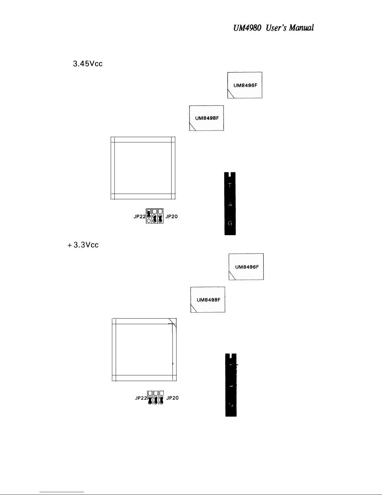
+
3.45V
(Source from on
JP20
short 2-3
board regulator)
JP21 short 2-3
JP22 short l-2
8
VM4980 User’s Manual
Function
I
Jumper Settings
II
CPU Voltage
+
3.3V
(Source from on
board regulator)
JP20
short 2-3
JP21 short 2-3
JP22 short 2-3
Flash ROM
only when programming
a + 5V flash ROM
JPl
short 3-2
only when programming
a +
12V
flash ROM
JPI
short 2-3
Normal EPROM
JPl
open
II
Note:
JP24: Opens for
DX4
Internal CLK 3X
Shorts for DX4 Internal CL K 2X
(2-3).
JP3:
Opens for external keyboard control
Shorts for in
ternal
keyboard control.
3.2 Connectors
There are several connectors located on the
UM4980.
They are used to connect with some peripheral devices to enhance the operating performance of
the system. Refer to Figure 3.1 for the positions of all the connectors on the
mainboard. The following table lists the connectors on the
UM4980.
Connector Function
Jl
Power Supply Connector
J2 External Battery Connector
-
J3 Keyboard Connector
J27
Suspend/Resume (Push Botton)
J28 Turbo LED
J29
External Speaker Connector
J30
Hard ware Reset Connector
J31
Turbo Switch
J32
Keyboard Lock/Power LED
Table 3-2. Mainboard Connectors
Note:
You can only push the J27 button to enter suspend/re-
sume modes when the system is in
‘YDLE”
state otherwise the system will halt or your data may be
destroyed.

UM4980
User's
Manual
3.3 Board Layout
Keyboard Connector
VL-Bus
Slots
!L!L
j$j
JP25
JP26
Expansion
Slots
JPl
J32
J31J30
J29
JP9mJP7
JP6
l-----r
CPU
Jl
I
wij--
Power
I L
1
S
I
I
M
2
Connector
B
r’l
I
0
S
r
S
I
M
1
Key(ock
I
Reset
Turbo
\
Turbo \
LED
Suspend
swltdl
Spe8ker
Resume
Figure 3-1.
UM4980
Mainboard Layout
IO

UM4980
User’s Mmuul
3.4
Graphical Descriptions of Jumper Settings
p-G+
signifies ins 1 & 2 are set as “short.”
pB-i!j
means that this jumer is set as “open.”
CPU Type
1.
Intel
80486SX/SX2
CPU installed on-board
\
r
.
CPU
Socket
\
JP15
11

UM4980
User’s Manual
2. Intel
80486DX/DX2/Am486DX/DX2
CPU installed on-board
CPU
Socket
\
LiII
UM8498F
JP15
1
88
01
JPl6; g
JP’4
m
8
4 O
3.
Intel
80486SX/SX2 (SL
Enhance) CPU installed on-board
1 UM8496F 1
JP15
12

UM4980 User'sibzuul
4.
80486 DX/DX2 (SL Enhance) CPU installed on-board
!1
UM8496F
El
UM8498F
r
I-
CPU
Socket
JP15
1
JP14
5. Intel 80486 DX2
(Ll
Write-Back,
P24D)
CPU installed on-board
El
UM8496F
,
JP15
CPU
I
Socket
-
13
UM4980 Vser's_Mmual
6. Cyrix Cx
486s
(M6) CPU installed on-board
-
El
UM8496F
1
UM8498F
J
CPU
Socket
JP17
8
7. Cyrix
Cx486DX/DX2
CPU installed on-board
UM8498F
CPU
Socket
JP15
1
JPl
JP17
6
JPl%
14
UM4980 User'sManuul
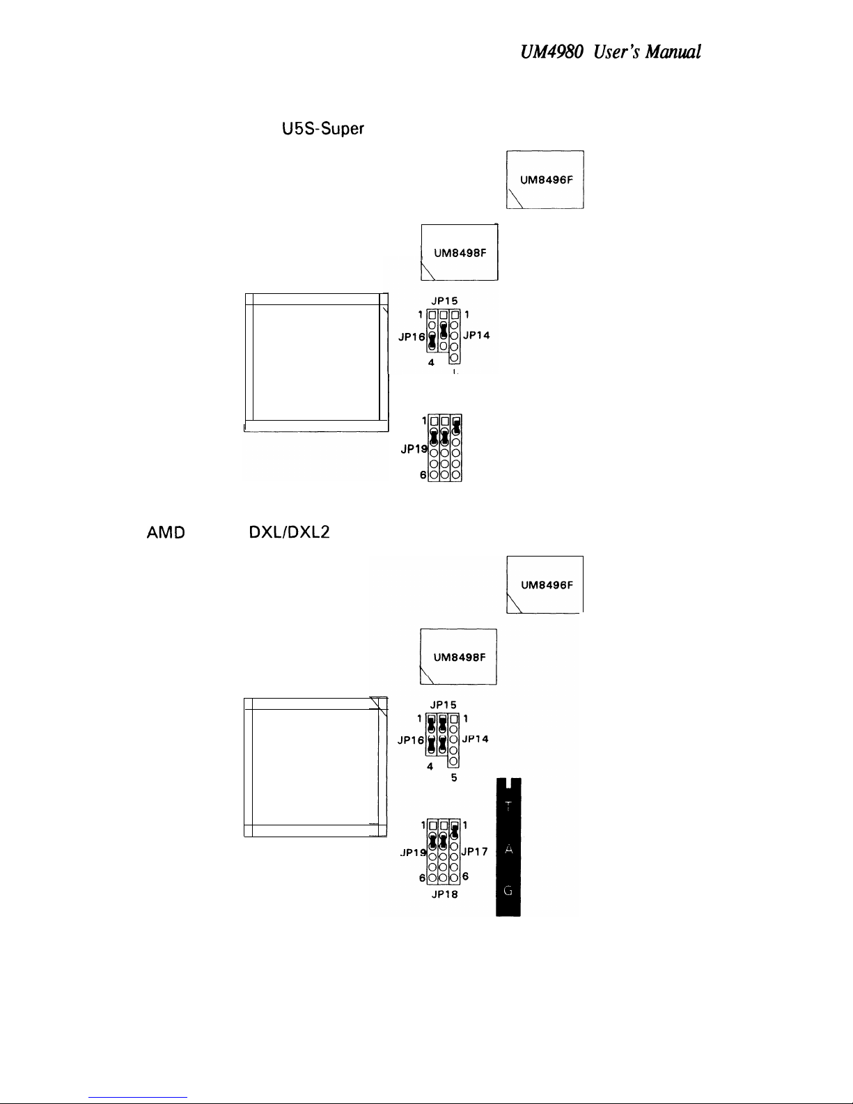
8. UMC Green CPU
U5S-Super
CPU installed on-board
El
UM8496F
1 UM8498F
CPU
Socket
5
1
JPl
JP17
6
JP18
I
9.
AM0
Am486 DXL/DXL2 CPU installed on-board
CPU
Socket
15

UM4980
User's
Manual
10.
80486DX4
CPU installed on-board
CPU
Socket
JP15
1
JP16
1
JP14
1
JPl
JP17
6
JP18
CPU Speed
1. 25MHz CPU Speed
El
UM8496F
JP7
JP8
I
1
UM8498F
h
16
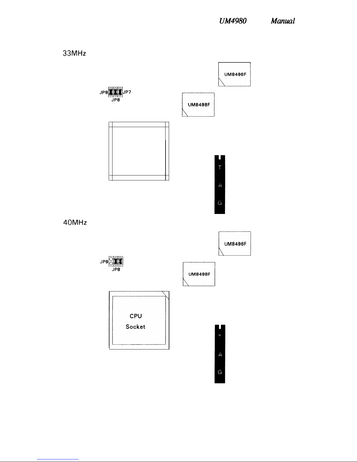
UM4980
User’s
Manual
2. 33MHz CPU Speed
JPQmiJP7
CPU
Socket
,
UM8496F
ll_---J
~
UM8498F
3. 40MHz CPU Speed
El
UM8496F
JP7
17
UM4980
User’s
Manual
4.
5OMHz
CPU Speed
i
UM8496F
CPU
Socket
I
UM8498F
CPU Vcc Source
1. + 5Vcc (source from standard power supply unit)
CPU
Socket
JP20
JP21
h
UM8498F
18
UM4980 User'sManual
2. +
3.45Vcc
(source from on-board regulator)
El
UM8496F
El
UM8498F
CPU
Socket
JP21
3.
+3.3Vcc
(source from on-board
regulator)
CPU
Socket
El
UM8498F
JP22°00
ml
$88
JP20
JP21
19
UM4980
User’s Mmuul
Cache Size Setting
1. 128KB
(32Kx8x4)
Cache Size
w
l-l
2. 256KB
(64Kx8x4)
Cache Size
1
I----
UM8498F
20

UM4980
User’s
Manual
3. 256KB
(32Kx8x8)
Cache Size
I------
UM8498F
4.
512KB
(64Kx8x8)
Cache Size
UM8496F
L
I;
UM8498F
a0
X
.
Y
N
m
u
co
X
Y
e
a
JP4
@@O
1
JP5
Wo
1
w
JP6
000
1
JPlO
000
I
00
X
;
Y
N
m
Lr
a0
X
Y
N
m
00
X
I’
Y
e
co
aD
X
I
Y
N
m
21

UM4980 User’s
Manual
5. 512KB
(128Kx8x4)
Cache Size
l-r
-
U
>
b
4
Lu
-
6. 1 MB
(128Kx8x8)
Cache Memory Settings
h
00
X
1
Y
OD
N
OD
X
I
Y
00
N
-Lr
co
X
Y
a0
N
F
-
22

UM4980
User’s
Manual
4 Built-in BIOS SETUP Program
4.1 SETUP Program
Use the BIOS for
UM4980
to record changes in your hardware and to control its special features. The Setup program uses a number of menus in
which you can specify changes to your hardware and turn the special features to on or off.
To enter the BIOS Setup program, turn on or reboot the system. Press the
<
DEL > key when the system displays the following message:
Press < DEL > to enter Setup. The following screen will then be displayed.
Phanix
Setup -Copiuht 1392-93 Phoenix
Technologies Ltd.
tlain Menu
l
system setup
l Fixed Disk Setup
l
fMuanced system
setup
. Boot Options
l Security
l Green PC Features
Loud Ral Default Values
ILoad
Values from
COWS
Saue Ualues to
CHOS
t1
rlout
Enter Select
ESC Exit
FlO
&we&Exit
Figure 4- 1. SETUP Main Menu
It is highly recommended that you list down all the values of the SETUP
program before making any changes. Doing so will save a lot of time restoring the system back in the event of a configuration memory loss.
Note:
On-screen instructions at the bottom of each
screen
expJain
how to use the program.
n
System Setup
-
allows checking or modification of general configura-
tion information.
23

UM4980
User’s Mmuul
Fixed Disk Setup
-
allows for automatic detection of the hard disk
drive type including the number of cylinders and heads write
pre-com-
pensation
time, read/write head
landmg
zone, and number of sectors
per track.
Advanced System SETUP - sets the various
system
options
for the
user, including the internal/external cache memory
fun&tons,
ISA fea-
tures, video and system shadowing etc..
Boot Options
-
determines the sequence with which the system will
proceed when booting the operating system.
Security
-
rovides
special access for the user to enter the operating
sBstem and
g
etup program, and restricts unauthorized access to the
oppy disk drives.
Green PC Features
-
allows the timer settings for the DOZE,
STANDBY and RESUME modes. It also lists the SMI events by which
the system wakes u
from STANDBY or SUSPEND modes. If the de-
vice is not active,
3
ower Management Function will slow down the
CPU speed and both IDE and monitor will be put into doze, standby,
or suspend mode.
Load ROM Default Values
-
allows for automatic
confi
ation
of
all the above options using-the values in the ROM BIOS ta le.
V
Load Values from CMOS
-
allows for automatic
confi
ation
of all
the above options using the values saved in the CMOS
S
I!ch4
.
Save Values to CMOS - saves the
changes you have made in the
Setup program, then quits and reboots the system.
24
To choose an item from the SETUP main menu, move the cursor to appro-
priate line using the Up < ? > and Down < &
>
arrow
keys and press < En-
&r> .
IBe
screen
wi’L1
display a
wartLirrgmessage
as
sttowa &elow.

UM4980
User’s Manual
4.2
System Setup
?hocnix
setup-
-
Copyright 199t-m ?hoenix Technologies
Ltd.
syotem
setup
sy8ten
Tim:
!&&en
Date:
Uideo
systen:
syutcn
Ilenory
:
Rctenbd knory
cm:sB:591
twe1/19!941
ma /
l&Al
648 KU
3m
Diskette
Drlue CI:
[1.2?!Bl
Diskette blue
B:
mot Inst~lledl
xeybomd:
CIlbSblldl
I
t1
more
Esc
Exit
Paup
Reuioms
u@lue
R Preuioua Conflgwratlon
PyDn Next Ualue
F6
Default Configuration
Figure 4-2. System Setup
System Time
-
includes hour, minutes, seconds but only the values of hour
and minute can be set.
System Date
-
allows manual setting of the electronic calendar on the
main-
board..
Video System
-
specifies the display adapter installed.
System Memory and Extended Memory
-
displays important information
about your system which includes the conventional and extended memory
sizes. They are updated automatically by the Setup program according to
the status detected by the BIOS self-test. This section of the System Setup
screen is for viewing purpose only and manual modifications are notal-
lowed.
Diskette Drives A: and B:
-
specify the capacity and format of the
floppy
drives installed in your system.
Keyboard
-
selects install/Not install for keyboard device setting.
25

UM4980
User’s
Manual
4.3 Fixed Disk Setup
The Fixed Disk Setup provides auto configuration of the hard drive installed
in the system. After pressing the < Enter > key on this item on the main
menu, the screen will display the following screen.
?hoenlx
Setup- Copyright
1992-93 ?hocnix technologi~
Ltd.
l
Fixed Disk 9 Control
l
Fixed
Disk
1 Control
Large Dimk
DOS
Conpatibility:CEnabledl
Tl Houe
Enter Select
CSC exit FlO save & Exit
Figure 4-3. Fixed Disk Setup Screen I
Once the
program detects the type of hard disk 0 and/or 1 installed, it will
display the relative information such as the type, cylinders, heads, write
pre-
compensation, landing zone, and number of sectors per track.
Phoenix Setup-
CopyriDW
1992-93 Phoenix
technoloqies LU.
Fixed
Disk
8
Control
fhltotgpe ?lxed Disk:
m=:
ClJlinlCr#l:
HfdS:
sectors/tr~ck
:
Landing zone:
write
prcconp:
LWI Node
Control:
IDI eabledl
Tl
nouc
Enter
Select
ESC exit
Figure 4-4. Fixed Disk Setup Screen 2
26

UM4980 User’s Manual
If the program fails to detect the hard disk(s) or the < Enter > key was not
pressed in the
Autotype
Fixed Disk oprion, manual setting of the values is
recommended.
Autotype
Fixed
Disk
-
detects the type of fixed disk 0 and/or 1 installed. If
successful, it fills the remaining fields on this menu.
Type
-
1 to 45 fills in remaining fields with values for predefined disk
drives. “User” allows the user to fill in the remaining fields..
Cylinders
-
specifies the number of cylinders of the hard disk drive. The
range of this option is from 1 to 1024.
Heads
-
specifies the number of
read/write
The range of this
option is from
1 to 16.
heads of the
hard
disk drive.
Sectors/Track
-
provides the number of sectors per track defined for the
hard disk drive. The range is from 1 to 64.
Landing Zone
-
refers to the cylinder number where the disk drive heads
(read/write) are positioned to when the disk drive is parked. The range of
this option is from 1 to 1024.
Write Precomp
-
refers the cylinder number, above which, disk drive operations require reduced write current. Also specifies the number of cylinder at which to change the write timing. The available options are from 1 to
1024 and None.
Large Disk DOS Compatibility
-
for Large Hard Disk Compatibility
(Larger than 528MB) issue, you must enable this item except UNIX operating system.
LBA Mode Control -
turns
on or off the hard disk drive’s LBA Mode support. Some HDD support more than 540MB and LBA Mode for data transfer. If your hard disk supports LBA Mode, you should
enable
this
option otherwise
disable(off)
it.
27
UM4980
User’s
Manual
Phoenix Setup-
Copllrlght
1992-93 Phoenix Technologies Ltd.
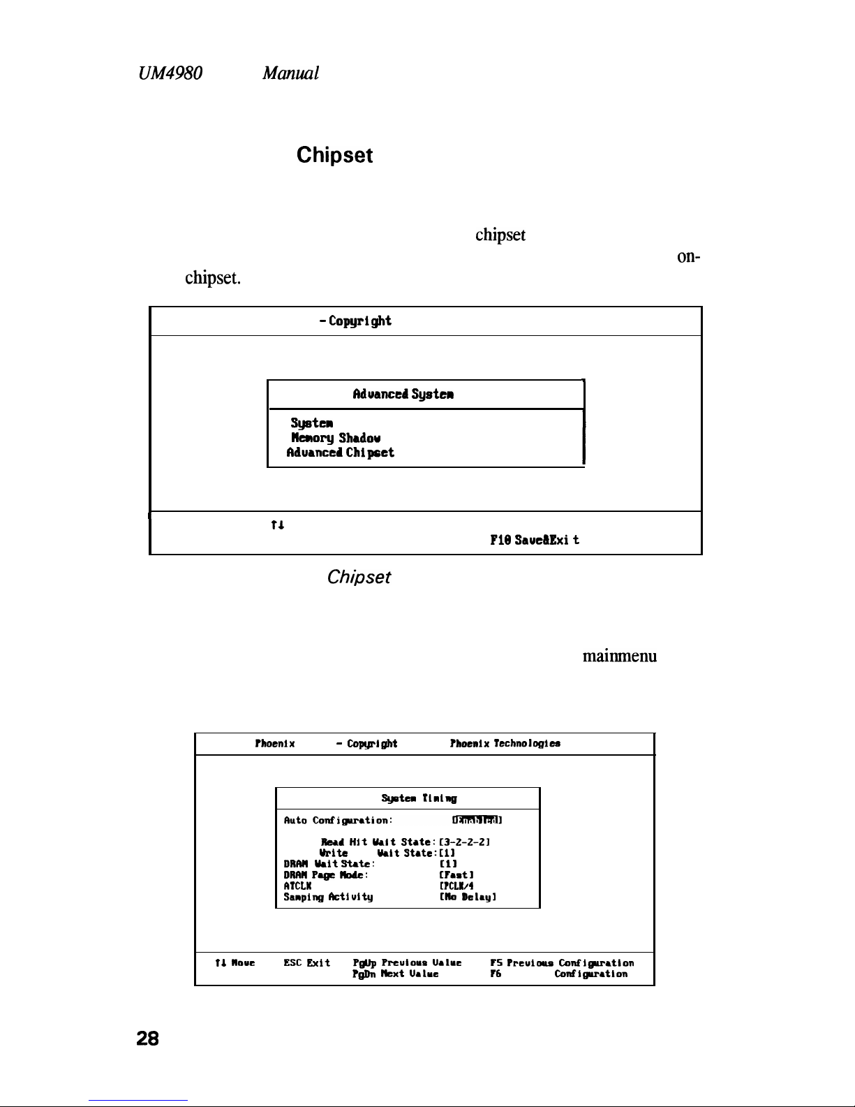
4.4 Advanced
Chipset
SETUP
The Advanced System Setup allows the user to program three main groups
of parameters under the Advanced System Setup namely the System Timing, the Memory Shadow, and the Advanced
chipset
Control. This BIOS
Setup parameter is designed for programmers who wish to fine tune the
on-
board
chipset.
(Iduanced System
Setup
.
l Systen lining
.
Emory Shadou
.
fiduanccd
Chipset Control
I
t1
noue Enter Select
ESC Exit
Pi@ SautIkExi
t
Figure 4-5. Advanced
Cbipset
SETUP Screen
System Timing
Selecting System Timing from the Advanced System Setup
mainmenu
displays the following screen. The actual features displayed depend on the capabilities of your system’s hardware.
?hoenlx
Setup -Copgrlght
1992-93
?haenix
technologies
Ltd.
syaten
Tlnlllg
Cache
Kead Hit Wit State: C3-2-2-21
Cache
Urite
Hit
Wit State:tll
DRfWl
Wit
State:
[II
DRfM Pw Mde: CPmtl
MCLK
Select:
VCLKA
1
Sanping ktluity
Tine:
tllo Del&y1
11
noue
ESC
Exit
P@Jp Prculous blue
PS Preuious Configrshtion
PQDn Ilcxt Ualue
P6
Default
Conf~guratlon
Figure 4-6. System Timing Screen
20

UM4980 User'sManual
Auto Configuration
-
Disabling this option allows the values for the other
parameters to be changed. Enabling it will restrict you from making any
changes.
Cache
ReadHit
Wait State
-
determines the number of cycle times to
be inserted when CPU reads data to cache. The setting depends on the
speed of the CPU and SRAM. If the CPU is of high speed, the time re-
quired by SRAM to process data will need an extension, with the excep-
tion of some
SRAMs
that are fast enough to catch up with the speed of
the CPU. The available options are:
. 3-2-2-2
l 3-l-l-l
l 2-l-l-l
Cache Write Hit Wait State
-
setting of this parameter makes no difference from that of the SRAM Read. This option sets the number of
wait states to be added on writes to cache memory. Fewer wait states
are recommended to improve the system performance. Check the CPU
speed and SRAM before changing the default value. The available options are listed below.
l ows
l
IWS
l 2ws
DRAM Wait State
-
determines the number of wait states to be inserted when the CPU reads data into the local DRAM. Fewer wait
states are recommended to improve the system performance. The following are the available options.
l ows
l 2ws
l
IWS
DRAM Page Mode
-
determines the number of wait states to be inserted when the CPU writes data into the local DRAM. Fewer wait
states are recommended to improve the system performance. The following are the available options.
l Normal
l Fast
29

UM4980
User’s
Manual
AT Bus
Clock Select
-
specifies the speed of the AT Bus clock of the
system. The available options are:
.
PCLK/2
l
PCLK/3
l
PCLK/4
.
PCLK/5
l
PCLK/G
l
PCLK/8
Sampling Activity Time
-
selects the delay time when the
chipset
moni-
tors and samples SMI. The available options are:
l No Delay
l Delay 1 T
Memory Shadow
Select Memory Shadow from the Advanced System Setup main menu displays the following screen. The actual features displayed depend on the capabilities of your system’s hardware.
Phoenix
setrp -
copgri*t
lsvz-¶3
Phomlx rechn01ogia
Ltd.
sbdou
kaory kgIoma
ewe -
cwr:
CDlsabldl
cc08 -
ccl?:
CDlssbldl
wee -
b3R:
tDlsabldl
M08 - D7R:
tDlsabldl
Ime - Inn:
CDLsabldl
DC88 -
DW?:
[Dlsabldl
11
lloue
Esc
exit
r&lp
?rcuiouD
Ualue
15
?nuious
Confifptration
?*n
lbxt
Ualue
P6
Ddamlt
Configuutlon
I
Figure 4-7. Memory Shadow Screen
System shadow
-
allows shadowing of the system BIOS and improves the
system performance. This option is always set as Enabled.
Video shadow
-
sets the mode of the system’s video BIOS shadowing
mode. The available options are:
n Enabled (default)
n
Disabled
30
U.4980
User’s Manual
Shadow Memory Regions
-
shadows the option ROM located in the speci-
fied blocks of memory, and can improve the system performance.
Note:
Some option ROMs do not work properly when
shad-
owed.
Advanced
Chipset
Control
Selecting Advanced
Chipset
Control from the Advanced System Setup main
menu displays the following screen. Technicians use this menu when changing values in the
chipset
register and optimizing the system’s performance.
Phoenix Setup - Copyright
19%+93
Phoenix Technologies Ltd.
Ad
uanced Ch
i pset
Contra
I
Internal cache f
taturc:
d!mmmm
External cache:
[Enabled1
External cache feature:
Write through 1
DM Parity check:
[Disabled]
DlWl
Refresh
Method:
MS only1
Signal
GA208
select:
Khipsctl
Signal RC select: Khipsetl
Local
IDaady
lklay Setting:
liTI
CPU
ADSu
Delay:
Ctbnel
IA
Recovery Time Select
:
c5.31
.
I
11 ebue
ESC Exit
PgUp Preuious Ualue
FS
Prcuiws Configuration
PgDn
Wext Ualue
F6
Default Configuration
Figure 4-8. Advanced
Chipset
Control Screen
Note:
The contents of this menu depends on the
chipset
in-
stalled on your mainboard, and
chipsets
vary widely.
Consult your dealer or the < FI > help screens before
changing the items on this menu. Incorrect settings
can cause your system to malfunction.
Internal cache feature
-
sets the internal code/data memory of the CPU to
either
White
back or
White
through (default)
External cache - sets the function of the second level cache on-board.
If
En-
abled (default), the settings of the following options can be set. Disabling
this option will deem the following options useless.
External cache feature
-
sets the external secondary cache memory to
either
White
back (default) or
White
through.
31
U.4980
User’s
Manual
DRAM Parity Check - During a local memory read cycle, the
UM8498F
not
only
monitors bus steering, but also checks the parity bit for each data
byte from DRAM to ensure that the
correct.data
is read. The available op-
tions are:
n
Enabled
n Disabled (default)
DRAM Refresh Method - specifies the timing pulse width where the row
address strobe (RAS) will be on the falling edge and followed by the column address strobe signal (CAS). The available options are:
n
RAS only (default)
n CAS before RAS
Signal
GA20#
Select - sets the method of select Signal
GA20#
from Key-
board Controller or
UM8498F Chipset
Emulate. The available options are
listed below.
n Chipset (default)
q
Keyboard
Signale
RC select - sets the method of select Signal RC. The available op-
tions are:
n Chipset (default)
n Keyboard
Local Ready Delay Setting - sets the
delay time of Local Ready Signal.
The available options are:
n
IT (default)
n
2T
n
3T
n None
CPU
ADS#
Delay - The
available options are:
n
None (default)
n
IT
I/O
recovery Time Select - specifies the I/O command recovery time ex-
cept for some add-on cards. The available options
are:
n
0,0/1,1/2,2/3,3/5,5/7,7/9,9/12,12
m 5,3
(default)
n
7,3/9,3/l 2,3
32
UM4980
User’s
Manual
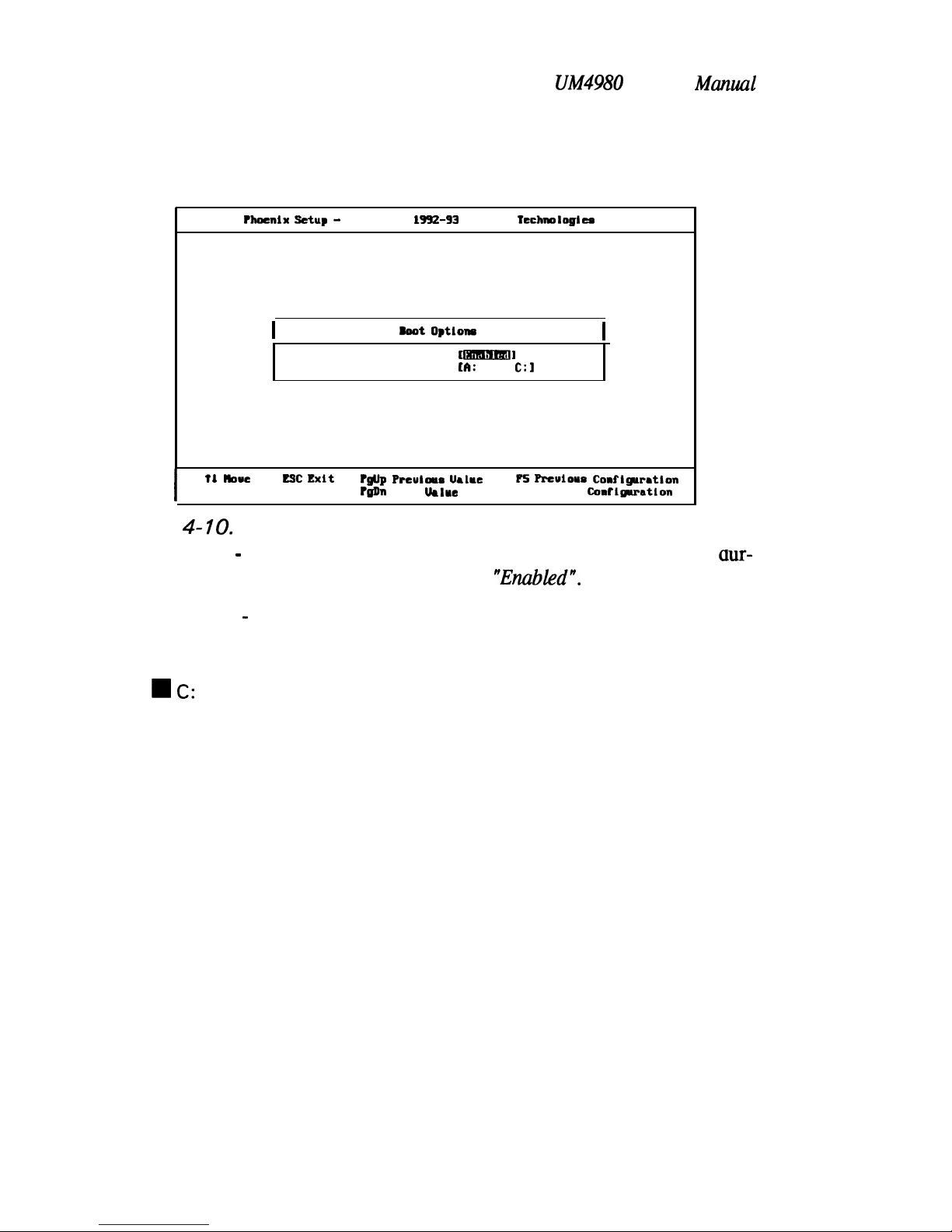
4.5 Boot Options
Phoenix Setup -Copyrlght 1992-93 Phoenix
Tcchnologles
Ltd.
I
hot Optlonu
I
Floppy check::
t-1
Boot sequence:
tcI:
then
C:l
I
Tl but
Esc
Exit
?#Jp
Preuloua
Ualrc
PS Prcuious Conflgiratlon
?gDn
Next Ualue P6 Default
Corflguration
Figure 4-
IO.
Boot Options Screen
Floppy check - allows the system to search and verify the floppy drives
aur-
ing boot. The default value for this option is
"Enubkd".
Boot sequence - sets the sequence from where the BIOS will attempt to
load the operating system. The options are:
n
C: then A:
W
C:
only
n
A: then C: (default)
33

UM4980
User’s
Manual
4.6 Security
I
Phoenix
SGtup- Copyright
1992-93
Phoenix Technologies Ltd.
Security
Supcruisor Passmrd
is
Disabled
I
I
Passuord
on boot:
CDl=bledl
I
Diskette access:
cSuperuisar
1
I
t4
noue
Enter
StAhange
Passuord
ESC Exlt
Figure 4- I
I.
Security Screen
P5
Preuicms ConfIguratIon
P6
Default Conflguratlon
Supervisor Password is
-
shows whether the supervisor password is en-
abled
or
disabled
(default).
User Password is
-
shows whether the user password is enabled or disabled
(default).
Set Supervisor Password
-
requires a password when entering Setup, the
passwords are not case sensitive. Pressing the < Enter > key will display a
message requiring for the supervisor password which can be up to seven alphanumeric characters. This option also gives full access to the Setup
menus.
Set User Password
-
Pressing the < Enter > key will display a message requiring for the user password which can be up to seven alphanumeric characters. This option also gives restricted access to the Setup menus and
requires the setting of the Supervisor Password first.
Password on boot
-
determines whether the password is required on boot.
The option needs the setting of the Supervisor Password. If Supervisor Password is set and this option is
disabkd
(default). BIOS assumes that the user
is booting.
Diskette access
-
restricts the use of floppy drives only to the supervisor
when set as Supervisor (default). Also, choosing Supervisor for this option
will require the setting of the Supervisor Password. Setting is as User allows access to the floppy drives at any time.
34
UM4980
User’s
Mlwwul
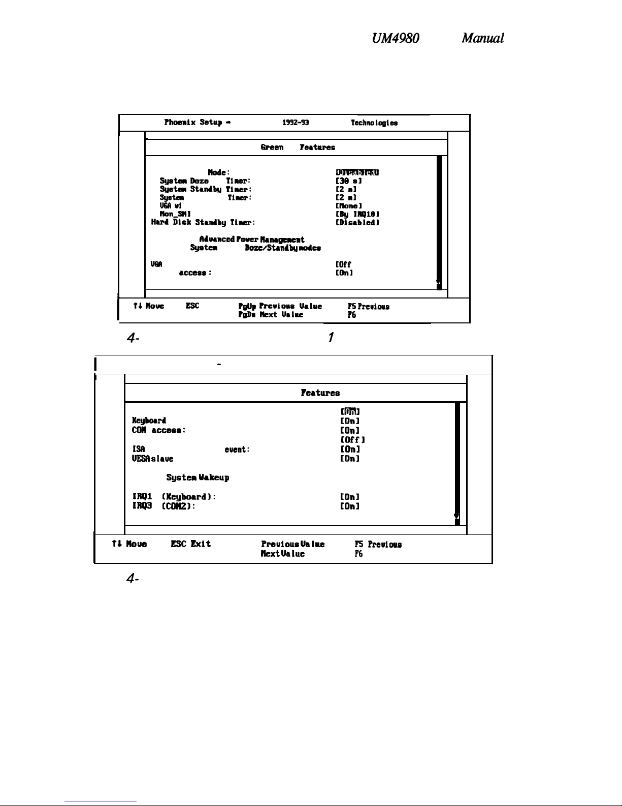
4.7 Green PC Features
Pboenlx
setup -
Copyright
1992-93
Phoenix
Technologies
Ltd.
6reen
PC
Featllrec
Power Swing
Node:
cm
-
‘.
1
systen
Doze
Ti ner :
130
di
sythen standby Timber:
12 nl
systar
suspend
Tiner:
Et nl
U6fi ui
th
Power Down feature:
UtOlM91
llon_SlI
CPU wpport:
CBy Illq11Bl
Hurl Dltk Standby Ilner:
~Dlcablsdl
Clduanccd ?oucr
Wanagcnent Setup
Syatcn
enters
bozc/Standby noks
by:
Um
access:
Floppy
access
:
[Off
I
COnl
v
I
14
Hove
ESC
Exit
?gUp Rcuiows UaLuc
FS Preuiour,
Configuration
PnDn kxt Value
P6
Default
Configuration
Figure 4- 12. Green PC Features Screen
I
I
Phoenix Setup -Copyright 1992-93 Phoenix
Technologies
Ltd.
Green
PC
Peaturcs
Hard Disk access:
mEi1
Heyboard
access:
COnl
COW access:
[On1
LPI access:
[Off1
Is(I
Master access
went:
[On1
UESA slrue
access:
[On1
Systen
Uakeup
fror Suspend nodes by:
IRQl Ueyborrdl:
IRQ3 ccon21:
[On1
[On1
v
l&
moue
ESC
Exit
PgUp
Preuious
Ualwe
FS
Preulow
Configuration
PgDn
Next
Ualut
F6
Default Configuration
Figure 4- 13. Green PC Features Screen2
35

UM4980
User’s
Munuul
Phoenix Setup- Copyright 1932-93 Phoenix Technologies Ltd.
Green PC
Peatqres
IRQ4 CCbHl):
mm
A
IRQS Wilt. printerl:
[Off1
IRQ7 [Printer):
[On1
IRQ3
[Off1
IRQl0
COffl
IRQll
[On1
IRQlZ CPS&
rouse):
[Off I
IRQIS :
[On1
ISCI ?laster/D?W: [On1
TL moue
ESC
Exit
PgUp Preuious Ualue
'
P5
Preuious Configuration
PgDn Next
Ualue
P6
Default Configuration
Figure 4- 14. Green PC Features Screen3
Power Saving Mode - enables or disables (default) the power saving mode
feature of the
chipset.
Once enabled, the values of the following options can
be set.
System Doze Timer - sets the time interval after system inactivity
when the system enters DOZE mode. The available options are:
l 30 s (default)
l 1
I21418
m
l Disabled
System Standby Timer - sets
the
time interval after system inactivity
when the system events enters STANDBY mode. The options are:
l 2 m (default)
l
4/8/l 6/32/64/l
2812561512 m
l Disabled
System Suspend Timer - sets the time interval after system inactivity
when the system enters SUSPEND mode. The available options are:
l 2 m (default)
l
4/8/l 6/32/64/l
2812561512 m
l Disabled
VGA with Power Down features
-
sets the
method by which the VGA
chip enters SLEEP mode. The options are:
l None (default)
l Standard
l VESA DPMS
36

UM4980
User's
Manual
Non-SMI CPU Support - selects the interrupt request signal to replace
System Management Interrupt (SMI) events when the CPU does not
support SMI. The options are:
.
ByIRQ15
l By IRQ IO (default)
Hard Disk Standby Timer - sets the time interval after hard disk inac-
tivity when the system events enter STANDBY mode. The options are:
l Disabled (default)
l 1
m,2mto15
Advance Power Management Setup
System enters Doze/Standby modes by
-
The
menu also lists the System Management Interrupt (SMI) events by which the system wakes up
from
Doze or SUSPEND modes. Switch the following parameters to on
or off:
0
0
0
0
a
0
0
0
VGA access
Floppy access
Hard Disk access
Keyboard access
COM access
LPT access
ISA Master access
VESA Slave access
System Wakeup from Suspend modes by
-
The
menu lists the SMI
events by which the system wakes up from SUSPEND mode. Switch
the following parameters to on or off.
l IRQI (keyboard)
.
IRQ3 (COM2)
l
IRQ4 (COMI)
l
IRQ5 (Alt.
Printer)
l
IRQ7
(Printer)
l
IRQ9
. IRQlO
.
IRQII
l IRQ12
(PS/2,
mouse)
.
lRQl5
l ISA Master/DMA

UM4980
User’s
Manual
4.8 Load ROM Default Values
If, during
bootup,
the BIOS program detects a problem in the integrity of
the CMOS, it will display a message asking you to either press the
<DEL> key to run Setup or the
<
Fl
> key to resume booting. This probably means that the CMOS values have been corrupted or modified incorrectly, perhaps by an application program that changes data stored in
CMOS.
Press the
<
Fl
>
key to resume the boot or <DEL> to run Setup
with
the
ROM default values already loaded in the menus. You can make other
changes before saving the values to CMOS.
Phoenix Setup- Copyright 1992-93 Phoenix Technologies Ltd.
Main
Hem
l
System Setup
Load Ualues
fron CMOS
Saue
Ualues to
C?lOS
b
figure 4-
15.
Load ROM Default Values Screen
38

Uhf4980
User’s
Manuul
4.9
Load Values from CMOS
If, during a Setup session, you change your mind about your selections and
have not yet saved the values to CMOS, you can restore the values you previously saved to CMOS.
Select Load Values
from
CMOS on the Main Menu and the program will
display the following screen.
Phoenix Setup -Copyright
1932-93
Phoenix Technologies Ltd.
Main
Henu
l
systca
setup
Load
Ualues fron CMOS
Saue Ualucs
to
CMOS
Figure 4- 16. Load Values from CMOS Screen
39

UM4980
User's
Manual
4.10 Save Values to CMOS
After making your selections on the
SEtup
menus, always select Save Values to CMOS in order to make them operative. Unlike standard RAM memory, CMOS RAM is sustained by an on-board battery and stays on after you
turn your system off.
After you save your selections, the program will display the following
screen.
Phoenix Setup
-
Copyright
1992-93
Phoenix Technologies Ltd.
llain llenu
Load
Ualucs
fron CMOS
Saue
Ualues
to
CMOS
Figure 4-17. Save Values to CMOS Screen
If you attempt to exit without saving, the program will ask you if you would
like to save the changes made before exiting.
During
bootup,
BIOS for the
chipset
attempts tom load the values you saved
in the CMOS RAM. If the values saved in the CMOS cause the system boot
to fail, reboot and press the < DEL > key to enter Setup. In Setup, you may
load the ROM default value (as described in the section 4.8) or try to
change the values that caused the boot to fail.

UM4980
User’s Manuul
4.11 Quitting Setup
After making all modifications in the Setup program, go to the option “Save
Values to CMOS’ then press the < Enter > key or simply press the
< FlO
> key. The screen will then display a message asking you whether
you would like to save and exit or not.
Use the arrow keys or press < Y > for Yes then the < Enter > key to save
your settings before exiting. Press < N > for No then the < Enter > key to
exit without saving.
If you made changes to the CMOS values and then press the <ESC > key,
the program will prompt you whether you would like to Quit without saving
or not.
Press < Y > for Yes then the C Enter > key to quit without saving, or press
<
N > then the < Enter > key to save your settings first before exiting Setup.
Appendix A
Setting the System Speed
n
High Speed
m
Low Speed
41
 Loading...