

Page 1

Preface
Copyright
This publication, including all photographs, illus trations and software, is protected under international copyright laws, with al l ri ghts reserved. Neither this manual, nor any
of the material cont ai ned herei n, may be reproduced without written consent of the author.
Version 3.2a
Disclaimer
The information in this document is subject to change without notice. The manuf acturer makes no representat i ons or warranties with respect to the cont ent s hereof and
specifically disclaims any implied warranties of merchantability or fitness for any particular purpose. The manuf acturer reserves the right to revise this publication and to
make changes from time to time in t he content hereof without obligation of t he manufacturer to notify any person of such revision or changes.
Trademark Recognition
Microsoft, MS-DOS and Windows are registered trademarks of Microsoft Corp.
MMX, Pentium, Pentium-II, Pentium-III, Celeron are registered trademarks of Intel
Corporation.
Other product names used in this manual are the properties of their respective owners
and are acknowledged.
Federal Communications Commission (FCC)
This equipment has been tes ted and found to comply with the limits for a Class B digi tal device, pursuant to P art 15 of the FCC Rules. These limi ts are designed to provide
reasonable protection against harmful interference in a resi dent i al i nstallation. This
equipment generates, uses, and can radiate radio frequency energy and, if not installed and used in accordanc e with the instructions, may cause harmful interference
to radio communicati ons. However, there is no guarantee that interference will not occur in a particular instal l ation. If this equipm ent does cause harmful interference to
radio or television reception, which can be determined by turning the equipment off
and on, the user is encouraged to try to correct the interference by one or more of the
following measures:
− Reorient or relocate the receiving ant enna.
− Increase the separation between the equipment and the receiver.
− Connect the equipment onto an out l et on a circuit different from that to which
the receiver is connected.
− Consult the dealer or an experienced radio/TV tec hni cian for help.
Shielded interconnect cabl es and a shielded AC power cable must be employed with
this equipment to ens ure compliance with the pertinent RF emission limits governing
this device. Changes or modifications not expressly approved by the system's manufacturer could void the user' s authority to operate the equipm ent .
i
Page 2

Declaration of Conformity
This device complies with part 15 of the FCC rules. Operation is subject to the following conditions:
− This device may not cause harmful interference, and
− This device must accept any interference received, i ncluding interference
that may cause undesi red operat i on.
Canadian Department of Communications
This class B digit al apparatus meets all requirements of the Canadian Interferenc ecausing Equipment Regulations.
Cet appareil numérique de la clas se B respecte toutes les exigences du Réglement
sur le matériel brouilieur du Canada.
About the Manual
The manual consists of the following:
Chapter 1
Introducing the Mainboard
Chapter 2
Installing the Mainboard
Chapter 3
Using BIOS
Chapter 4
Using the Mainboard Software
Describes features of the mainboard,
and provides a shipping checkli st.
Go to ⇒ page 1
Describes installation of mainboard
components.
⇒ page 7
Go to
Provides information on us i ng the BIOS
Setup Utility.
⇒ page 27
Go to
Describes the mainboard software.
Go to
⇒ page 38
ii
Page 3

T
AABBLLEE OOFF
T
Preface i
Features and Packing List Translations 錯誤! 尚未定義書籤。
C
OONNTTEENNTTS
C
S
CHAPTER 1 1
Introducing the Mainboard 1
Introduction................................................................................................ 1
Checklist.................................................................................................... 1
Standard Items................................................................................................. 1
Features .................................................................................................... 2
Choosing a Computer Case....................................................................... 4
Mainboard Components............................................................................ 5
CHAPTER 2 7
Installing the Mainboard 7
Safety Precautions..................................................................................... 7
Quick Guide............................................................................................... 7
Installing the Mainboard in a Case............................................................. 8
Checking Jumper Settings......................................................................... 8
Setting Jumpers...............................................................................................8
Checking Jumper Settings ............................................................................... 9
Jumper Settings............................................................................................... 9
Connecting Case Components................................................................ 11
The Panel Connectors.................................................................................... 12
Installing Hardware.................................................................................. 14
Installing the Processor.................................................................................. 14
Installing Memory Modules .......................................................................... 17
Installing a Hard Disk Drive/CD-ROM......................................................... 18
Installing a Floppy Diskette Drive................................................................. 20
Installing Add-on Cards................................................................................. 21
Connecting Optional Devices........................................................................ 23
Connecting I/O Devices ........................................................................... 25
External Connector Color Coding................................................................. 26
CHAPTER 3 27
Using BIOS 27
About the Setup Utility............................................................................. 27
The Standard Configuration........................................................................... 27
Entering the Setup Utility.............................................................................. 28
Using BIOS.............................................................................................. 28
Standard CMOS Features.............................................................................. 29
Advanced Setup Page.................................................................................... 30
Power Management Setup Page .................................................................... 32
iii
Page 4

PCI / Plug and Play Setup Page..................................................................... 33
Load Optimal Settings................................................................................... 34
Load Best Performance Settings.................................................................... 34
Features Setup Page....................................................................................... 34
CPU PnP Setup Page..................................................................................... 36
Hardware Monitor Page.................................................................................36
CHAPTER 4 37
Using the Mainboard Software 38
About the Software CD-ROM...................................................................38
Auto-installing under Windows 98/ME/2000/XP....................................... 38
Running Setup............................................................................................... 39
Manual Installation................................................................................... 41
Utility Software Reference....................................................................... 41
iv
Page 5

CChhaapptteerr 11
Introducing the Mainboar d
IInnttrroodduuccttiioonn
Thank you for choosing the P4VMM2 mainboard. This mainboard has a
Socket 478 for the Intel Pentium 4 type of processors supporting front side
bus (FSB) speeds up to 400/533 MHz.
This mainboard incorporates the VIA P4M266/A Northbridge and VT8235
Southbridge chipsets that support AC 97 audio codec, and provide Ultra DMA
33/66/100/133 function. It supports built-in USB 2.0 providing higher bandwidth. It implements Universal Serial Bus Specification Revision 2.0 and is
compliant with UHCI 1.1 and EHCI 0.95. This mainboard has two 32-bit PCI
slots, one 4xAGP slot, one CNR (Communications and Networking Riser) slot,
and an onboard 10BaseT/100BaseTX Network interface (optional). In addition,
this mainboard has a full set of I/O ports including two PS/2 ports for mouse
and keyboard, one serial port, one VGA port, one parallel port, one MIDI/game
port and maximum six USB ports (USB 2.0) --two back-panel ports and onboard USB headers make four extra USB ports by connecting the Extended
USB Module to the mainboard.
This mainboard is a Micro ATX size mainboard and has power connectors for
an ATX power supply.
CChheecckklliisstt
Compare the mainboard’s package contents with the following checklist:
Standard Items
• One mainboard
• One diskette drive ribbon cable
• One IDE drive ribbon cable
• Retention Module Clamp
• Software support CD
• This user’s manual
1
Page 6

FFeeaattuurreess
Processor
Chipset
Memory
Built-in Graphics
System
Graphics
AC’97 Audio
Codec
The P4VMM2 mainboard uses a mPGA 478 S ocket that has
the following features:
• Accommodat es Intel Pentium 4 478-pins CPU
• Supports “Hyper-Threading” technology CPU
• Supports a front-side bus (FS B) of 400/533 MHz
“Hyper-Threading” technology enables the operating s ystem
into thinking it’s hooked up to two processors, allowing two
threads to be run in parallel, both on s eparate ‘logical’ processors within the same phys ical processor.
There are P4M266/A Northbridge and VT8235 Southbridge in
this chipset in ac cordance with an innovative and scalable
architecture with proven reliability and performance. A f ew of
the chipset’s advanced f eatures are:
• An advanced V-Link memory controller archi tecture that
provides the bandwidth up to 533 MB/s and performance
necessary for even the most demanding Internet and 3D
graphics
• Support for an 4xAGP interface providing vivid 3D graphics and video performance
• An ATA 133 interface on the chipset, which helps boost
system perform ance by providing a high-speed connection to ATA 133 Hard Disk Dri ves , delivering maximum
sustained data transfer rat es of 133 MB/sec
Additional key features i nclude support for six USB ports, an
AC 97 link for audio and modem, hardware monitoring, and
ACPI/OnNow power management.
The mainboard accommodates 2 DDR + 2 SDR 168 pin, 3.3V
DIMM sockets with a total capacity of 2 GB system memory.
• P4M266/A integrates S3
tor into a single chip. P 4M266/A bri ngs mainstream
graphics performance to the Value PC with leading-edge
2D, 3D and DVD video acceleration into a cost effecti ve
package. Based on its capabilities , P4M266/A is an ideal
solution for the consumer, corporate mobile users and entry-level professionals
• Maximum-shared m e mory size is 32 MB
This mainboard includes a 4x AGP slot that provides four times
the bandwidth of the original AGP spec i fication. AGP technol ogy provides a direct connecti on bet ween the graphics subsystem and memory so that the graphics do not have to compete for processor time with other devices on the PCI bus.
• Compliant with AC’97 2.1 specification
• 16-bit stereo full-duplex CODEC with fixed 48KHz sam-
pling rate
• 3 analog line-level stereo inputs with 5-bit volume cont rol :
LINE-IN, CD-IN, AUX-IN
• 1 analog line-level mono input: PHONE-IN
• Three Audio Jacks – Line-Out, Line-In and Microphone-In
• Sound Blaster, Sound Blaster Pro Compati bl e
• Digital I/O compatible with consumer mode S/PDIF
• Advanced power management support
’s Savag4 graphics accelera-
2
Page 7

Expansion
Options
Integrated I/O
USB 2.0
Built-in Ethernet
LAN (optional)
BIOS Firmware
The mainboard comes with the f ol l owing expansion opti ons:
• Two 32-bit PCI slots capable of Ultra DMA bus mast eri ng
with transfer rates of 33/66/100 MB/sec
• An AGP slot
• A CNR (Communications and Networking Riser) s l ot
The mainboard has a full set of I/O ports and connectors :
• Two PS/2 ports for mouse and keyboard
• One serial port
• One VGA port
• One parallel port
• One MIDI/game port
• Six USB ports (two back-panel ports, onboard USB
headers providing four extra ports: header USB1 and
USB2) — all support USB 2.0
• Audio jacks for microphone, line-in and line-out
• Compliant with Universal Serial Bus Specification Revi-
sion 2.0
• Compliant with Intel’s Enhanced Host Control l er
Interface Specifi cation Revision 0.95
• Compliant with Universal Host Controller Interf ace
Specification Revision 1.1
• PCI multi-function device cons i sts of two UHCI Host
Controller cores for full-/ l ow-speed s i gnal i ng and one
EHCI Host Controller core f or hi gh-speed signaling
• Root hub consists 4 downstream facing ports with
integrated physical layer transceivers shared by UHCI
and EHCI Host Controller
• Support PCI-Bus Power Management Interface
Specification releas e 1. 1
• Legacy support for all downstream facing ports
• Built-in 10BaseT/100BaseTX Ethernet LAN
• VT8233 integrates Fast Ethernet MAC and VT6103 LAN
PHY in compliance with IEEE802.3u 100BASE-TX,
10BASE-T and ANSI X3.263 TP-PMD standards
• In compliance with ACPI 1.0 and the Network Device
Class Power Management 1.0
• High Performance achieved by 100Mbps clock generator
and data recovery circuit for 100Mbps receiver
This mainboard uses AMI B I OS that enables users to conf i gure many system features including the following:
• Power management
• Wake-up alarms
• CPU parameters and memory timi ng
• CPU and memory timing
The firmware can also be used to set parameters for different
processor clock s peeds.
3
Page 8

CChhoooossiinngg aa CCoommppuutteerr CCaassee
There are many types of computer cases on the market. The mainboard complies with the specifications for the Micro-ATX system case. Some features on
the mainboard are implemented by cabling connectors on the mainboard to
indicators and switches on the system case. Ensure that your case supports
all the features required. The mainboard can support one or two floppy diskette drives and four enhanced IDE drives. Ensure that your case has sufficient
power and space for all the drives that you intend to install.
Most cases have a choice of I/O templates in the rear panel. Make sure that
the I/O template in the case matches the I/O ports installed on the rear edge
of the mainboard.
This mainboard has a Micro-ATX form factor of 244 mm x 244 mm. Choose a
case that accommodates this form factor.
4
Page 9

MMaaiinnbbooaarrdd CCoommppoonneennttss
5
Page 10

Table of Mainboard Components
Label Component
ATXPW1 Standard power connector
AUDIO2 Front audio connector
BAT1 Three volt realtime cloc k battery
CD1 Primary CD-in connector
CD2 Secondary CD-in connector
CNR1 Communications Networking Riser slot
CPU SOCKET Micro PGA 478-pin socket for Pentium 4 CPUs
CPU_FAN Cooling fan for CPU
CPUPW1 Auxiliary power connector for Pentium 4 CPUs
DDR1~ DDR2 Two 184-pin DDR SDRAM
FLOPPY Floppy disk drive connector
IDE 1 Primary IDE channel
IDE 2 Secondary IDE channel
IEEE1394 IEEE 1394 header
IR1 Infrared cable header
J1 Onboard LAN LED connector
JP5 Clear CMOS jumper
PANEL1 Connector for case front panel switches and LED indicators
PCI1 ~ PCI3 Three 32-bit add-on card slots
SPDIFO
SPK1 Internal speaker connector
SYSFAN1 System fan connector
USB3 Front Panel USB headers
VGAFAN1 VGA cooling fan
WOL1 Wake On LAN header
This concludes Chapter 1. The next chapter explains how to install the mainboard.
SPDIF out header
6
Page 11

CChhaapptteerr 22
Installing the Mainboard
SSaaffeettyy PPrreeccaauuttiioonnss
Follow these safety precautions when installing the mainboard:
• W ear a grounding strap attached to a grounded device to avoid
damage from static electricity.
• Discharge static electricity by touching the metal case of a safely
grounded object before working on the mainboard.
• Leave components in the static-proof bags they came in.
• Hold all circuit boards by the edges. Do not bend circuit boards.
QQuuiicckk GGuuiiddee
This Quick Guide suggests the steps you can take to assemble your system
with the mainboards.
The following table provides a reference for installing specific components:
Locating Mainboard Components
Installing the Mainboard in a Case
Setting Jumpers
Installing Case Components
Installing the CPU
Installing Memory
Installing a HDD and CD-ROM Drive
Installing a FDD
Installing Add-on Cards
Connecting Options
Connecting Peripheral (I/O) Devices
Go to page 5
Go to page 8
Go to page 8
Go to page 11
Go to page 14
Go to page 17
Go to page 18
Go to page 20
Go to page 21
Go to page 23
Go to page 25
7
Page 12
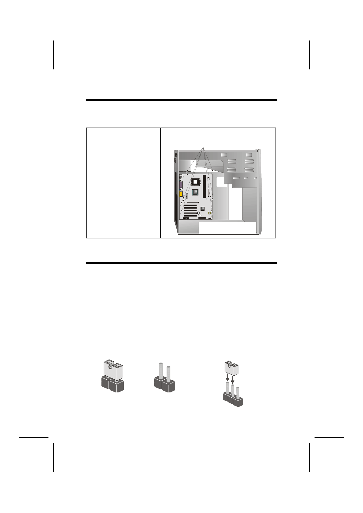
IInnssttaalllliinngg tthhee MMaaiinnbbooaarrdd iinn aa CCaassee
Refer to the following illustration and instructions for installing the mainboard
in a case:
This illustration shows an example of a mainboard being
installed in a tower-type case:
Note: Do not overtighten
the screws as this
can stress the mainboard.
Most system cases have
mounting brackets i nstalled in
the case, which correspond to
the holes in the mainboard.
Place the mainboard over the
mounting brackets and secure
the mainboard onto the mount ing brackets with screws.
2. Secure the mainboard with
screws where approp ria t e .
1. Place the mainboard
over the mounting brackets.
Ensure that your case has an I/O template that supports the I/O ports and
expansion slots on your mainboard.
CChheecckkiinngg JJuummppeerr SSeettttiinnggss
This section explains how to set jumpers for correct configuration of the mainboard.
Setting Jumpers
Use the mainboard jumpers to set system configuration options. Jumpers with
more than one pin are numbered. When setting the jumpers, ensure that the
jumper caps are placed on the correct pins.
The illustrations below show a 2-pin jumper.
When the jumper cap is placed on both pins,
the jumper is SHORT. If you remove the
jumper cap, or place the jumper cap on just
one pin, the jumper is OPE N.
Short Open
This illustration shows a 3-pin
jumper. Pins 1 and 2 are SHORT.
1
2
3
8
Page 13
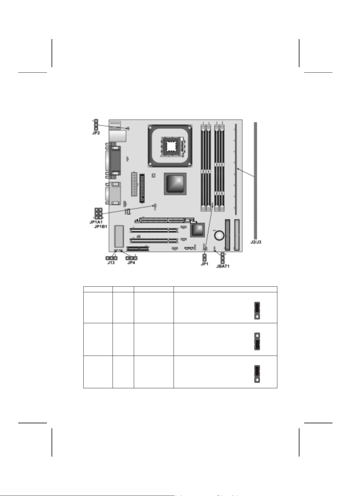
Checking Jumper Settings
The following illustration shows the location of the mainboard jumpers. Pin 1 is
labeled.
Jumper Settings
Jumper Type Description Setting (default)
JBAT1 3-pin Clear CMOS 1-2: Normal
2-3: Clear
JP1A1 3-pin CPU Clock 100M: Short Pins 1-2
133M: Short Pins 1-2
JP1B1 3-pin CPU Clock 100M: Short Pins 2-3
133M: Short Pins 1-2
9
JBAT1
1
JP1A1
1
JP1B1
1
Page 14
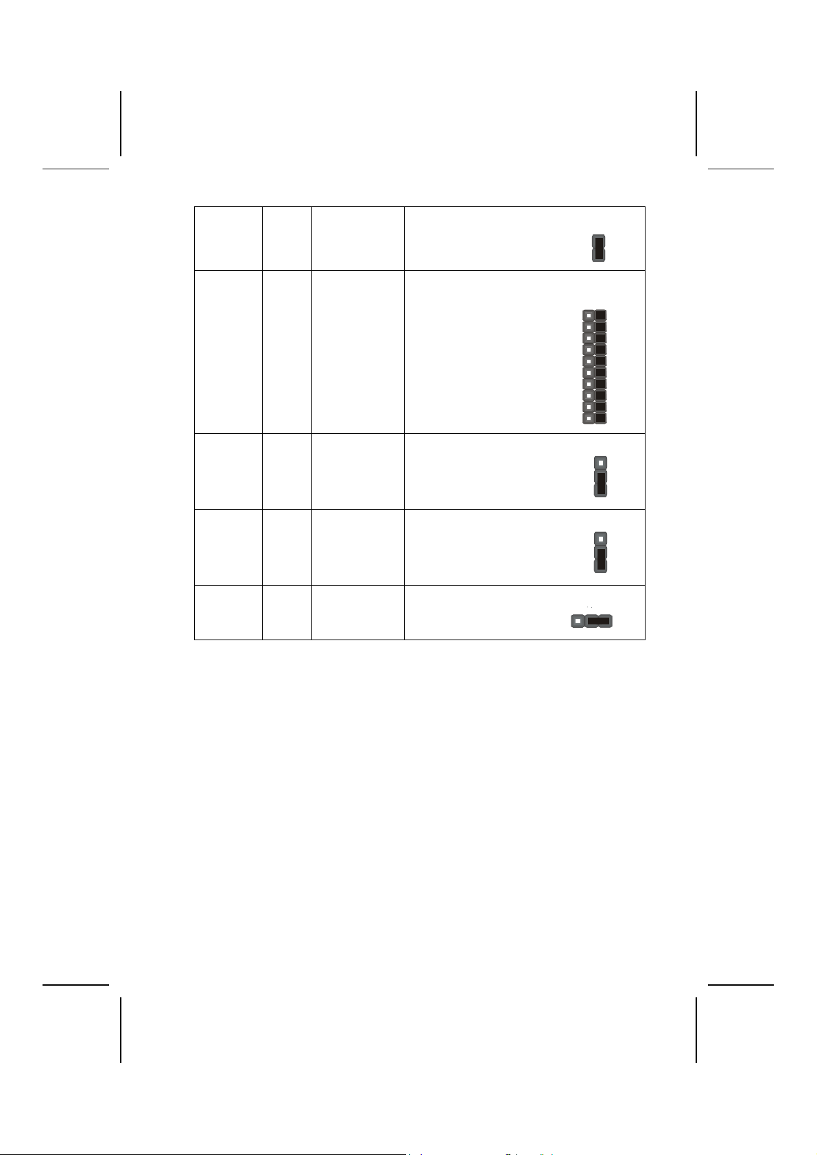
JP1 2-pin DRAM Voltage
J2A/B/C/D
J3A/B/C/D
JP2 3-pin Keyboard
J13 3-pin Flash ROM
JP4 3-pin Flash ROM
20-pin DDR/SDR
(VCC)
DRAM Type
Selector
Power On
Voltage (VCC)
Size
2.5V (DDR): Open Pins 1-2
3V (SDR): Short Pins 1-2
DDR1, DDR2:
Short all J2A/B/ C/D and
J3A/B/C/D pins
DIMM1, DIMM2:
Open all J2A/B/C/D and
J3A/B/C/D pins
5V: Short Pins 1-2
5VSB: Short Pins 2-3
5V: Short Pins 1-2
3V: Short Pins 2-3
2M: Short Pins 1-2
4M: Short Pins 2-3
JP1
J2A/B/C/D
J3A/B/C/D
JP2
1
J13
1
JP4
1
JBAT1
This jumper is to clear the contents of CMOS memory. You may need to clear
the CMOS memory if the settings in the Setup Utility are incorrect that prevents your mainboard from operating. To clear the CMOS memory, disconnect
all the power cables from the mainboard and then move the jumper cap into
the CLEAR setting for a few seconds. This jumper enables you to reset BIOS.
JP1A1/ JP1B1
This jumper enables you to select the CPU frequency. Both jumpers should
be set concurrently.
JP1: DRAM Voltage (VCC)
This jumper enables to select voltage of DRAM.
J2A/B/C/D, J3A/B/C/D: DDR/SDR DRAM Type Selector
This jumper enables to select the type of DDR or SDR DRAM.
10
Page 15

JP2: Keyboard Power On
This jumper enables any keyboard activity to power up a system previously in
a standby or sleep state.
J13: Flash ROM Voltage (VCC)
This jumper enables to select voltage of flash ROM.
JP4: Flash ROM Size
This jumper enables to select size of flash ROM.
CCoonnnneeccttiinngg CCaassee CCoommppoonneennttss
After you have installed the mainboard into a case, you can begin connecting
the mainboard components. Refer to the following:
1. Connect the case
power supply
connector to CN5.
2. Connect the CPU
cooling fan cable to
CPU_FAN.
3. Connect the case
cooling fan connector
to SYSTEM_FAN.
4. Connect the case
speaker cable to
SPEAKER1.
5. Connect the case
switches and indicator
to PANEL1/
PANEL2.
CN5: ATX 20-pin Power Connector
Pin Signal Name Pin Signal Name
1 +3.3V 11 +3.3V
2 +3.3V 12 -12V
3 Ground 13 Ground
4 +5V 14 PS ON#
5 Ground 15 Ground
6 +5V 16 Ground
7 Ground 17 Ground
8 PWRGD 18 +5V
9 +5VSB 19 +5V
10 +12V 20 +5V
11
Page 16

CPU_FAN1/SYSTEM_FAN: FAN Power Connectors
Pin Signal Name Function
1 GND System Ground
2 +12V Power +12V
3 Sense Sensor
SPEAKER1: Internal speaker
Pin Signal Name
1 SPKR
2 NC
3 GND
4 +5V
J12: Sleep Switch
This header is connected to the sleep button for suspending the computer’s
activity if pushing the button. Or, the computer is automatically suspended
after passing a period of time.
Pin Signal Name
1 -EXTSMI
2 GND
The Panel Connectors
PANEL1
If there is a headphone jack or a microphone jack on the front panel, connect
the cables to the PANEL1 on the mainboard.
10 9
Pin Signal Name Pin Signal Name
1 MIC IN 2 GND
3 VCCMIC 4 +5V AUDIO
5 LINE OUT (R) 6 LI NE OUT (R)
7 NC 8 EMPTY
9 LINE OUT (L) 10 LINE OUT (L)
12
2 1
Page 17

h
PANEL2
This panel connector provides a set of switch and LED connectors found on
ATX case. Refer to the table below for information.
Empty
(Pin 10)
10 9
N/C
(Pin 9)
Reset Switc
(Pins 5, 7)
HDD LED
(Pins 1, 3)
Pin Signal Name Pin Signal Name
+1 HDD LED +2 SPD-LED Indicator
-3 HDD LED 4 SPD-LED Indicator
5 Reset Switch 6 POWER ON/OFF
7 Reset Switch 8 POWER ON/OFF
9 NC 10 EMPTY
Power Switch
(Pins 6, 8)
SPD- LED
(Pins 2, 4)
2 1
J16: LAN LED Indicator
This connector is attached to LAN device that needs a LED indicator.
Device Pins
Link LED 1, +2
ACT LED +3, 4
1
+
+
4
LINK LED
ACT LED
Note: The plus sign (+) indicates a pin which must be connected to a positive
voltage.
13
Page 18

IInnssttaalllliinngg HHaarrddwwaarree
Installing the Processor
Caution: When install i ng a CP U heatsink and cooling fan make sure that
you DO NOT scratch the mainboard or any of the surface-mount resistors
with the clip of the cooling fan. If the clip of the cooling fan scrapes
across the mainboard, you may cause serious damage to the mainboard
or its components.
On most mainboards, there are small surface-mount resi stors near the
processor socket, which may be damaged if the cooling fan is carelessly
installed.
Avoid using cooling fans with sharp edges on the fan casing and the
clips. Also, install the cooling fan in a well-l i t work area so that you can
clearly see the mainboard and processor socket.
Before installing the Processor
This mainboard automatically determines the CPU clock frequency and system bus frequency for the processor. You may be able to change these
settings by making changes to jumpers on the mainboard, or changing the
settings in the system Setup Utility. We strongly recommend that you do not
overclock processors or other components to run faster than their rated speed.
Warning: Overclocking components can adversely affect the reliability of
the system and introduce errors into your system. Overclocking can permanently damage the mainboard by generating excess heat in
components that are run beyond the rated limits.
This mainboard has a mPGA478 socket. When choosing a processor, consider the performance requirements of the system. Performance is based on
the processor design, the clock speed and system bus frequency of the processor, and the quantity of internal cache memory and external cache memory.
14
Page 19

CPU Installation Procedure
The following illustration shows CPU installation components:
Note: The pin-1 corner is marked with an arrow
Follow these instructions to install the Retention Module and CPU:
1. Remove the existing retention module (if applicable).
2. Position the backplate
against the underside of
the mainboard, secure
the 4 screws firmly on
the retention module.
Note: Do not over tighten
the screws.
3. Install your CPU. Pull up
the lever away from the
socket and lift up to 90degree angle.
15
Page 20

4. Locate the CPU cut
edge (the corner with the
pinhole noticeably missing). Align and insert the
CPU correctly.
5. Press the lever down.
6. Apply thermal grease on top of the CPU.
7. Put the CPU Fan down
on the retention module
and snap the four retention legs of the cooling
fan into place.
8. Flip the levers over to lock the heat sink in place.
9. Connect the CPU Cooling Fan power cable to
the CPUFAN1 connector. This completes the
installation.
To achieve better airflow rates and heat dissipation, we suggest that
Notes:
•
you use a high quality fan with 4800 rpm at l east.
• CPU fan and heatsink installation procedures may vary with the type of
CPU fan/heatsink suppl i ed. The form and size of fan/heatsink may also
vary.
16
Page 21

Installing Memory Modules
This mainboard accommodates 168-pin 3.3V/184-pin 2.5V unbuffered
SDRAM memory modules. The memory chips must be standard or registered
SDRAM (Synchronous Dynamic Random Access Memory).
The CPU supports 100MHz system bus. The SDRAM DIMMs and DDRs can
synchronously work with 100 MHz or operates over a 266 MHz system bus.
DDR SDRAM provides 800 MBps or 1 GBps data transfer depending on
whether the bus is 100 MHz or 266 MHz. It doubles the rate to 1.0 GBps and
2.1 GBps by transferring data on both the rising and falling edges of the clock.
DDR SDRAM uses additional power and ground lines and requires 184-pin
2.5V unbuffered DIMM module rather than the 168-pin 3.3V unbuffered
DIMMs used by SDRAM.
Do not remove any memory module from its ant i static packaging until
you are ready to install it on the mainboard. Handle the modules only by
their edges. Do not touch the components or metal parts. Always wear
a grounding strap when you handle the modules.
Note: You must install at least one memory module in order to work out this
mainboard, either SDRAM or DDR SDRAM, but you can’t use them
simultaneously.
Refer to the following to install the memory modules.
1. Push the latches on each side of the DIMM slot down.
2. Align the memory module with the slot. The DIMM slots are keyed with
notches and the DIMMs are keyed with cutouts so that they can only be
installed correctly.
3. Check that the cutouts on the DIMM module edge connector match the
notches in the DIMM slot:
17
Page 22

Latch
Cutout
Notch
Latch
DDR SDRAM Module SDRAM Module
Latch
Notches
Cutouts
Latch
4. Install the DIMM module into the slot and press it firmly down until it
seats correctly. The slot latches are levered upwards and latch on to the
edges of the DIMM.
5. Install any remaining DIMM modules.
Installing a Hard Disk Drive/CD-ROM
This section describes how to install IDE devices such as a hard disk drive
and a CD-ROM drive.
About IDE Devices
Your mainboard has a primary and secondary IDE channel interface (IDE1 and
IDE2). An IDE ribbon cable supporting two IDE devices is bundled with the mainboard.
If you want to install more than two IDE devices, get a second IDE cable and
you can add two more devices to the secondary IDE channel.
IDE devices have jumpers or switches that are used to set t he IDE device as
MASTER or SLAVE. Refer to the IDE device user’s manual. When installing two
IDE devices on one cable, ensure that one device is set to MASTER and the
other device is set to SLAVE. The documentation of your IDE device explains
how to do this.
About UltraDMA
This mainboard supports UltraDMA 66/100/133. UDMA is a technology that
accelerates the performance of devices in the IDE channel. To maximize performance, install IDE devices that support UDMA and use 80-pin IDE cables
that support UDMA 66/100133.
18
Page 23

Installing a Hard Disk Drive
1. Install the hard disk dri ve i nto the drive cage in your system case.
2. Plug the IDE cable into IDE 1
(A):
Note: Ribbon cable connectors
are usually keyed so that they c an
only be installed correct l y on the
device connector. If the connector
is not keyed, mak e sure that you
match the pin-1 side of t he cable
connector with the pin-1 side of the
device connector. Each connector
has the pin-1 side clearly m arked.
The pin-1 side of each ribbon cable is always marked with a
colored stripe on the cable.
3. Plug an IDE cable connector i nto the hard disk drive IDE connector (B). It
doesn't matter which connector on the cable you use.
4. Plug a power cable from the case power supply i nto the power connector on
the hard disk drive (C).
When you first start up your system, the BIOS should automatically detect
your hard disk drive. If it doesn’t, enter the Setup Utility and use the IDE Hard
Disk Auto Detect feature to configure the hard disk drive that you have installed.
Installing a CD-ROM/DVD Drive
1. Install the CD-ROM/DVD drive into t he dri ve cage in your system case.
2. Plug the IDE cable into IDE 1
(A). If you have already installed
an HDD, use the other connector on the IDE cable.
Note: Ribbon cable connectors are
usually keyed so that they can only
be installed correctly on the device
connector. If the c onnector is not
keyed, make sure that you match the
pin-1 side of the cable connector with
the pin-1 side of the device connector. Each connector has the pin-1
side clearly marked. The pin-1 side of
each ribbon cable is always marked
with a colored stripe on the cable.
3. Plug an IDE cable connector i nto the CD-ROM/DVD drive IDE connector (B). It
doesn't matter which connector on the cable you use.
4. Plug a power cable from the case power supply i nto the power connector on
the CD-ROM/DVD drive (C).
5. Use the audio cable provided with the CD-ROM/DVD drive to connect to the
mainboard CD-in connector CDIN1 or CDIN2 (D).
When you first start up your system, the BIOS should automatically detect
your CD-ROM/DVD drive. If it doesn’t, enter the Setup Utility and configure
the CD-ROM/DVD drive that you have installed.
19
Page 24

Installing a Floppy Diskette Drive
The mainboard has a floppy diskette drive (FDD) interface and ships with a
diskette drive ribbon cable that supports one or two floppy diskette drives. You
can install a 5.25-inch drive and a 3.5-inch drive with various capacities. The
floppy diskette drive cable has one type of connector for a 5.25-inch drive and
another type of connector for a 3.5-inch drive.
1. Install the FDD into the dri ve c age i n your system case.
2. Plug the FDD cable into
FLOPPY1 (A):
Note: Ribbon cable connectors are
usually keyed so that they can only
be installed correctly on the device
connector. If the c onnector is not
keyed, make sure that you match the
pin-1 side of the cable connector with
the pin-1 side of the device connector. Each connector has the pin-1
side clearly marked. The pin-1 side of
each ribbon cable is always marked
with a colored stripe on the cable.
3. Plug the correct connector on the FDD cable for the 5.25-inch or 3. 5-i nch drive
into the FDD connector (B).
4. Plug a power cable from the case power supply i nto the power connector on
the FDD (C).
When you first start up your system, go immediately to the Setup Utility to
configure the floppy diskette drives that you have installed.
20
Page 25

Installing Add-on Cards
The slots in this mainboard are designed to hold expansion cards and connect
them to the system bus. Expansion slots are a means of adding or enhancing
the mainboard’s features and capabilities. With these efficient facilities, you
can increase the mainboard’s capabilities by adding hardware which performs
tasks that are not part of the basic system.
PCI Slots
4xAGP Slot
CNR Slot
Note: Before installing an add-on card, check the documentation for the card
carefully. If the card is not Plug and Play, you may have to manually configure the card before installation.
PCI slots are used to i nstall expansion cards that have the 32-bit
PCI interface.
The AGP slot is used t o install a graphics adapter that supports the
4xAGP specification and has a 4xAGP edge connector.
Note: The above layout is for reference only. The AGP slot
may be different from your mainboard. Please refer to
actual shipment.
This slot is used to i nsert CNR cards with Modem and Audio func tionality.
21
Page 26

Follow these instructions to install an add-on card:
1. Remove a blanking plate from the system cas e corresponding to the slot you
are going to use.
2. Install the edge connect or of the
add-on card into the expansion
slot. Ensure that t he edge connector is correctly seated in the
slot.
3. Secure the metal bracket of the card to the system case with a screw.
Note: For some add-on cards, for example graphics adapters and network adapters,
you have to insta ll drive rs a nd sof tw are bef ore y ou can be gin us ing the add-on
card.
22
Page 27

Connecting Optional Devices
Refer to the following for information on connecting the mainboard’s optional
devices:
USB1/USB2: Front panel USB ports
The mainboard has two USB ports installed on the rear edge I/O port array.
Additionally, some computer cases have USB ports at the front of the case. If
you have this kind of case, use auxiliary USB connectors USB1 and USB2 to
connect the front-mounted ports to the mainboard.
Pin Signal Name Function
1 VREG_FP_USBPWR0 Front Panel USB Power
2 VREG_FP_USBPWR0 Front Panel USB Power
3 USB_FP_P0- USB P ort 0 Negative Signal
4 USB_FP_P1- USB P ort 1 Negative Signal
5 USB_FP_P0+ USB Port 0 Positive Signal
6 USB_FP_P1+ USB Port 1 Positive Signal
7 GND Ground
8 GND Ground
9 KEY No pin
10 USB_FP_OC0 Overcurrent signal
23
Page 28

Note: Please make sure th at the USB cable has the same pin assignment as indi-
cated above. A different pin assignment may cause damage or system
hang-up.
WOL1: Wake On LAN
If you have installed a LAN card, use the cable provided with the card to plug
into the mainboard WOL1 connector. This enables the Wake On LAN (W OL)
feature. When your system is in a power-saving mode, any LAN signal automatically resumes the system. You must enable this item using the Power
Management page of the Setup Utility.
Pin Signal Name Function
1 5VSB +5V stand by power
2 GND Ground
3 Ring# Wake up signal (high active)
WOM1: Wake On Modem
If you have installed a modem, use the cable provided with the modem to plug
into the mainboard WOM1 connector. This enables the Wake On Modem
(WOM1 feature. When your system is in a power-saving mode, any modem
signal automatically resumes the system. You must enable this item using the
Power Management page of the Setup Utility. See Chapter 3 for more information.
Pin Signal Name Function
1 5VSB +5V stand by power
2 GND Ground
3 Ring# Wake up signal (low active)
SIR1: Serial infrared port
The mainboard supports a Infrared (IR1) data port. Infrared ports allow the
wireless exchange of information between your computer and similarly
equipped devices such as printers, laptops, Personal Digital Assistants
(PDAs), and other computers.
Pin Signal Name Function
1 Not assigned Not as signed
2 KEY No pin
3 +5V IR Power
4 GND Ground
5 IRTX IrDA serial output
6 IRRX IrDA serial input
24
Page 29

CCoonnnneeccttiinngg II//OO DDeevviicceess
The backplane of the mainboard has the following I/O ports:
PS/2
mouse
PS/2
keyboard
PS/2 Mouse
PS/2 Keyboard
USB Ports
LAN Port
LAN
port
USB
ports
Parallel port (LPT1)
Serial port
COM 1
Use the upper PS/2 port to connect a PS/2 pointing device.
Use the lower PS/2 port to connec t a PS/2 keyboard.
Use the USB ports to connect USB devices.
Use the LAN port to connect t o t he network.
VGA
Game port
(optional)
LPT1
COM1
Game Port
Audio Ports
VGA Port
Use LPT1 to connect printers or other parallel communic ations devices.
Use the COM ports to connect serial devi ces such as mice
or fax/modems. COM1 is identified by the system as
COM1/3.
Use the game port to connect a joystick or a MIDI devi ce.
Use the three audio ports to connect audi o devi ces. The left
side jack is for a stereo line-out signal. The middle jack is for
a stereo line-in signal. The right si de j ack is for a microphone.
Use the VGA port to connect graphic display devi ces.
Microphone
Line-in
Line-out
PS/2 Mouse
Use the upper PS/2 port to connect a PS/2 pointing device.
25
Page 30

External Connector Color Coding
Many connectors now use standard colors as shown in the table below.
Connector
Audio line-in Light blue
Audio line-out Lime
Digital monitor/f l at panel White
IEEE 1394 Grey
Microphone Pink
MIDI/game Gold
Parallel Burgundy
PS/2-compatibl e keyboard Purple
PS/2-compatible mouse Green
Serial Teal or Turquoise
Speaker out/subwoofer Orange
Right-to-left speaker Brown
USB Black
SCSI, network, telephone, modem None
This concludes Chapter 2. The next chapter covers the BIOS.
Color
26
Page 31

CChhaapptteerr 33
Using BIOS
AAbboouutt tthhee SSeettuupp UUttiilliittyy
The computer uses the latest AMI BIOS with support for Windows Plug and
Play. The CMOS chip on the mainboard contains the ROM setup instructions
for configuring the mainboard BIOS.
The BIOS (Basic Input and Output System) Setup Utility displays the system's
configuration status and provides you with options to set system parameters.
The parameters are stored in battery-backed-up CMOS RAM that saves this
information when the power is turned off. When the system is turned back on,
the system is configured with the values you stored in CMOS.
The BIOS Setup Utility enables you to configure:
• Hard drives, diskette drives, and peripherals
• Video display type and display options
• Password protection from unauthorized use
• Power management features
The settings made in the Setup Utility affect how the computer performs. Before using the Setup Utility, ensure that you understand the Setup Utility
options.
This chapter provides explanations for Setup Utility options.
The Standard Configuration
A standard configuration has already been set in the Setup Utility. However,
we recommend that you read this chapter in case you need to make any
changes in the future.
This Setup Utility should be used:
• when changing the system configuration
• when a configuration error is detected and you are prompted to
make changes to the Setup Utility
• when trying to resolve IRQ conflicts
• when making changes to the Power Management configuration
• when changing the password or making other changes to the Secu-
rity Setup
27
Page 32

Entering the Setup Utility
When you powe r on the system , BIOS e nters t he Powe r-On Se lf Test (POST)
routines. POST is a series of built-in diagnostics performed by the BIOS. After
the POST routines are completed, the following message appears:
Press DEL to enter SETUP
Pressing the delete key
AMIBIOS SIMPLE SETUP UTILITY – VERSION 1.21.06
©2000 American Megatrends, Inc. All Rights Reserved
Standard CMOS Setup
Advanced Setup
Power Management Setup
PCI / Plug and Play Setup
Load Optimal Settings
Load Best Performance Settings
Esc : Quit ↑ ↓ ← →: Select Item (Shift)F2 : Change Color F5 : Old Values
F6 : Optimal values F7 : Best performance values F10 : Save&Exit
Standards COMOS setup for changing ti me, date, hard disk type, etc.
BIOS Navigation Keys
accesses the BIOS Setup Utility:
Features Setup
CPU PnP Setup
Hardware Monitor
Change Password
Exit
The BIOS navigation keys are listed below:
Key Function
Esc Exits the current menu
←↑↓→
+/–/PU/PD Modifi es the selected field's values
F10 Saves the current configuration and exits setup
F1 Displays a screen that describes al l key functions
F5 Loads previous l y saved values to CMOS
F6 Loads a minimum configuration for troubleshooting.
F7 Loads an opti mum set of values for peak performance
UUssiinngg BBIIOOSS
Scrolls through the items on a menu
When you start the Setup Utility, the main menu appears. The main menu of
the Setup Utility displays a list of the options that are available. A highlight
indicates which option is currently selected. Use the cursor arrow keys to
move the highlight to other options. When an option is highlighted, execute
the option by pressing <Enter>.
Some options lead to pop-up dialog boxes that prompt you to verify that you
wish to execute that option. Other options lead to dialog boxes that prompt
you for information.
28
Page 33

Some options (marked with a triangle ) lead to submenus that enable you
to change the values for the option. Use the cursor arrow keys to scroll
through the items in the submenu.
In this manual, default values are enclosed in parenthesis. Submenu items
are denoted by a triangle .
Standard CMOS Features
This option displays basic information about your system.
AMIBIOS SETUP – STANDARD CMOS SETUP
©2000 American Megatrends, Inc. All Rights Reserved
Date (mm/dd/yy) : Mon Nov 04, 2002
Time (hh/mm/ss) : 15:28:50
LBA Blk PIO 32Bit
Type Size Cyln Head WPcom Sec Mode Mode Mode Mode
Pri Master : Auto On
Pri Slave : Auto On
Sec Master : Auto On
Sec Slave : Auto On
Floppy Drive A : 1.44 MB 31/2
Floppy Drive B : Not Instal led
Month : Jan – Dec ESC : Exit
Day : 01 – 31 ↑↓ : Select Item
Year : 1901 – 2099 PU/PD/+/- : Modify
(Shift)F2 : Color
F3 : Detect All HDD
Date and Time
The Date and Time items show the current date and time on the computer. If
you are running a Windows OS, these items are automatically updated whenever you make changes to the Windows Date and Time Properties utility.
IDE Pri Master/Pri Slave/Sec Master/Sec Slave
Use these items to configure devices connected to the Primary and Secondary IDE channels. To configure an IDE hard disk drive, choose Auto. If the
Auto setting fails to find a hard disk drive, set it to User, and then fill in the
hard disk characteristics (Size, Cyls, etc.) manually. If you have a CD-ROM
drive, select the setting CDROM. If you have an ATAPI device with removable
media (e.g. a ZIP drive or an LS-120), select Floptical.
Floppy Drive A/Floppy Drive B
Use these items to set up size and capacity of the floppy diskette drive(s) installed in the system.
29
Page 34

Advanced Setup Page
This option defines advanced information about your system.
AMIBIOS SETUP – ADVANCED SETUP
©2000 American Megatrends, Inc. All Rights Reserved
Quick Boot Enabled
st
1
Boot Device IDE-0
nd
2
Boot Device Floppy
rd
Boot Device CDROM
3
Try Other Boot Devices Yes
S.M.A.R.T. for Hard Disks Disabl ed
BootUp Num-Lock On
Floppy Drive Swap Disabled
Floppy Drive Seek Disabled
Password Check Setup
Boot To OS/2 No
L2 Cache Enabled
System BIOS Cacheable Enabled
SDRAM Timing by SPD Disables
SDRAM Frequency 100MHz
SDRAM CAS# Latency 2.5
SDRAM Bank Interleave Disabled
AGP Mode 4X
AGP Comp. Driving Auto
AGP Comp. Driving CB
Manual
Quick Boot
If you enable this item, the system starts up more quickly be elimination some
of the power on test routines.
AGP Aperture Size 64MB
Auto detect DIMM/PCI Clk Enabled
CLK Gen Spread Spectrum Disabled
Hyper Threading Function Disabled
ESC : Quit ↑↓←→ : Select Item
F1 : Help PU/PD/+/- : Modify
F5 : Old Values (Shift)F2 : Color
F6 : Load BIOS Defaults
F7 : Load Setup Defaults
1st Boot Device/2nd Boot Device/3rd Boot Device
Use these items to determine the device order the computer uses to look for
an operating system to load at start-up time.
Try Other Boot Device
If you enable this item, the system will also search for other boot devices if it
fails to find an operating system from the first two locations.
S.M.A.R.T. for Hard Disks
Enable this item if any IDE hard disks support the S.M.A.R.T. (Self-Monitoring,
Analysis and Reporting Technology) feature.
BootUp Num-Lock
This item determines if the Num Lock key is active or inactive at system startup time.
Floppy Drive Swap
If you have two diskette drives installed and you enable this item, drive A becomes drive B and drive B becomes drive A.
Floppy Drive Seek
If you enable this item, your system will check all floppy disk drives at start up.
Disable this item unless you are using an old 360KB drive.
30
Page 35

Password Check
If you have entered a password for the system, use this item to determine, if
the password is required to enter the Setup Utility (Setup) or required both at
start-up and to enter the Setup Utility (Always).
Boot to OS/2 > 64MB
Enable this item if you are booting the OS/2 operating system and you have
more than 64MB of system memory installed.
L2 Cache
Leave these items enabled since all the processors that can be installed on
this board have internal L2 cache memory.
System BIOS Cacheable
If you enable this item, a segment of the system BIOS will be copied to main
memory for faster execution.
DOS Flat Mode
This item enables BIOS to enter the DOS protected mode without other software supporting under the DOS operating system. W e recommend you leave
this item at the default value.
SDRAM Timing By SPD
This item allows you to enable or disable the SDRAM timing defined by the
Serial Presence Detect electrical.
SDRAM Frequency
This item determines frequency of SDRAM memory.
SDRAM CAS# Latency
This item determines the operation of SDRAM memory CAS (column address
strobe). It is recommended that you leave this item at the default value. The
2T setting requires faster memory that specifically supports this mode.
SDRAM Bank Interleave
Enable this item to increase SDRAM memory speed. When enabled, separate
memory banks are set for odd and even addresses and the next byte of
memory can be accessed while the current byte is being refreshed.
AGP Comp. Driving
Use this item to signal driving current on AGP cards to auto or manual. Some
AGP cards need stronger than normal driving current in order to operate. We
recommend that you set this item to the default.
Manual AGP Comp. Driving
When AGP Driving is set to Manual, use this item to set the AGP current driving value.
AGP Mode
This item provides the OnBoard VGA mode with three options of 1,2, 4 multiplied frequency.
31
Page 36

AGP Aperture Size
This item defines an AGP for the graphics. Leave this item at the default value
64MB.
Auto detect DIMM/PCI Clock
When this item is enabled, BIOS will disable the clock signal of free DIMM/PCI
slots.
CLK GEN Spread Spectrum
Use this item to set the system bus spread spectrum for the installed processor.
Hyper Threading Function
This item is dependent when your system supports the Hyper-Threading
technology. If your system does not have the Hyper-Threading technology
installed, this item is hidden.
Power Management Setup Page
This page sets up some parameters of system power management operation.
AMIBIOS SETUP – POWER MANAGEMENT SETUP
©2000 American Megatrends, Inc. All Rights Reserved
ACPI Aware O/S Yes
Power Management Enabled
Suspend Time Out Disabled
Hard Disk Time Out Standby
Resume On RTC Alarm Disabled
RTC Alarm Date 15
RTC Alarm Hour 12
RTC Alarm Minute 30
RTC Alarm Second 30
LAN/Ring Power On Disabled
Keyboard Power On Disabled
Wake-Up Key Any key
Wake-Up Password N/A
ESC : Quit ↑↓←→ : Select Item
F1 : Help PU/PD/+/- : Modify
F5 : Old Values (Shift)F2 : Color
F6 : Load BIOS Defaults
F7 : Load Setup Defaults
ACPI Aware O/S
This item supports ACPI (Advanced Configuration and Power management
Interface). Use this item to enable or disable the ACPI feature.
Power Management
Use this item to enable or disable a power management scheme. If you enable power management, you can use the items below to set the power
management operation. Both APM and ACPI are supported.
Suspend Time Out
This sets the timeout for Suspend mode in minutes. If the time selected
passes without any system activity, the computer will enter power-saving Suspend mode.
32
Page 37

Hard Disk Time Out
This item sets up the timeout to power down the hard disk drive, if there is no
hard disk activity after passing the preset period of time.
Resume On RTC Alarm / Date / Hour / Minute / Second
The system can be turned off with a software command. If you enable this
item, the system can automatically resume at a fixed time based on the system’s RTC (realtime clock). Use the items below this one to set the date and
time of the wake-up alarm. You must use an ATX power supply in order to use
this feature.
LAN/Ring Power On
The system can be turned off with a software command. If you enable this
item, the system can automatically resume if there is an incoming call on the
Modem. You must use an ATX power supply in order to use this feature.
Keyboard Power On /Wake-Up Key/Wake-Up/ Password
If you enable this item, system can automatically resume by pressing hot
keys on the keyboard or typing in the password. You must enable the Keyboard Power On jumper and use an ATX power supply in order to use this
feature.
PCI / Plug and Play Setup Page
This page s ets up some pa rameters for devic es install ed on the P CI bus and
those utilizing the system plug and play capability.
AMIBIOS SETUP – PCI / PLUG AND PLAY SETUP
©2000 American Megatrends, Inc. All Rights Reserved
Plug and Play Aware O/S Yes
Share Memory Size 32MB
Primary Graphics Adapter PCI
Allocate IRQ for PCI VGA Yes
PCI IDE BusMaster Disabled
ESC : Quit ↑↓←→ : Select Item
F1 : Help PU/PD/+/- : Modify
F5 : Old Values (Shift)F2 : Color
F6 : Load BIOS Defaults
F7 : Load Setup Defaults
Plug and Play Aware O/S
Enable this item if you are using an O/S that supports Plug and Play such as
Windows 95 or 98.
Share Memory Size
This item lets you allocate a portion of the main memory for the onboard VGA
display application with three options of 8/16/32MB.
Primary Graphics Adapter
This item indicates if the primary graphics adapter uses the PCI or the AGP
bus. The default AGP setting still lets the onboard display work and allows the
33
Page 38

use of a second display card installed in an AGP slot.
Allocate IRQ for PCI VGA
If this item is enabled, an IRQ will be assigned to the PCI VGA graphics system. You set this value to No to free up an IRQ.
PCI IDE BusMaste r
This item enables or disables the DMA under DOS mode. We recommend you
to leave this item at the default value.
Load Optimal Settings
If you select this item and press Enter a dialog box appears. If you press Y,
and then Enter, the Setup Utility loads a set of fail-safe default values. These
default values are not very demanding and they should allow your system to
function with most kinds of hardware and memory chips.
Note: It is highly recommended that users enter this option to load optimal
values for accessing the best performance.
Load Best Performance Settings
If you select this item and press Enter a dialog box appears. If you press Y,
and then Enter, the Setup Utility loads a set of best-performance default values. These default values are quite demanding and your system might not
function properly if you are using slower memory chips or other lowperformance components.
Features Setup Page
This page s ets up so m e par am e t e rs fo r th os e p eri p he r al devi c e s c onn e c te d to
the system.
AMIBIOS SETUP – FEATURES SETUP
©2000 American Megatrends, Inc. All Rights Reserved
OnBoard FDC Enabled
OnBoard Serial PortA 3F8h/COM1
OnBoard IR Port Disabled
OnBoard Parallel Port 378h
Parallel Port Mode SPP
Parallel Port IRQ 7
Parallel Port DMA N/A
OnBoard Game Port 201h
OnBoard MIDI Port 300h
MIDI Port IRQ 10
OnBoard IDE Both
Audio Device Enabled
Modem Device Auto
Ethernet Device Enabled
USB Controller Enabled
USB Device Legacy Support Disabled
ThumbDrive Support for DOS Disabled
ESC : Quit ↑↓←→ : Select Item
F1 : Help PU/PD/+/- : Modify
F5 : Old Values (Shift)F2 : Color
F6 : Load BIOS Defaults
F7 : Load Setup Defaults
34
Page 39

OnBoard FDC
Use this item to enable or disable the onboard floppy disk drive interface.
OnBoard Serial PortA
Use this item to enable or disable the onboard COM1 serial port, and to assign a port address.
OnBoard IR Port
Use this item to enable or disable the onboard infrared port, and to assign a
port address.
Parallel Port Mode
Use this item to set the parallel port mode. You can select SPP (Standard
Parallel Port), ECP (Extended Capabilities Port), EPP (Enhanced Parallel
Port), or ECP + EPP.
Parallel Port IRQ
Use this item to assign IRQ to the parallel port.
Parallel Port DMA
Use this item to assign a DMA channel to the parallel port.
OnBoard Game Port
This item enables or disables the I/O address for the game port.
OnBoard MIDI Port
Use this item to enable or disable the onboard MIDI port, and to assign a port
address.
MIDI Port IRQ
Use this item to assign IRQ 7 to the parallel port.
OnBoard IDE
Use this item to enable or disable the onboard IDE channel.
Audio Device
This item enables or disables the AC’97 audio chip.
Modem Device
This item enables or disables the MC’97 modem chip.
Ethernet Device
This item enables or disables the onboard Ethernet LAN.
USB Controller
Use this item to select the USB ports or disabled.
USB Device Legacy Support
This item allows you to enable the USB device, if you have installed a USB
device on the system board.
35
Page 40

ThumbDrive Support For DOS
Enable this item to make a small portion of memory storage device for the
USB ports.
CPU PnP Setup Page
This page helps you manually configure the mainboard for the CPU. The system will automatically detect the type of installed CPU and make the
appropriate adjustments to the items on this page.
AMIBIOS SETUP – CPU PnP SETUP
©2000 American Megatrends, Inc. All Rights Reserved
CPU BRAND INTEL
CPU Type Pentium 4
CPU Ratio 8.0x
CPU Frequency 100 MHz
ESC : Quit ↑↓←→ : Select Item
F1 : Help PU/PD/+/- : Modify
F5 : Old Values (Shift)F2 : Color
F6 : Load BIOS Defaults
F7 : Load Setup Defaults
CPU BRAND/Type/ Core Voltage/Ratio /Frequency
These items show the type, core voltage, ratio and frequency of CPU installed
in your system.
Hardware Monitor Page
On mainboards that support hardware monitoring, this item lets you monitor
the parameters for critical voltages, critical temperatures, and fan speeds:
AMIBIOS SETUP – HARDWARE MONITOR
©2000 American Megatrends, Inc. All Rights Reserved
*** System Hardware ***
Vcore 1.632V
Vcc 2.5V 2.496V
Vcc 3.3V 3.392V
Vcc 5V 4.945V
+12V 11.968V
-12V 11.968V
SB5V 5.026V
VBAT 3.488V
SYSTEM Fan Speed 0 RPM
CPU Fan Speed 1298 RPM
Power Temperature 33°C/91°F
SYSTEM Temperature 39°C/102°F
CPU Temperature 55°C/131°F
ESC : Quit ↑↓←→ : Select Item
F1 : Help PU/PD/+/- : Modify
F5 : Old Values (Shift)F2 : Color
F6 : Load BIOS Defaults
F7 : Load Setup Defaults
36
Page 41

CPU / System Temperature
These items display CPU and system temperature measurement.
FANs & Voltage Measurements
These items indicate cooling fan speeds in RPM and the various system voltage measurements.
Change Password
If you highlight this item and press Enter, a dialog box appears that you can
enter a Supervisor password. You can enter no more than six letters or numbers. Press Enter after you have typed in the password. There will be the
second dialog box asking you to retype the password for confirmation. Press
Enter after you have retyped it correctly. Then, the password is required for
the access to the Setup Utility or for it at start-up, depending on the setting of
the Password Check item in Advanced Setup.
Exit
Highlight this item and press Enter to save the changes that you have made in
the Setup Utility configuration and exit the program. When the Save and Exit
dialog box appears, press Y to save and exit, or press N to exit without saving.
This concludes Chapter 3. Refer to the next chapter for information on the
software supplied with the mainboard.
CChhaapptteerr 44
37
Page 42

Using the Mainboard Software
AAbboouutt tthhee SSooffttwwaarree CCDD--RROOMM
The support software CD-ROM that is included in the mainboard package
contains all the drivers and utility programs needed to properly run the bundled products. Below you can find a brief description of each software
program, and the location for your mainboard version. More information on
some programs is available in a README file, located in the same directory
as the software.
Note: Never try to install software from a folder that is not specified for use with
your mainboard.
Before installing any software, always inspect the folder for files named README.TXT, INSTALL.TXT, or something similar. These files may contain
important information that is not included in this manual.
AAuuttoo--iinnssttaalllliinngg uunnddeerr WWiinnddoowwss 9988//MMEE//22000000//XXPP
The Auto-install CD-ROM makes it easy for you to install the drivers and software for your mainboard.
Note: If the Auto-install CD-ROM does not work on y our sy ste m , y ou can still in-
stall drivers through the f ile m ana ger for y our OS (f or e xa m ple, W indow s
Explorer). Refer to Utility Folder Insta llation Notes late r in this chapter.
The support software CD-ROM disc loads automatically under Windows
98/ME/2000/XP. W hen you insert the CD-ROM disc in the CD-ROM drive, the
autorun feature will automatically bring up the install screen. The screen has
three buttons on it, Setup, Browse CD and Exit.
Note: If the opening screen doesn't appear, double-click the file "setup.exe" in
the root directory.
38
Page 43

Setup Ta b
Setup Click the Setup button to run the software installation program.
Select from the menu which software you want to install.
Browse
CD
Exit The Exit button closes the Auto Setup window.
The Browse CD button is the standard W indows command that
allows you to open Windows Explorer and show the contents of
the support CD.
Before installing the software from Windows Explorer, look for a
file named README.TXT, INSTALL.TXT or something similar.
This file may contain important information to help you install the
software correctly.
Some software is installed in separate folders for different operating systems, such as DOS, WIN NT, or WIN98/95. Always go
to the correct folder for the kind of OS you are using.
To install the software, execute a file named SETUP.EXE or
INSTALL.E XE by double-clicking the file and then following the
instructions on the screen.
Application Tab
Lists the software utilities that are available on the CD.
Read Me Tab
Displays the path for all software and drivers available on the CD.
Running Setup
Follow these instructions to install device drivers and software for the mainboard:
1. Click Setup. The installation program begins:
Mainboard ID
39
Page 44

Note: The following screens are examples only. The screens and driver lists will
be different according to t he mainboard you are installing.
The mainboard identification is located in the upper left-hand corner.
2. Click Next. The following screen appears:
3. Check the box next to the items you want to install. The default options
are recommended.
4. Click Next run the Installation Wizard. An item installation screen ap-
pears:
5. Follow the instructions on the screen to install the items.
Drivers and software are automatically installed in sequence. Follow the onscreen instructions, confirm commands and allow the computer to restart a
few times to complete the installation.
40
Page 45

MMaannuuaall IInnssttaallllaattiioonn
Insert the CD in the CD-ROM drive and locate the PATH.DOC file in the root
directory. This file contains the information needed to locate the drivers for
your mainboard.
Look for the chipset and mainboard model; then browse to the directory and
path to begin installing the drivers. Most drivers have a setup program
(SETUP.EXE) that automatically detects your operating system before installation. Other drivers have the setup program located in the operating system
subfolder.
If the driver you want to install does not have a setup program, browse to the
operating system subfolder and locate the readme text file (README.TXT or
README.DOC) for information on installing the driver or software for your
operating system.
UUttiilliittyy SSooffttwwaarree RReeffeerreennccee
All the utility software available from this page is Windows compliant. They are
provided only for the convenience of the customer. The following software is
furnished under license and may only be used or copied in accordance with
the terms of the license.
Note: These software(s) are subject to change at anytime without prior notice.
Please refer to the support CD for available software.
AWARD Flash Memory Utility
This utility lets you erase the system BIOS stored on a Flash Memory chip on
the mainboard, and lets you copy an updated version of the BIOS to the chip.
Proceed with caution when using this program. If you erase the current BIOS
and fail to write a new BIOS, or write a new BIOS that is incorrect, your system will malfunction. Refer to Chapter 3, Using BIOS for more information.
WinFlash Utility
The Award WinFlash utility is a Windows version of the DOS Award BIOS
flash writer utility. The utility enables you to flash the system BIOS stored on a
Flash Memory chip on the mainboard while in a Windows environment. This
utility is currently available for WINXP\ME\2000\98SE. To install the WinFlash
utility, run WINFLASH.EXE from the following directory:
\UTILITY\WINFLASH 1.51
PC-CILLIN 2002
The PC-CILLIN 2002 software program provides anti-virus protection for your
system. This program is available for Windows 2000/ME/98SE/XP and Windows NT. Be sure to check the readme.txt and install the appropriate anti-virus
software for your operating system.
41
Page 46

We strongly recommend users to install this free anti-virus software to help
protect your system against viruses.
MediaRing Talk – Telephony Software
To install the MediaRing Talk voice modem software for the built-in modem, go
to the directory \UTILITY\MEDIARING TALK, then run MRTALKSETUP72.EXE to install the application software.
Super Voice – Fax/Modem Software
To install the Super Voice voice, fax, data communication application for use
with the built-in fax/modem, go the directory \UTILITY\SUPER_VOICE, then
run PICSHELL.EXE to install the application software.
PageABC
The PageABC application software enables you to create your very own home
page. To install the PageABC, go to the directory \UTILITYPageABC, and then
run SETUP.EXE to install the application software.
This concludes Chapter 4.
42
 Loading...