Ecler APA600, APA1400, APA1000 User Manual

APA1400
APA1000
APA600
SERVICE MANUAL
5
4
SPCLIPTH
PROT
6
3
2
1
7
8
9
0
10
5
4
6
SP TH
3
2
1
0
CLIP
7
PROT
8
9
10
CHANNEL 2CHANNEL 1
APA1400
SWITCHING POWER MOSFET AMPLIFIER
RLEEC
POWER
OFF
ON
5
4
SPCLIPTH
PROT
6
3
2
1
7
8
9
0
10
5
4
6
SP TH
3
2
1
0
CLIP
7
PROT
8
9
10
CHANNEL 2CHANNEL 1
APA1000
SWITCHING POWER MOSFET AMPLIFIER
RLEEC
POWER
OFF
ON
456
SPCLIP
3
PROT
2
1
0
10
456
7
3
2
8
1
9
0
SPTH
CLIP
7
PROT
8
9
10
CHANNEL 2CHANNEL 1
APA600
SWITCHING POWER MOSFET AMPLIFIER
RLEEC
POWER
OFF
ON

SERVICE MANUAL APA1400/1000/600
INDEX
- BLOCK DIAGRAM
- FUNCTIONING DESCRIPTION
- SCHEMATICS
- COMPONENTS LOCATION SCHEMA AND PART LIST
- TESTING AND QUALITY CONTROL
- TECHNICAL CHARACTERISTICS
- WIRING DIAGRAM
- CONFIGURATION DIAGRAM
- MECHANICAL DIAGRAM
- PACKING DIAGRAM
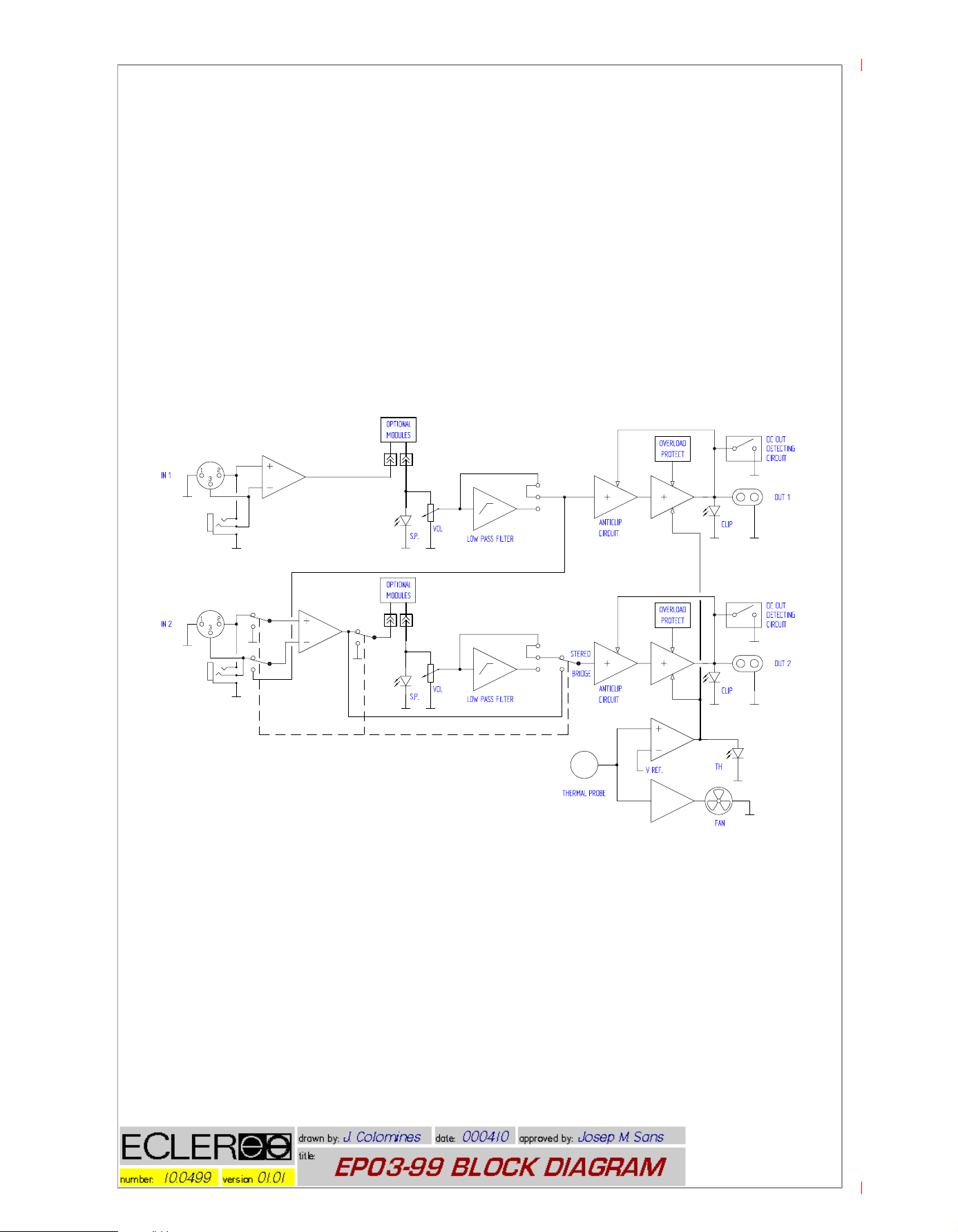

author: Queralt date: 000519
C
E
num:
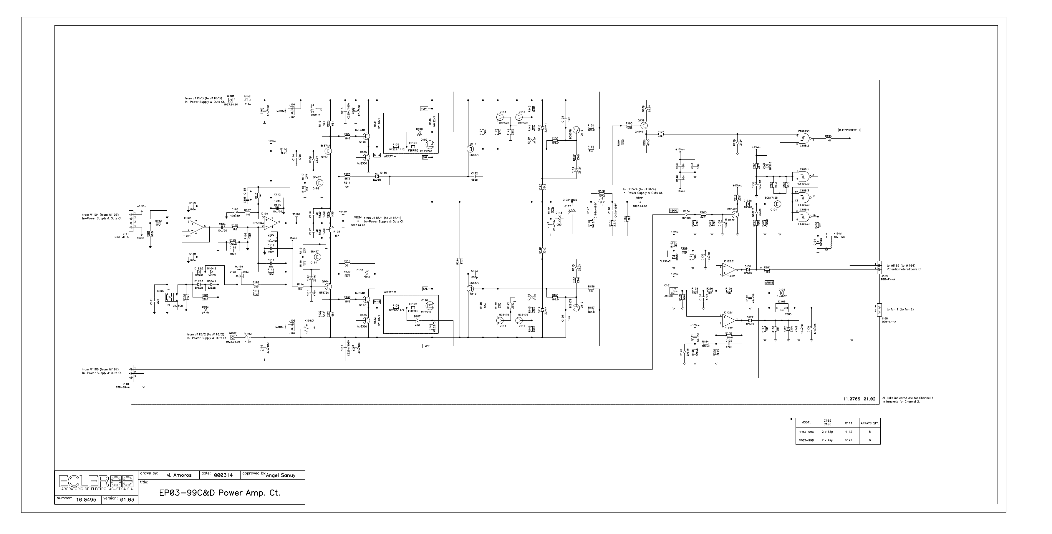
The amplifying stage basic structure is actually the one commonly used until now, this
is, a push-pull mounted A-B class amplifier, using P-type (IRFP9240) and N-type
(IRFP240) mosfets.
The system's controlling core is a NE5534 OpAmp, which is internally compensated in
order to obtain an amplifying gain ratio equal or greater than 3. The amplifier's
feedback runs through a resistor and a capacitor associated to the OpAmp's noninverting input.
Transistors BF871 and BF872 are common-base configured, becoming actually a
current source structure. They accomplish a dual function: on one hand, they polarise
the mosfet's gate-source junction, keeping them on their conduction knee. On the other
hand, they carry out the OpAmp's output voltage variations, referred to signal ground.
The polarisation current adjustment is fixed by a 2k5 trimming potentiometer connected
to the BF transistors base. This current is added to the current source's output, which
passes through the BF-transistors load resistors. The bias current stability against
temperature is fixed through the BD437 transistors. Their temperature- dependent base
emitter voltage curve is used to alter adequately the current source's reference voltage.
As a consequence, if the temperature rises, the reference voltage decreases, thus the
gate-source voltage also does, and finally the bias current also decreases.
LER
52.0007 version: 01.00
approved:
title:
FUNCTIONING DESCRIPTION
POWER MODULE
The Zobel network, formed by a resistor-inductor-capacitor group, and which is located
at the amplifier's output, intends to keep the amplifier's load impedance as constant as
possible, no matter which load is connected to the stage's output, or which signal
frequency is to be amplified, in order to prevent an inverted-phase feedback signal.
In order to avoid a DC offset on the output signal, a diac-triac tandem system is used,
which shorts the output to signal ground when the DC level is enough to get the diac
triggered. To prevent this from happening while carrying audio signal (sine-wave,
music), the diac's reference voltage is taken from a filter formed by resistor R149 and
capacitor C124.
The protection circuitry supervises at any time the power consumed by the MOSFETS.
The circuitry basically consists on two sections: MOSFET's drain current (Id) monitoring
and drain-source voltage (Vds) monitoring.
When the drain current exceeds a certain limiting value, a transistor (called controltransistor) becomes conducting, together with an auxiliary circuitry (helper), formed by
a transistor (which is the same type as the control-transistor) and a 8'2V Zener diode.
This value determines the point where the auxillary circuitry starts to run. The helpertransistor's base-emitter junction curve is used to obtain a non-linear variation on the
MOSFETS gate-source voltage control, and thus on their drain current.
Sheet 1 of 2

author: Queralt date: 000519
C
E
num:
Moreover, as the helper-transistor's base-emitter current is temperature-dependent, the
controlling circuitry (basically the control-transistor) compensates the safe operation
area (SOA) drift due to temperature.
If the MOSFET's drain-source voltage (Vds) drops too low, a second circuitry actuates
to alter the control-transistor's triggering level, obtaining a SOA-like curve section and
a current stage, which can be adjusted adequately in order to maintain the MOSFET's
power consumption as close as possible to its SOA.
Moreover, the amplifier also includes an ANTICLIP system.
When the amplifier reaches its clipping level, the OpAmp becomes unable to keep the
system under control, and as a consequence ±V peaks appear at its output (15V
power supply). This peaks are used to be rectified and sent to an optocupler (ledresistor) which modifies its impedance as a function of those peaks' amplitude. The
resulting impedance is part of a voltage divider, together with the amplifier's input
impedance. So, as the optocoupler increases its impedance, the amplifier's input signal
level decreases until the system becomes stable.
LER
52.0007 version: 01.00
approved:
title:
FUNCTIONING DESCRIPTION
POWER MODULE
Also a dual-function temperature control circuitry is provided:
- Temperature-depending control of the cooling fan speed, whose voltage supply is
variable between 7 and 14 Vac.
- Amplifier shutdown when temperature exceeds approximately 90ºC.
The circuitry is formed by LM35D-type IC, which acts like a thermal probe, an
amplifier, thermal probe level comparator and a 7805-type voltage regulator.
The amplifier is responsible for the cooling fan speed control. The comparator triggers a
relay, which cuts off the MOSFETs' bias current by shunting a 22W resistance to the
BF-type transistors' load resistors. This way, the output signal of the amplifier is
effectively cutted off.
The STAND-BY circuit.
This circuit keeps the safety relay closed for about 10 seconds, thus the MOSFET's
bias current is cutted off during this period, until the whole system reaches again a
voltage-stable situation. Due to this, hearing annoying transients and noises during start
up through the loudspeakers is avoided. This delay is obtained by a RC-cell, where
R=287K, and C=47µF/50V. During start up, this RC-cell's voltage smoothly rises until
the 40106-type Trigger-Schmitt trigging level is reached, and the amplifier starts
functioning. C=47µF resets or discharges when the unit is turned off. During a short
period of time, a BC817-type transistor acts like a switch, connecting two 75W parallel
resistors to C=47µ/50V.
Sheet 2 of 2

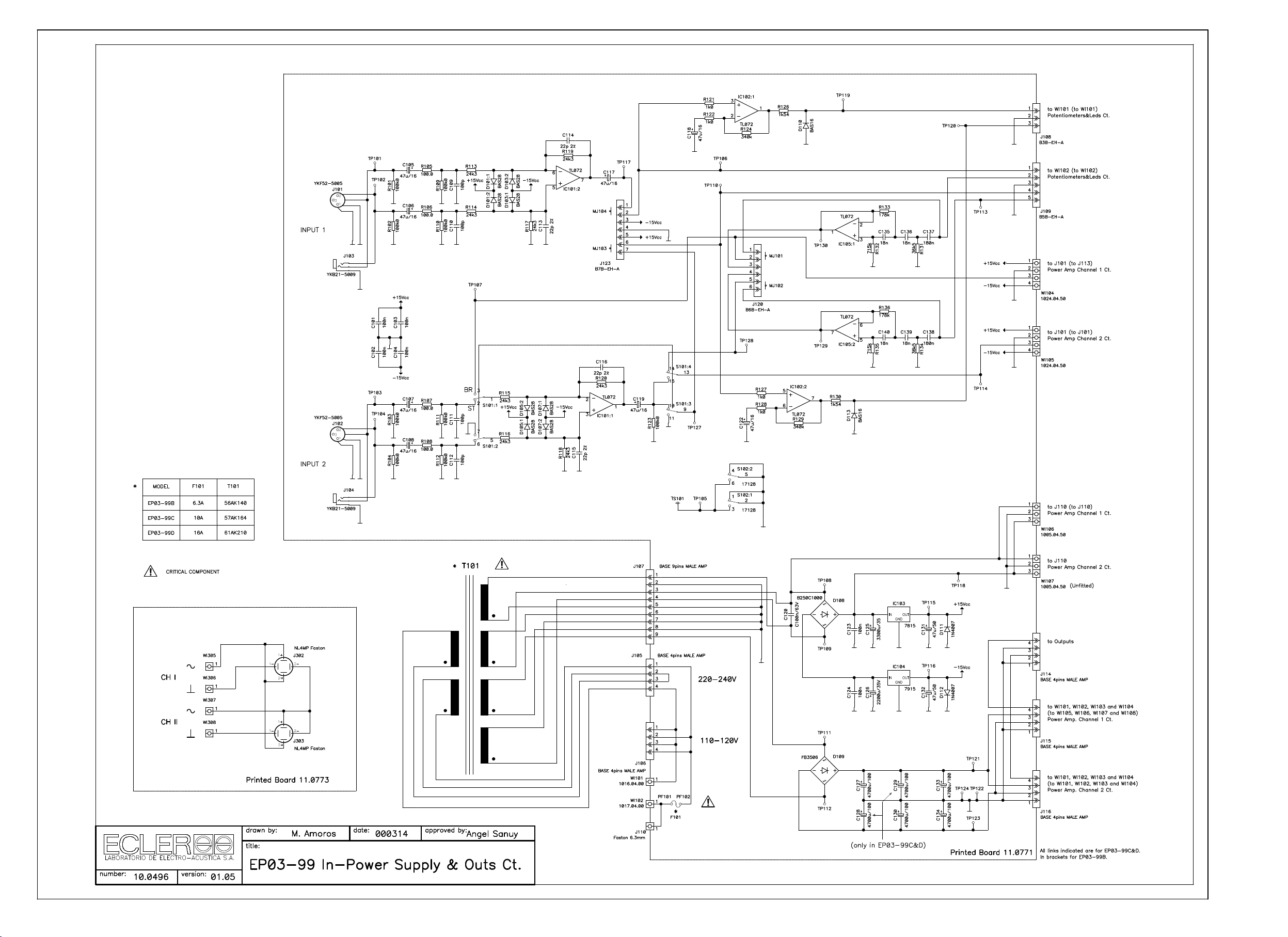
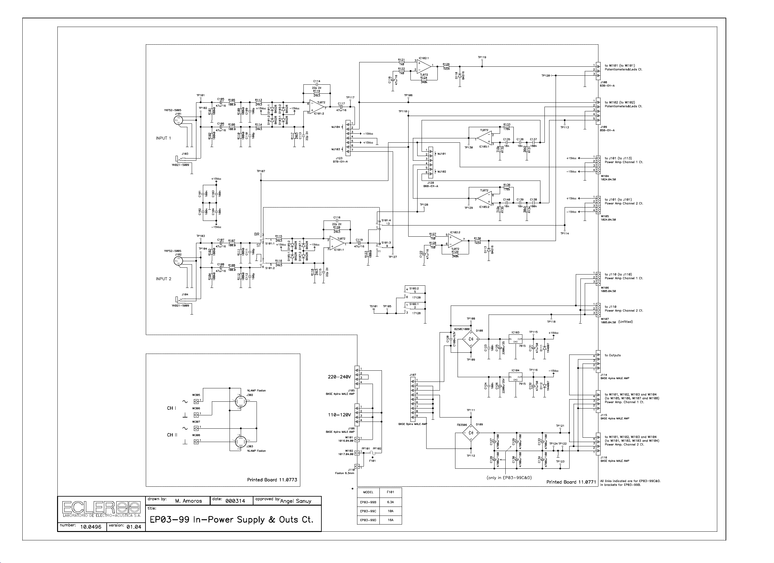

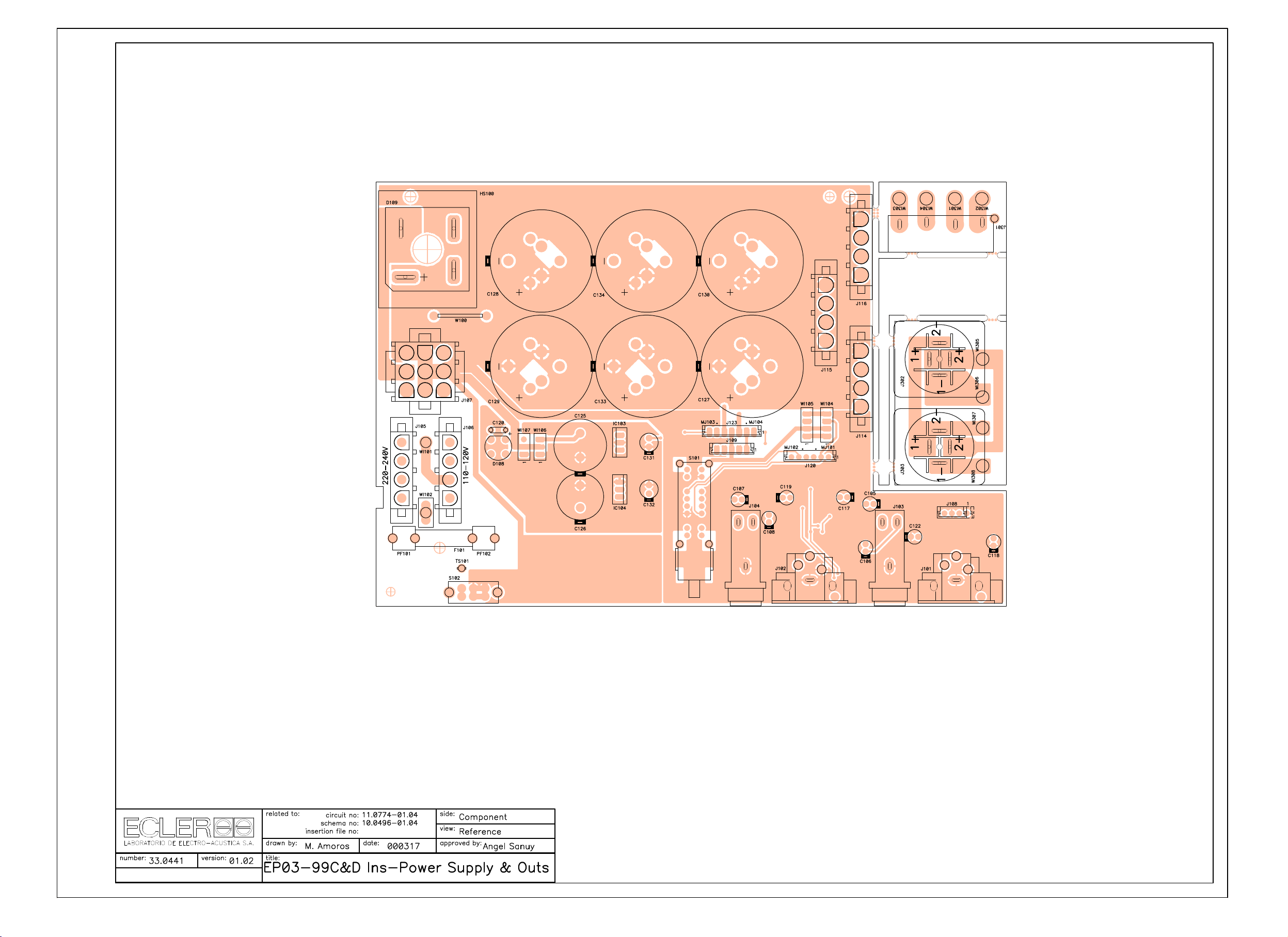
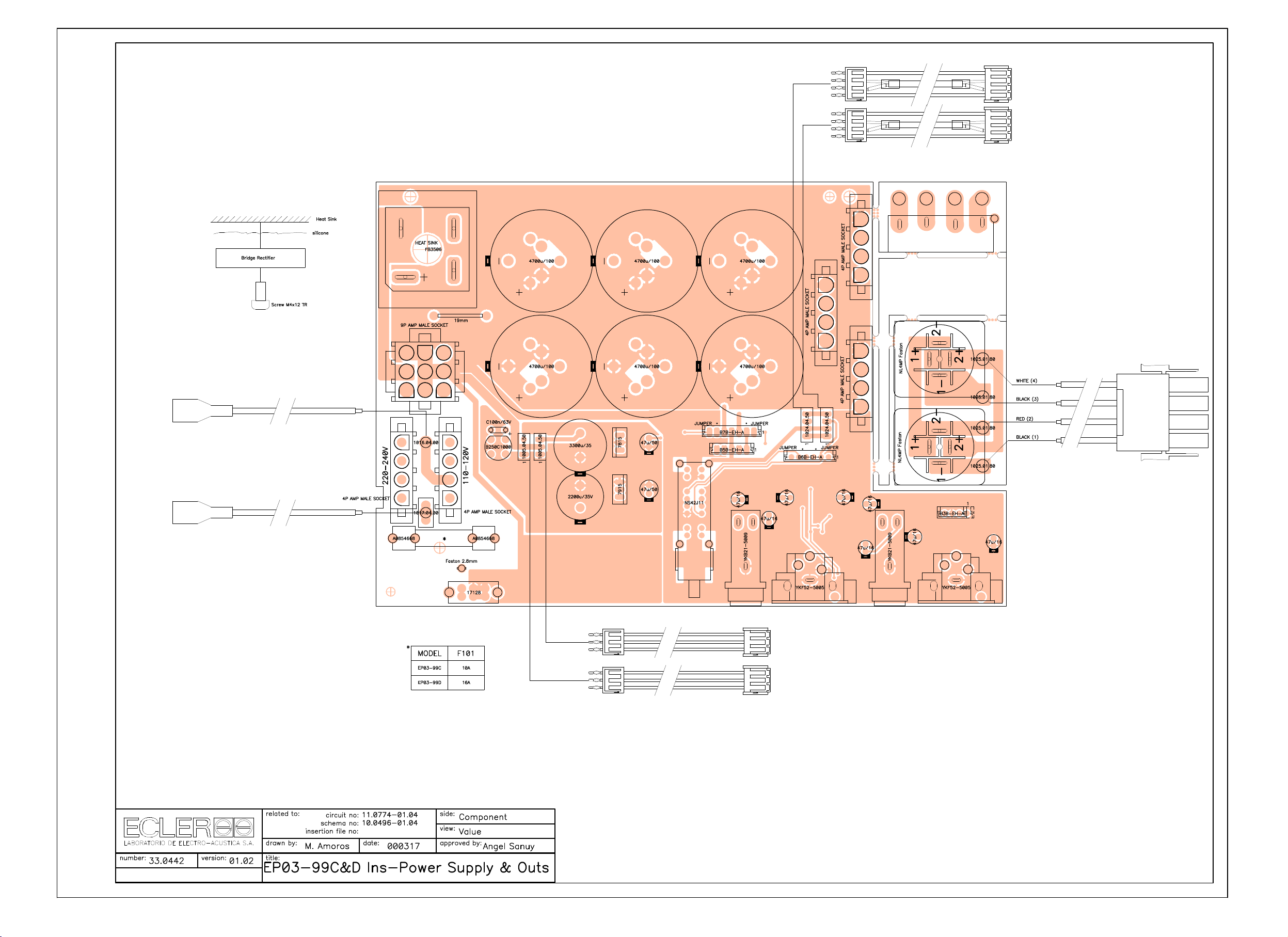

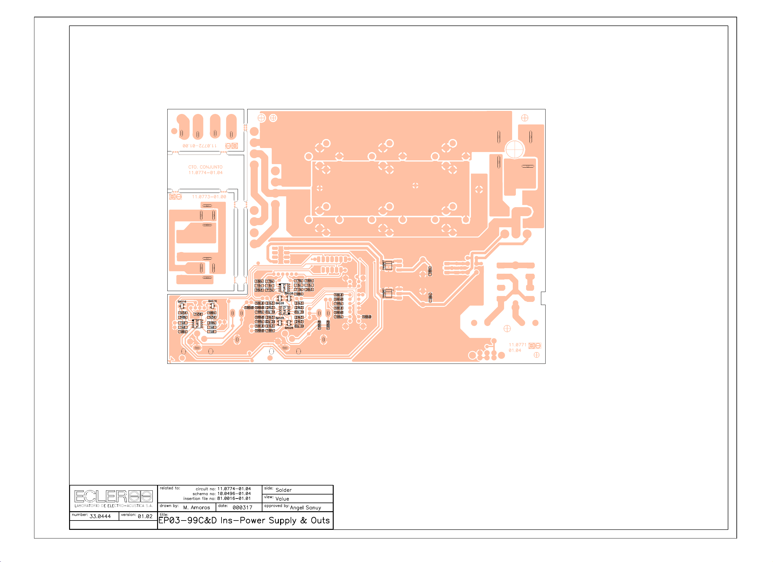

author: Queralt date: 020430
C
E
num:
REFERENCE VALUE CODE
C101 100n FCXCN41000
C102 100n FCXCN41000
C103 100n FCXCN41000
C104 100n FCXCN41000
C105 47u/16 FCCE100000
C106 47u/16 FCCE100000
C107 47u/16 FCCE100000
C108 47u/16 FCCE100000
C109 100p FCXCN21000
C110 100p FCXCN21000
C111 100p FCXCN21000
C112 100p FCXCN21000
C113 22p 2% FCXCN12201
C114 22p 2% FCXCN12201
C115 22p 2% FCXCN12201
C116 22p 2% FCXCN12201
C117 47u/16 FCCE100000
C118 47u/16 FCCE100000
C119 47u/16 FCCE100000
C120 C100n/63V FCCDK11000
C122 47u/16 FCCE100000
C123 100n FCXCN41000
C124 100n FCXCN41000
C125 3300u/35 FCCE213300
C126 2200u/35V FCCE212200
C127 4700u/100 FCCE331525
C128 4700u/100 FCCE331525
C129 4700u/100 FCCE331525
C130 4700u/100 FCCE331525
C131 47u/50 FCCE250470
C132 47u/50 FCCE250470
C133 4700u/100 FCCE331525
C134 4700u/100 FCCE331525
C135 18n FCXCN40180
C136 18n FCXCN40180
C137 180n FCXCN41800
C138 180n FCXCN41800
C139 18n FCXCN40180
C140 18n FCXCN40180
D101 BAS28 FCXDDBAS28
D103 BAS28 FCXDDBAS28
D105 BAS28 FCXDDBAS28
D107 BAS28 FCXDDBAS28
D108 B250C1000 FCREC25100
D109 FB3506 FCREC35060
D110 BAS16 FCXDDBAS16
D111 1N4007 FCXDD40070
D112 1N4007 FCXDD40070
D113 BAS16 FCXDDBAS16
F101 FOR 230V T10A FCFUS60100
F101 FOR 115V T16A FCFUS60400
HS100 HEAT SINK FCRAD11515
40-0048-0101 EP03-99c&d.xls SHEET 1 OF 3
LER
40.0048 version: 01.01
approved:
model:
EP03-99C&D
PRINTED CIRCUIT 11.0774-01.04
PARTS LIST

PRINTED CIRCUIT 11.0774-01.04
REFERENCE VALUE CODE
IC101 TL072 FCIC072010
IC102 TL072 FCIC072010
IC103 7815 FCREG78150
IC104 7915 FCREG79150
IC105 TL072 FCIC072010
J101 YKF52-5005 FCBASX0900
J102 YKF52-5005 FCBASX0900
J103 YKB21-5009 FCBASJ0200
J104 YKB21-5009 FCBASJ0200
J105 BASE 4pins MALE FCCTAMP040
J106 BASE 4pins MALE FCCTAMP040
J107 BASE 9pins MALE FCCTAMP090
J108 B3B-EH-A FCCTM00030
J109 B5B-EH-A FCCTM00050
J110 FASTON 6.3mm FCTERMF630
J114 BASE 4pins MALE FCCTAMP040
J115 BASE 4pins MALE FCCTAMP040
J116 BASE 4pins MALE FCCTAMP040
J120 B6B-EH-A FCCTM00060
J123 B7B-EH-A FCCTM00070
J302 NL4MP Faston FCBASS0100
J303 NL4MP Faston FCBASS0100
MJ101 JUMPER FCMJ000100
MJ102 JUMPER FCMJ000100
MJ103 JUMPER FCMJ000100
MJ104 JUMPER FCMJ000100
PF101 A0854668 FCPORF0100
PF102 A0854668 FCPORF0100
R101 100k0 FCXR151000
R102 100k0 FCXR151000
R103 100k0 FCXR151000
R104 100k0 FCXR151000
R105 100.0Ω FCXR121000
R106 100.0Ω FCXR121000
R107 100.0Ω FCXR121000
R108 100.0Ω FCXR121000
R109 100k0 FCXR151000
R110 100k0 FCXR151000
R111 100k0 FCXR151000
R112 100k0 FCXR151000
R113 24k3 FCXR242430
R114 24k3 FCXR242430
R115 24k3 FCXR242430
R116 24k3 FCXR242430
R117 24k3 FCXR242430
R118 24k3 FCXR242430
R119 24k3 FCXR242430
R120 24k3 FCXR242430
R121 1k0 FCXR131000
R122 1k0 FCXR131000
R123 100k0 FCXR151000
R124 340k FCXR153400
R126 1k54 FCXR131540
R127 1k0 FCXR131000
R128 1k0 FCXR131000
R129 340k FCXR153400
R130 1k54 FCXR131540
R131 36k5 FCXR143650
40-0048-0101 EP03-99c&d.xls SHEET 2 OF 3

PRINTED CIRCUIT 11.0774-01.04
REFERENCE VALUE CODE
R132 715k FCXR157150
R133 178k FCXR151780
R134 36k5 FCXR143650
R135 715k FCXR157150
R136 178k FCXR151780
R137 1k50 FCXR131500
S101 NS42J11 FCINTAP080
S102 17128 FCINTD4000
SC100 M4x12 TR FCT3804012
TS101 T-120 FCTERMF280
W100 19mm FCMECPON19
WI101 1016.04.00 FC2F016400
WI102 1017.04.00 FC2F017400
WI104 1024.04.50 FC6J024450
WI105 1024.04.50 FC6J024450
WI106 1005.04.50 FC4I005450
WI107 1005.04.50 FC4I005450
WI305 1025.01.80 FC0H025180
WI306 1025.01.80 FC0H025180
WI307 1025.01.80 FC0H025180
WI308 1025.01.80 FC0H025180
40-0048-0101 EP03-99c&d.xls SHEET 3 OF 3


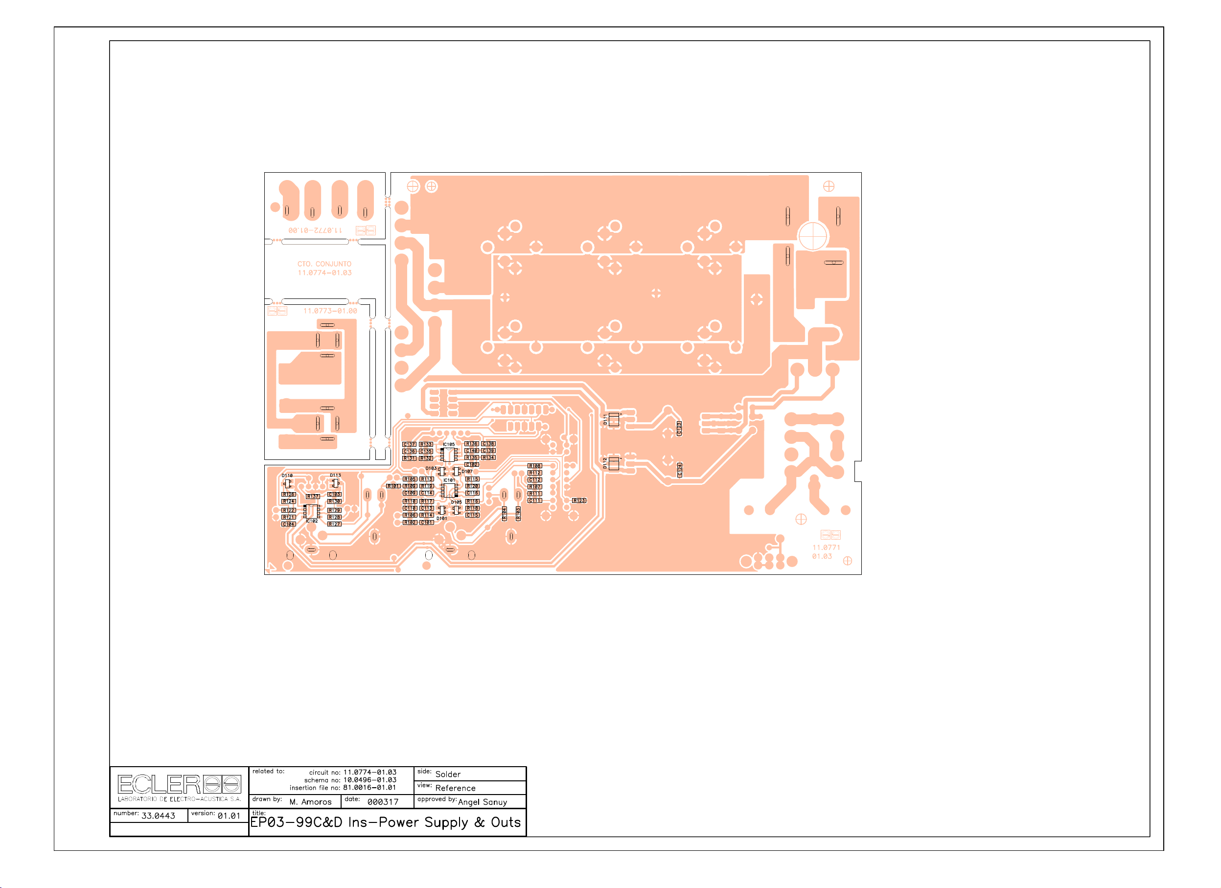


author: Queralt date: 000913
C
E
num:
REFERENCE VALUE CODE
C101 100n FCXCN41000
C102 100n FCXCN41000
C103 100n FCXCN41000
C104 100n FCXCN41000
C105 47u/16 FCCE100000
C106 47u/16 FCCE100000
C107 47u/16 FCCE100000
C108 47u/16 FCCE100000
C109 100p FCXCN21000
C110 100p FCXCN21000
C111 100p FCXCN21000
C112 100p FCXCN21000
C113 22p 2% FCXCN12201
C114 22p 2% FCXCN12201
C115 22p 2% FCXCN12201
C116 22p 2% FCXCN12201
C117 47u/16 FCCE100000
C118 47u/16 FCCE100000
C119 47u/16 FCCE100000
C120 C100n/63V FCCDK11000
C122 47u/16 FCCE100000
C123 100n FCXCN41000
C124 100n FCXCN41000
C125 3300u/35 FCCE213300
C126 2200u/35V FCCE212200
C127 4700u/100 FCCE331525
C128 4700u/100 FCCE331525
C129 4700u/100 FCCE331525
C130 4700u/100 FCCE331525
C131 47u/50 FCCE250470
C132 47u/50 FCCE250470
C133 4700u/100 FCCE331525
C134 4700u/100 FCCE331525
C135 18n FCXCN40180
C136 18n FCXCN40180
C137 180n FCXCN41800
C138 180n FCXCN41800
C139 18n FCXCN40180
C140 18n FCXCN40180
D101 BAS28 FCXDDBAS28
D103 BAS28 FCXDDBAS28
D105 BAS28 FCXDDBAS28
D107 BAS28 FCXDDBAS28
D108 B250C1000 FCREC25100
D109 FB3506 FCREC35060
D110 BAS16 FCXDDBAS16
D111 1N4007 FCXDD40070
D112 1N4007 FCXDD40070
D113 BAS16 FCXDDBAS16
F101 FOR 230V T10A FCFUS60100
F101 FOR 115V T16A FCFUS60400
HS100 HEAT SINK FCRAD11515
40-0048-0100 EP03-99c&d.xls SHEET 1 OF 3
LER
40.0048 version: 01.00
approved:
model:
EP03-99C&D
PRINTED CIRCUIT 11.0774-01.03
PARTS LIST

PRINTED CIRCUIT 11.0774-01.03
REFERENCE VALUE CODE
IC101 TL072 FCIC072010
IC102 TL072 FCIC072010
IC103 7815 FCREG78150
IC104 7915 FCREG79150
IC105 TL072 FCIC072010
J101 YKF52-5005 FCBASX0900
J102 YKF52-5005 FCBASX0900
J103 YKB21-5009 FCBASJ0200
J104 YKB21-5009 FCBASJ0200
J105 BASE 4pins MALE FCCTAMP040
J106 BASE 4pins MALE FCCTAMP040
J107 BASE 9pins MALE FCCTAMP090
J108 B3B-EH-A FCCTM00030
J109 B5B-EH-A FCCTM00050
J110 FASTON 6.3mm FCTERMF630
J114 BASE 4pins MALE FCCTAMP040
J115 BASE 4pins MALE FCCTAMP040
J116 BASE 4pins MALE FCCTAMP040
J120 B6B-EH-A FCCTM00060
J123 B7B-EH-A FCCTM00070
J302 NL4MP Faston FCBASS0100
J303 NL4MP Faston FCBASS0100
MJ101 JUMPER FCMJ000100
MJ102 JUMPER FCMJ000100
MJ103 JUMPER FCMJ000100
MJ104 JUMPER FCMJ000100
PF101 A0854668 FCPORF0100
PF102 A0854668 FCPORF0100
R101 100k0 FCXR151000
R102 100k0 FCXR151000
R103 100k0 FCXR151000
R104 100k0 FCXR151000
R105 100.0Ω FCXR121000
R106 100.0Ω FCXR121000
R107 100.0Ω FCXR121000
R108 100.0Ω FCXR121000
R109 100k0 FCXR151000
R110 100k0 FCXR151000
R111 100k0 FCXR151000
R112 100k0 FCXR151000
R113 24k3 FCXR242430
R114 24k3 FCXR242430
R115 24k3 FCXR242430
R116 24k3 FCXR242430
R117 24k3 FCXR242430
R118 24k3 FCXR242430
R119 24k3 FCXR242430
R120 24k3 FCXR242430
R121 1k0 FCXR131000
R122 1k0 FCXR131000
R123 100k0 FCXR151000
R124 340k FCXR153400
R126 1k54 FCXR131540
R127 1k0 FCXR131000
R128 1k0 FCXR131000
R129 340k FCXR153400
R130 1k54 FCXR131540
R131 36k5 FCXR143650
40-0048-0100 EP03-99c&d.xls SHEET 2 OF 3

PRINTED CIRCUIT 11.0774-01.03
REFERENCE VALUE CODE
R132 715k FCXR157150
R133 178k FCXR151780
R134 36k5 FCXR143650
R135 715k FCXR157150
R136 178k FCXR151780
R137 1k50 FCXR131500
S101 NS42J11 FCINTAP080
S102 17128 FCINTD4000
SC100 M4x12 TR FCT3804012
TS101 IB.311 FCTERMSOL0
W100 19mm FCMECPON19
WI101 1016.04.00 FC2F016400
WI102 1017.04.00 FC2F017400
WI104 1024.04.50 FC6J024450
WI105 1024.04.50 FC6J024450
WI106 1005.04.50 FC4I005450
WI107 1005.04.50 FC4I005450
WI305 1025.01.80 FC0H025180
WI306 1025.01.80 FC0H025180
WI307 1025.01.80 FC0H025180
WI308 1025.01.80 FC0H025180
40-0048-0100 EP03-99c&d.xls SHEET 3 OF 3

ECL ER
51.0078
num:
version:
01.00
author:
approved:
J. Colomines
date:
title:
020426
project:
product:
TECHNICAL BRIEFING
Announcement addressed to Technical Support Services
Involved series:
APA1400 / APA1000 / APA600
PAM1100 / PAM2100
MPA4-80 / MPA6-80 / MPA4-150
VOLUME potentiometer replacement.
Replaced service part code: FCPR210040
When this potentiometer is being replaced, after soldering it on the printed circuit
board, the two leads should be shorted as shown in the picture, in order to ensure a
correct performance depending on the available service part.
POWER AMPLIFIERS
51-0078-0100 Potenciòmetre etapes.doc 1 of 1

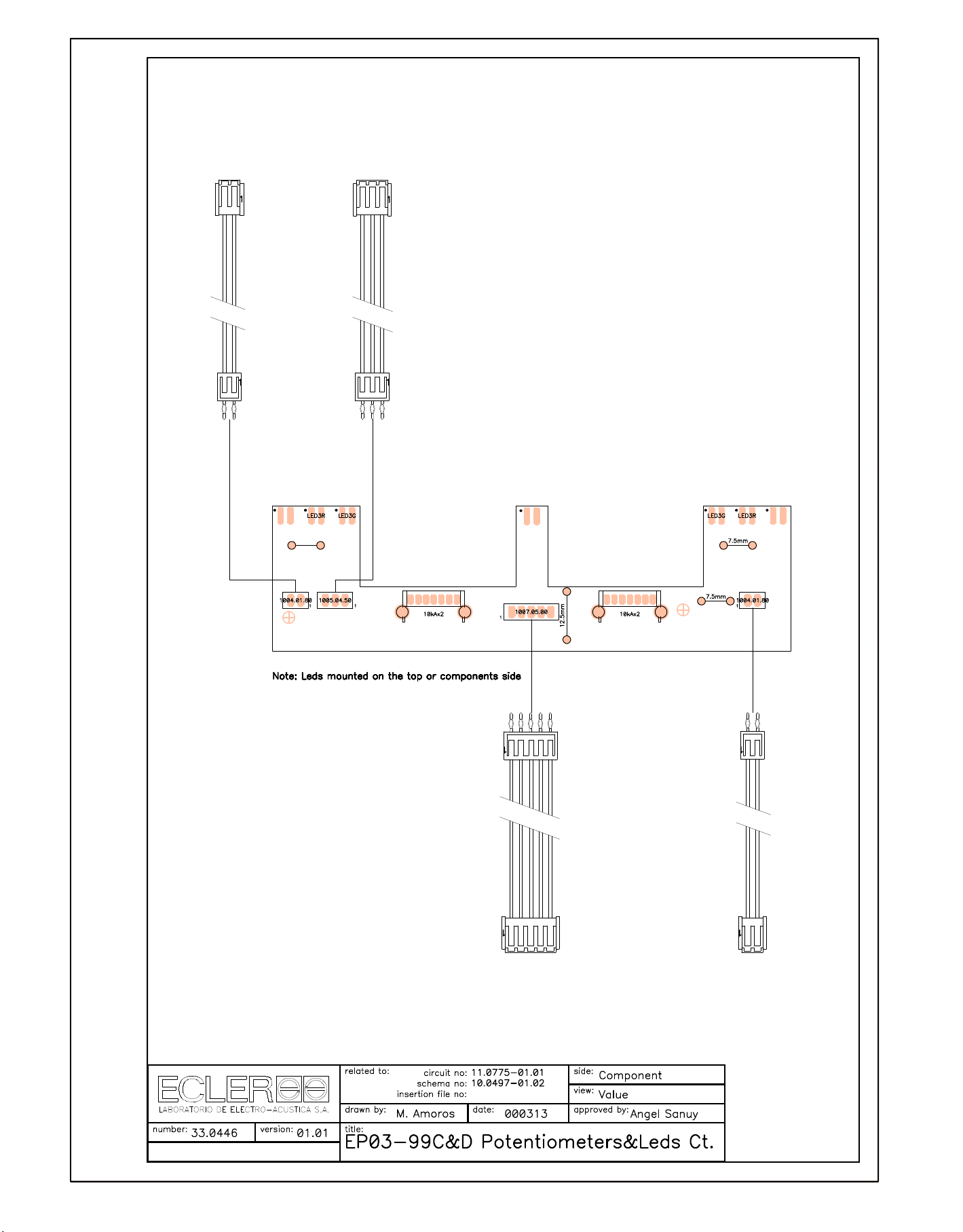

author: Queralt date: 000913
C
E
num:
REFERENCE VALUE CODE
D101 LED3G FCLED300VE
D102 LED3G FCLED300VE
D103 LED3R FCLED300RO
D104 LED3Y FCLED300AM
D105 LED3R FCLED300RO
D106 LED3Y FCLED300AM
D107 UNFITTED FCLED300AM
R101 10kAx2 FCPR210040
R102 10kAx2 FCPR210040
W100 7.5mm FCPONT0075
W101 12.5mm FCPONT0125
W102 7.5mm FCPONT0075
W103 7.5mm FCPONT0075
WI101 1005.04.50 FC4I005450
WI102 1007.05.00 FC4K007500
WI103 1004.01.80 FC4G004180
WI104 1004.01.80 FC4G004180
LER
40.0049 version: 01.00
approved:
model:
EP03-99C&D
PRINTED CIRCUIT 11.0775-01.01
PARTS LIST
40-0049-0100 EP03-99c&d.xls SHEET 1 OF 1
 Loading...