

Page 1

®
FT 3120®/ FT 3150
Smart Transceiver Data Book
@®
005-0139-01D
Page 2

Echelon, LON, LONWORKS, Neuron, 3120, 3150, LonTalk, NodeBuilder, LNS,
LonMaker, i.LON, and the Echelon logo are trademarks of Echelon Corporation
registered in the United States and other countries.
Other brand and product names are trademarks or registered trademarks of their
respective holders.
Smart Transceivers, Neuron Chips, and other OEM Products were not designed
for use in equipment or systems which involve danger to human health or safety
or a risk of property damage and Echelon assumes no responsibility or liability
for use of the Smart Transceivers or Neuron Chips in such applications.
Parts manufactured by vendors other than Echelon and referenced in this
document have been described for illustrative purposes only, and may not have
been tested by Echelon. It is the responsibility of the customer to determine the
suitability of these parts for each application
ECHELON MAKES AND YOU RECEIVE NO WARRANTIES OR
CONDITIONS, EXPRESS, IMPLIED, STATUTORY OR IN ANY
COMMUNICATION WITH YOU, AND ECHELON SPECIFICALLY
DISCLAIMS ANY IMPLIED WARRANTY OF MERCHANTABILITY OR
FITNESS FOR A PARTICULAR PURPOSE.
No part of this publication may be reproduced, stored in a retrieval system, or
transmitted, in any form or by any means, electronic, mechanical, photocopying,
recording, or otherwise, without the prior written permission of Echelon
Corporation.
.
Printed in the United States of America.
Copyright ©2002-2006 by Echelon Corporation.
Echelon Corporation
www.echelon.com
Page 3

Table of Contents
Chapter 1 - Introduction ......................................................................................1
Introduction .......................................................................................................2
Audience ...........................................................................................................2
Product Overview .............................................................................................2
Free Topology Technology Overview ..............................................................4
Related Documentation .....................................................................................5
Chapter 2 - Hardware Resources ........................................................................7
Overview ...........................................................................................................8
Neuron Processor Architecture .........................................................................8
Memory Allocation .........................................................................................13
FT 3120 Smart Transceiver ......................................................................13
FT 3150 Smart Transceiver ......................................................................13
EEPROM ..................................................................................................14
Static RAM ...............................................................................................16
Preprogrammed ROM ...............................................................................16
External Memory of the FT 3150 Smart Transceiver ...............................16
Input/Output ...................................................................................................17
Eleven Bidirectional I/O Pins ...................................................................17
Two 16-Bit Timer/Counters ......................................................................17
Clock Input .....................................................................................................18
Clock Generation ......................................................................................18
Additional Functions .......................................................................................19
Reset Function ..........................................................................................19
RESET Pin ................................................................................................20
Power Up Sequence ............................................................................20
Software Controlled Reset ..................................................................21
Watchdog Timer .................................................................................21
LVI Considerations .............................................................................21
Reset Processes and Timing .....................................................................22
SERVICE
Integrity Mechanisms .....................................................................................28
Memory Integrity Using Checksums ........................................................28
Reboot and Integrity Options Word ..........................................................29
Reset Processing .......................................................................................30
Signatures ..................................................................................................30
Pin ...........................................................................................27
Chapter 3 - Input/Output Interfaces ................................................................31
Overview .........................................................................................................32
Hardware Considerations ................................................................................33
I/O Timing Issues ............................................................................................37
Scheduler-Related I/O Timing Information ..............................................38
Firmware and Hardware-Related I/O Timing Information .......................39
FT 3120 / 3150 Smart Tranceiver Data Book i
Page 4

Table of Contents
Direct I/O Objects ..........................................................................................40
Bit Input/Output ........................................................................................40
Byte Input/Output .....................................................................................41
Leveldetect Input ......................................................................................43
Nibble Input/Output ..................................................................................44
Parallel I/O Objects ........................................................................................45
Muxbus Input/Output ................................................................................45
Parallel Input/Output .................................................................................46
Master/Slave A Mode .........................................................................47
Slave B Mode ......................................................................................51
Token Passing .....................................................................................52
Handshaking .......................................................................................53
Data Transferring ................................................................................54
Serial I/O Objects ...........................................................................................57
Bitshift Input/Output .................................................................................57
I2C Input/Output .......................................................................................59
Magcard Input ...........................................................................................60
Magtrack1 Input ........................................................................................62
Neurowire (SPI Interface) Input/Output Object .......................................63
Neurowire Master Mode .....................................................................63
Neurowire Slave Mode .......................................................................64
Serial Input/Output ...................................................................................66
Touch Input/Output ...................................................................................67
Wiegand Input ...........................................................................................69
Timer/Counter Input Objects ..........................................................................70
Dualslope Input .........................................................................................71
Edgelog Input ............................................................................................72
Infrared Input ............................................................................................73
Ontime Input .............................................................................................74
Period Input ...............................................................................................75
Pulsecount Input .......................................................................................77
Quadrature Input .......................................................................................78
Totalcount Input ........................................................................................79
Timer/Counter Output Objects .......................................................................80
Edgedivide Output ....................................................................................80
Frequency Output .....................................................................................81
Oneshot Output .........................................................................................83
Pulsecount Output .....................................................................................84
Pulsewidth Output .....................................................................................85
Triac Output ..............................................................................................86
Triggered Count Output ............................................................................87
Notes ..............................................................................................................88
ii FT 3120 / 3150 Smart Tranceiver Data Book
Page 5

Chapter 4 - Hardware Design Considerations .................................................91
Introduction .....................................................................................................92
Quick Start for Users Familiar With The FTT-10A Transceiver ...................92
Interface Between Smart Transceivers and the Network ................................93
PC Board Layout Guidelines ..........................................................................95
EMI Design Issues ..........................................................................................98
ESD Design Issues ........................................................................................101
Lightening Protection ...................................................................................102
Building Entrance Protection ..................................................................102
Network Line Protection .........................................................................102
Shield Protection .....................................................................................103
Suggested Gas Discharge Arresters ........................................................103
EN 61000-4 Electromagnetic Compatibility (EMC) Testing .......................104
Chapter 5 - Network Cabling and Connections .............................................109
Network Connection .....................................................................................110
Network Topology Overview .......................................................................110
System Performance and Cable Selection ....................................................111
System Specifications .............................................................................112
Transmission Specifications ...................................................................112
Cable Termination and Shield Grounding ....................................................113
Free Topology Network Segment ...........................................................113
Doubly Terminated Bus Topology Segment ..........................................113
Grounding Shielded Twisted Pair Cable ................................................114
Chapter 6 - Programming Considerations .....................................................115
Application Program Development and Export ............................................116
LonBuilder Developers Kit ...........................................................................116
Development Hardware Setup ................................................................116
Release Hardware Setup .........................................................................118
NodeBuilder Development Tool ...................................................................118
Development Hardware Setup ................................................................118
Release Hardware Setup .........................................................................119
Appendix A - FT Smart Transceiver Design Checklist .................................121
Introduction ...................................................................................................122
Device Checklist ...........................................................................................122
Appendix B - Qualified TP/FT-10 Cable Specifications and Sources ..........125
Introduction ...................................................................................................126
Qualified Cables ...........................................................................................126
Category 5 Cable Specifications .............................................................126
NEMA Level IV Cable Specifications ...................................................126
16AWG/1.3mm “Generic” Cable Specifications ...................................128
FT 3120 / 3150 Smart Tranceiver Data Book iii
Page 6

Table of Contents
Appendix C - Design and Handling Guidelines .............................................129
Application Considerations ...........................................................................130
Termination of Unused Pins ...................................................................130
Avoidance of Damaging Conditions .......................................................130
Power Supply, Ground, and Noise Considerations .................................132
Decoupling Capacitors ............................................................................133
Board Soldering Considerations ...................................................................134
Soldering Through-hole Parts (FT-X1) ..................................................134
Soldering Surface Mount (SMT) Parts (Free Topology Transceivers) ..135
Handling Precautions and Electrostatic Discharge .......................................135
Electrostatic Discharge ...........................................................................138
Recommended Reading ..........................................................................139
Power Distribution and Decoupling Capacitors ...........................................139
Recommended Bypass Capacitor Placement ................................................140
Appendix D - Reference Design Schematics and Layout ...............................141
Mini Evaluation Kit Board ............................................................................142
FT 3150 Evaluatin Board Core......................................................................143
FT 3150 Evaluation Board Peripheral Circuitry............................................144
FT 3150 Evaluation Board Composite Top Layer.........................................145
FT 3150 Evaluation Board Top Layer...........................................................146
FT 3150 Evaluation Board Internal Ground Layer........................................147
FT 3150 Evaluation Board Internal Power Layer..........................................148
FT 3150 Evaluation Board Bottom Layer .....................................................149
FT 3150 Evaluation Board Composite Bottom Layer ...................................150
iv FT 3120 / 3150 Smart Tranceiver Data Book
Page 7

1
Introduction
FT 3120 / FT 3150 Smart Transceiver Data Book 1
Page 8

Chapter 1 - Introduction
Introduction
This manual provides detailed technical specifications on the electrical interfaces, mechanical interfaces, and
®
operating environment characteristics for the FT 3120
guidelines for migrating applications to an FT Smart Transceiver-based device using a LonBuilder
®
NodeBuilder
In some cases, vendor sources are included in this manual to simplify the task of integrating FT Smart Transceivers
with application electronics.
There is a list of related documentation at the end of this chapter in the section Related Documentation. The
documents listed in that section can be found on the Echelon website (www.echelon.com) unless otherwise noted.
development tool.
and FT 3150® Smart Transceivers. This manual also provides
®
or
Audience
This manual provides specifications and user instructions for FT Smart Transceiver customers, and users of network
interfaces based on the FT Smart Transceivers.
Product Overview
The FT Smart Transceivers integrate a Neuron® 3120 or Neuron 3150 network processor core, respectively, with a
free topology (FT) twisted-pair transceiver to create a low cost, smart transceiver on a chip. Combined with the
Echelon high performance FT-X1 or FT-X2 Communication Transformer, the FT Smart Transceivers set new
benchmarks for performance, robustness, and low cost. Ideal for use in L
industrial, transportation, home, and utility automation applications, the FT Smart Transceivers can be used in both
new product designs and as a means of cost reducing existing devices.
ONWORKS
®
devices designed for building,
The integral transceiver is fully compatible with the TP/FT-10 channel and can communicate with devices using the
Echelon FTT-10A Free Topology Transceiver, and with the addition of suitable DC isolation capacitors, the LPT-10
Link Power Transceiver. The free topology transceiver supports polarity insensitive cabling using a star, bus, daisychain, loop, or combined topologies. This frees the installer from the need to adhere to a strict set of wiring rules. Free
topology wiring reduces the time and expense of device installation by allowing the wiring to be installed in the most
expeditious and cost-effective manner. It also simplifies network expansion by eliminating restrictions on wire
routing, splicing, and device placement.
The FT 3120 Smart Transceiver is a complete system-on-a-chip that is targeted at cost-sensitive and small form factor
designs that require up to 4Kbytes of application code. The Neuron 3120 core operates at up to 40MHz, and includes
4Kbytes of EEPROM and 2Kbytes of RAM. The Neuron firmware is pre-programmed in an on-chip ROM. The
application code is stored in the embedded EEPROM memory and may be updated over the network. The FT 3120
Smart Transceiver is offered in a 32-lead SOIC package as well as a compact 44-lead TQFP package.
The FT 3150 Smart Transceiver includes a 20MHz Neuron 3150 core, 0.5Kbytes of EEPROM and 2Kbytes of RAM.
Through its external memory bus, the FT 3150 Smart Transceiver can address up to 58Kbytes of external memory, of
which 16Kbytes of external non-volatile memory is dedicated to the Neuron system firmware. The FT 3150 Smart
Transceiver is supplied in a 64-lead TQFP package.
The embedded EEPROM may be written up to 10,000 times with no data loss. Data stored in the EEPROM will be
retained for at least 10 years.
Three different versions of the FT Smart Transceivers are available to meet a wide range of applications and
packaging requirements. See the table below for product offerings and descriptions.
2 FT 3120/FT 3150 Smart Transceiver Data Book
Page 9
Product Overview
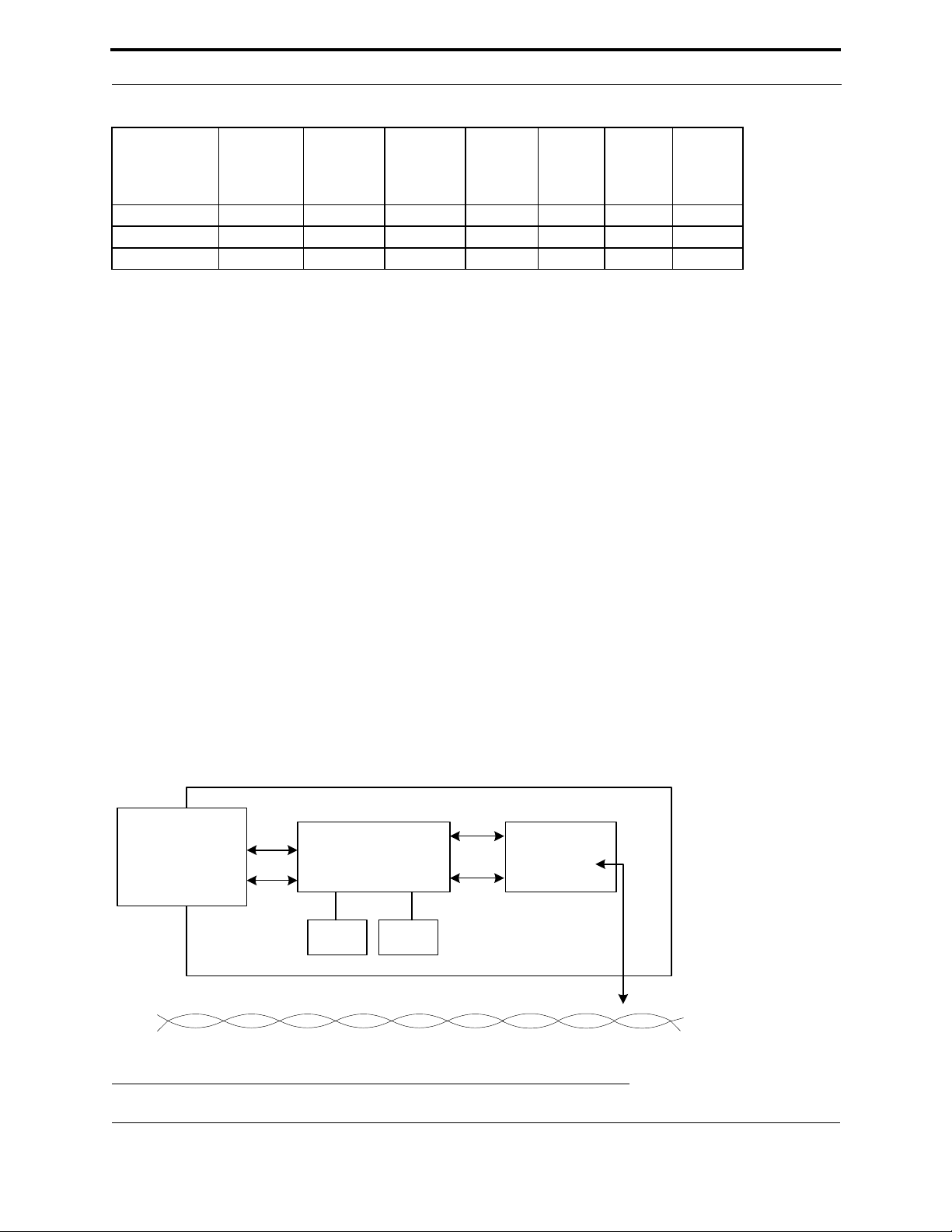
Table 1.1 FT Smart Transceiver Product Offerings
Smart
Transceiver IC
Product
Number
FT 3120-E4S40 14212R-500 40MHz 4Kbytes 2Kbytes 12Kbytes No 32 SOIC
FT 3120-E4P40 14222R-800 40MHz 4Kbytes 2Kbytes 12Kbytes No 44 TQFP
FT 3150-P20 14230R-450 20MHz 0.5Kbytes 2Kbytes N/A Ye s 64 TQFP
Model
Number
Maximum
input clock
EEPROM
(Kbytes)
RAM
(Kbytes)
ROM
(Kbytes)
External
memory
interface
IC
Package
The FT Smart Transceivers provide 11 I/O pins which may be configured to operate in one or more of 34 predefined
standard input/output modes. Combining a wide range of I/O models with two on-board timer/counters enables the
FT Smart Transceivers to interface to application circuits with minimal external logic or software development.
The FT Smart Transceivers can be easily interfaced to other host MCUs by way of the Echelon ShortStack™ or MIP
firmware. When used with the ShortStack or MIP firmware, the FT Smart Transceiver enables any OEM product with
a host microcontroller to quickly and inexpensively become a networked, Internet-accessible device. The ShortStack
firmware uses an SCI or SPI serial interface to communicate between the host and the FT Smart Transceiver. The
MIP firmware uses a high performance parallel or dual-ported RAM interface.
The FT Smart Transceivers are supplied with either an FT-X1or FT-X2 transformer, the patent-pending external
communication transformers. A transformer enables operation in the presence of high frequency common mode noise
on unshielded twisted pair networks. Properly designed devices can meet the rigorous Level 3 requirements of EN
61000-4-6 without the need for a network isolation choke.
The transformer also offers outstanding immunity from magnetic field noise, eliminating the need for protective
magnetic field shields in most applications. The transformer is provided in a potted, 6-pin, through-hole plastic
package.
A typical FT Smart Transceiver-based device requires a power source, crystal, and I/O circuitry. See Figure 1.1 for a
typical FT Smart Transceiver-based device.
The FT Smart Transceivers are compatible withthe Echelon LPT-10 Link Power Transceiver, and they can
communicate with each other on a single twisted pair cable. This capability provides an inexpensive means of
interfacing to devices whose current or voltage requirements would otherwise exceed the capacity of the link power
segment. When equipped with an FT Smart Transceiver and DC blocking capacitors, these devices can be operated
from a local power supply without the need for additional electrical isolation from the link power network.
LONWORKS Device
Sense or Control
Devices, e.g., Motors,
Valves, Encoders,
Lights, Relays,
Switches
Smart Transceiver ICI/O
Crystal
Power
Source
Communication
Transformer
FT-X1 or FT-X2
Data
Rate
of
78
kbps
Free Topology Twisted Pair Network
Figure 1.1 Typical FT Smart Transceiver-based Device
FT 3120/FT 3150 Smart Transceiver Data Book 3
Page 10
Chapter 1 - Introduction
The FT Smart Transceivers also provide electrical isolation for I/O devices that are grounded, allowing such devices
to be used on a link power network segment. In many applications, some I/O devices are grounded, either to meet
functional requirements or safety regulations. The FT-X1or FT-X2 transformer electrically isolates the device from
the segment, allowing I/O circuitry to be grounded without impairing communications.
A twisted pair channel may be composed of multiple segments separated by EIA 709.1 routers or physical layer
repeaters. A physical layer repeater may be designed using FTT-10A transceivers (the FT Smart Transceivers cannot
be used as physical layer repeaters). The FTT-10A transceiver includes a physical layer repeater feature that allows
L
ONWORKS data to be exchanged between network segments by interconnecting two or more FTT-10A transceivers.
This allows a twisted pair network to grow inexpensively to encompass many more devices or longer wire distances
than would otherwise be possible. Refer to the L
ONWORKS FTT-10A Free Topology Transceiver User’s Guide for
more information on this.
The FT Smart Transceivers are designed to comply with both FCC and EN 55022 EMI requirements, minimizing
time-consuming and expensive testing.
Free Topology Technology Overview
A conventional control system using bus topology wiring (such as RS-485) consists of a network of sensors and
actuators that are interconnected using a shielded twisted wire pair. In accordance with RS-485 guidelines, all of the
devices must be wired in a bus topology to limit electrical reflections and ensure reliable communications. There is a
high cost associated with installing and maintaining the cable plant that links together the devices of an RS-485-based
control system. Bus topology wiring is more time consuming and expensive to install, because the installer is unable
to branch or star the wiring where convenient. All devices must be connected directly to the main bus.
The best solution to reduce installation and maintenance costs and to simplify system modifications is to use a free
topology communications system. Echelon's free topology transceiver technology offers such a solution, providing an
elegant and inexpensive method of interconnecting the different elements of a distributed control system.
A free topology architecture allows the installer to wire the control devices with virtually no topology restrictions.
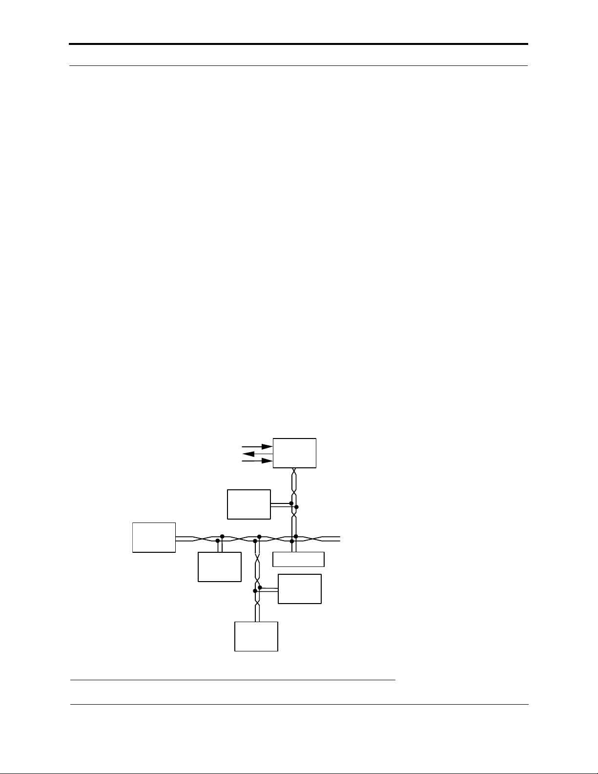
Power is supplied by a local +5VDC power supply located at each device as shown in Figure 1.2.
Smart
Transceiver
Device
Termination
Smart
Transceiver
Device
To additional
FT 3120 / FT 3150
Smart Transceiver
devices
Smart
Transceiver
Device
Sensor
Actuator
+5VDC power
Smart
Transceiver
Device
Smart
Transceiver
Device
Smart
Transceiver
Device
Figure 1.2 Free Topology Transceiver System
4 FT 3120/FT 3150 Smart Transceiver Data Book
Page 11
Related Documentation
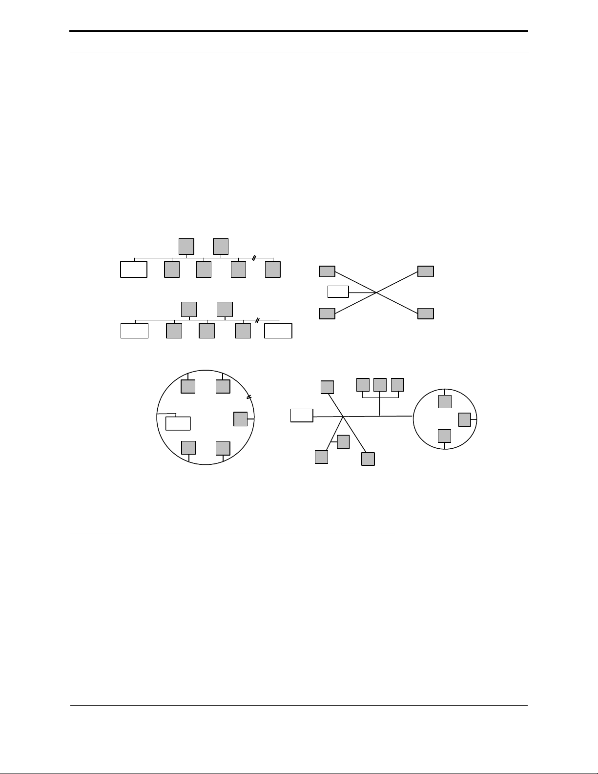
Unlike bus wiring designs, the free topology FT Smart Transceivers use a wiring scheme that supports star, loop, and/
or bus wiring (see Figure 1.3). This design has many advantages:
1. The installer is free to select the method of wiring that best suits the installation, reducing the need for advanced
planning and allowing last minute changes at the installation site.
2. If installers have been trained to use one style of wiring for all installations, free topology technology can be intro-
duced without requiring retraining.
3. Retrofit installations with existing wiring plants can be accommodated with minimal, if any, rewiring. This capa-
bility ensures that FT Smart Transceiver technology can be adapted to both old and new projects.
4. Free topology permits FT Smart Transceiver systems to be expanded in the future by simply tapping into the
existing wiring where it is most convenient to do so. This reduces the time and expense of system expansion, and
from the customer's perspective, keeps down the life cycle cost of the free topology network.
*
Singly Terminated Bus Topology
*
**
Doubly Terminated Bus Topology
Star Topology
*
*
Loop Topology Mixed Topology
(* = Termination. The actual termination circuit will vary by topology.)
Figure 1.3 Typical Wiring Topologies Supported by the FT Smart Transceivers System Content
Related Documentation
The following Echelon documents are suggested reading:
L
ONWORKS SMX Transceiver Datasheet (003-0336-01)
LonBuilder User's Guide (078-0001-01)
NodeBuilder User's Guide (078-0141-01)
Neuron C Programmer's Guide (078-0002-01)
LonBuilder Hardware Guide (078-0003-01)
FT 3120/FT 3150 Smart Transceiver Data Book 5
Page 12

Chapter 1 - Introduction
LONMARK™ Layers 1-6 Interoperability Guidelines (078-0014-01)
L
ONMARK
™
Application Layer Interoperability Guidelines (078-0120-01)
FT 3120 and FT 3150 Smart Transceiver Datasheet (003-0337-01)
L
ONWORKS FTT-10A Free Topology Transceiver data sheet (003-0312-01)
L
ONWORKS Custom Node Development engineering bulletin (005-0024-01)
LPI-10 Link Power Interface Module User’s Guide (078-0104-01)
LPT-10 Link Power Transceiver User's Guide (078-0105-01)
Junction Box and Wiring Guidelines for Twisted Pair L
ONWORKS Networks engineering bulletin (005-0023-01)
EIA-709.1 Control Network Protocol Specification (distibuted by Global Engineering Documents:
global.ihs.com).
6 FT 3120/FT 3150 Smart Transceiver Data Book
Page 13

2
Hardware Resources
FT 3120 / FT 3150 Smart Transceiver Data Book 7
Page 14
Chapter 2 - Hardware Resources
Overview
The FT 3150 Smart Transceiver supports external memory for more complex applications, while the FT 3120 Smart
Transceiver is a complete system on a chip. The major hardware blocks of both processors are the same, except where
noted in the table and figure below.
Table 2.1 Comparison of FT Smart Transceivers
Characteristic FT 3150 Smart Transceiver FT 3120 Smart Transceiver
RAM Bytes 2,048 2,048
ROM Bytes — 12,288
EEPROM Bytes 512 4,096
16-Bit Timer/Counters 2 2
External Memory Interface Ye s No
Package 64 pin TQFP 32 pin SOIC
44 pin TQFP
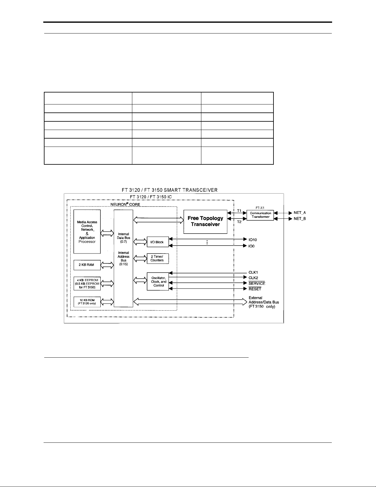
Figure 2.1 FT Smart Transceiver Block Diagram
Neuron Processor Architecture
The Neuron core is composed of three processors. These processors are assigned to the following functions by the
Neuron firmware.
Processor 1 is the MAC layer processor that handles layers 1 and 2 of the 7-layer LonTalk
includes driving the communications subsystem hardware and executing the media access control algorithm.
Processor 1 communicates with Processor 2 using network buffers located in shared RAM memory.
8 FT 3120 / FT 3150 Smart Transceiver Data Book
®
protocol stack. This
Page 15
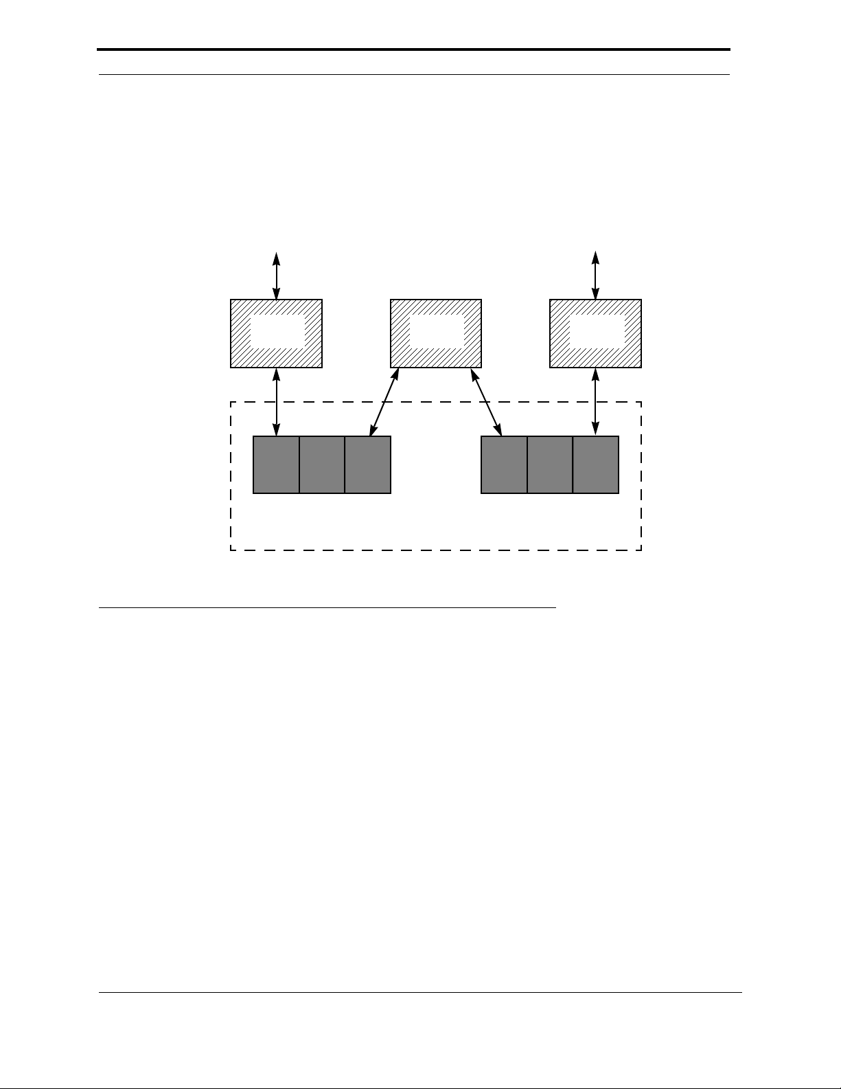
Neuron Processor Architecture
Processor 2 is the network processor that implements layers 3 through 6 of the LonTalk protocol stack. It handles
network variable processing, addressing, transaction processing, authentication, background diagnostics, software
timers, network management, and routing functions. Processor 2 uses network buffers in shared memory to
communicate with Processor 1, and application buffers to communicate with Processor 3. These buffers are also
located in shared RAM memory. Access to them is mediated with hardware semaphores to resolve contention when
updating shared data.
.
Communications
Port
Input/Output
MAC
Proces-
Network
Proces-
Application BuffersNetwork Buffers
Shared
Applica-
tion
Figure 2.2 Processor Organization Memory Allocation
Processor 3 is the application processor. It executes the code written by the user, together with the operating system
services called by user code. The primary programming language used by applications is Neuron C, a derivative of
the ANSI C language optimized and enhanced for L
ONWORKS distributed control applications. The major
enhancements are the following (see the Neuron C Programmer’s Guide for details):
• A network communication model, based on functional blocks and network variables, that simplifies and pro-
motes data sharing between like and disparate devices.
• A network configuration model, based on functional blocks and configuration properties, that facilitates
interoperable network configuration tools.
• A type model based on standard and user resource files that expands the market for interoperable devices by
simplifying the integration of devices from multiple manufacturers.
• An extensive set of I/O drivers that support the I/O capabilities of the Neuron core.
• Powerful event driven programming extensions that provide easy handling of network, I/O, and timer
events.
The support for all these capabilities is part of the Neuron firmware, and does not need to be written by the
programmer.
Each of the three identical processors has its own register set (Table 2.2), but all three processors share data, ALUs
(arithmetic logic units) and memory access circuitry (Figure 2.3). On the FT 3150 Smart Transceiver, the internal
FT 3120 / FT 3150 Smart Transceiver Data Book 9
Page 16
Chapter 2 - Hardware Resources
address, data, and R/W signals are reflected on the corresponding external lines when utilized by any of the internal
processors. Each CPU minor cycle consists of three system clock cycles, or phases; each system clock cycle is two
input clock cycles. The minor cycles of the three processors are offset from one another by one system clock cycle, so
that each processor can access memory and ALUs once during each instruction cycle. Figure 2.3 shows the active
elements for each processor during one of the three phases of a minor cycle. Therefore, the system pipelines the three
processors, reducing hardware requirements without affecting performance. This allows the execution of three
processes in parallel without time-consuming interrupts and context switching.
Table 2.2 Register Set
Mnemonic Bits Contents
FLAGS 8 CPU Number, Fast I/O Select, and Carry Bit
IP 16 Next Instruction Pointer
BP 16 Address of 256-Byte Base Page
DSP 8 Data Stack Pointer Within Base Page
RSP 8 Return Stack Pointer Within Base Page
TOS 8 Top of Data Stack, ALU Input
Processor 1
Registers
Memory
Processor 2
Registers
ALUs
Latch
Latch
Processor 3
Registers
Active elements – Processor 1
Active elements – Processor 2
Active elements – Processor 3
Figure 2.3 Processor/Memory Activity During One of the Three System Clock Cycles of a Minor Cycle
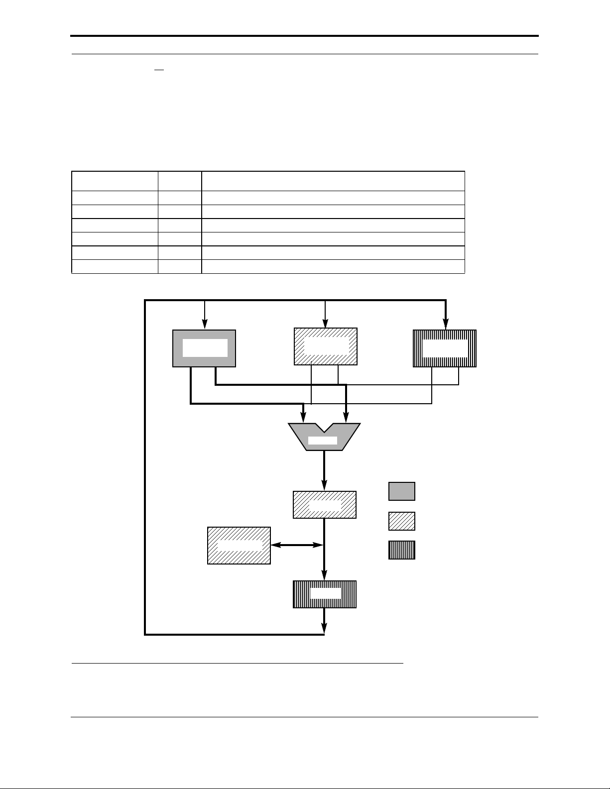
The architecture is stack-oriented; one 8-bit wide stack is used for data references, and the ALU operates on the TOS
(Top of Stack) register and the next entry in the data stack which is in RAM. A second stack stores the return
10 FT 3120 / FT 3150 Smart Transceiver Data Book
Page 17
Neuron Processor Architecture
addresses for CALL instructions, and may also be used for temporary data storage. This stack architecture leads to
very compact code. Tables 2.3, 2.42.4, and 2.5 outline the instruction set.
Figure 2.4 shows the layout of a base page, which may be up to 256 bytes long. Each of the three processors uses a
different base page, whose address is given by the contents of the BP register of that processor. The top of the data
stack is in the 8-bit TOS register, and the next element in the data stack is at the location within the base page at the
offset given by the contents of the DSP register. The data stack grows from low memory towards high memory. The
assembler shorthand symbol NEXT refers to the contents of the location (BP+DSP) in memory, which is not an actual
processor register.
Pushing a byte of data onto the data stack involves the following steps: incrementing the DSP register, storing the
current contents of TOS at the address (BP+DSP) in memory, and moving the byte of data to TOS.
Popping a byte of data from the data stack involves the following steps: moving TOS to the destination, moving the
contents of the address (BP+DSP) in memory to TOS, and decrementing the DSP register.
The return stack grows from high memory towards low memory. Executing a subroutine call involves the following
steps: storing the high byte of the instruction pointer register IP at the address (BP+RSP) in memory, decrementing
RSP, storing the low byte of IP at the address (BP+RSP) in memory, decrementing RSP, and moving the destination
address to the IP register.
Similarly, returning from a subroutine involves the following steps: incrementing RSP, moving the contents of
(BP+RSP) to the low byte of the IP register, incrementing RSP, and moving the contents of (BP+RSP) to the high
byte of IP.
Return Stack
BP+RSP
TOS
BP+DSP
BP+0x18
BP+0x17
Sixteen Byte Registers
BP+0x8
BP+0x7
BP*
*BP = Base Page.
NEXT
Data Stack
Four 16-bit
Pointer Registers
Figure 2.4 Base Page Memory Layout
A processor instruction cycle is three system clock cycles, or six input clock (CLK1) cycles. Most instructions take
between one and seven processor instruction cycles. At an input clock rate of 40MHz, instruction times vary between
0.15 µs and 1.05 µs. Execution time scales inversely with the input clock rate. The formula for instruction time is:
<Instruction Time> = <# Cycles> x 6 / <Input Clock>
Tables 2.3, 2.42.4, and 2.5 list the processor instructions, their timings (in cycles) and sizes (in bytes). This is
provided for purposes of calculating the execution time and size of code sequences. All programming of the FT Smart
Transceiver is done with Neuron C using a LonBuilder or NodeBuilder development tool. The Neuron C compiler
can optionally produce an assembly listing, and examining this listing can help the programmer to optimize his/her
Neuron C source code.
FT 3120 / FT 3150 Smart Transceiver Data Book 11
Page 18

Chapter 2 - Hardware Resources
Table 2.3 Program Control Instructions
Mnemonic Cycles Size (bytes) Description Comments
NOP 1 1 No operation
SBR 1 1 Short unconditional branch Offset 0 to 15
BR/BRC/
BRNC
SBRZ/SBRNZ 3 1 Short branch on TOS (not)
BRF 4 3 Unconditional branch far Absolute address
BRZ/BRNZ 4 2 Branch on TOS (not) zero Offset -128 to +127. Drops TOS
RET 4 1 Return from subroutine Drops two bytes from return
BRNEQ 4/6 3 Branch if TOS not equal
DBRNZ 5 2 Decrement [RSP] and branch
CALLR 5 2 Call subroutine relative Offset -128 to +127. Pushes two
CALL 6 2 Call subroutine Address in low 8KB. Pushes
CALLF 7 3 Call subroutine far Absolute address. Pushes two
2 2 Branch, branch on (not) carry Offset -128 to +127
Offset 0 to 15. Drops TOS
zero
stack
Offset -128 to +127. Drops TOS
(taken/not taken)
if not zero
if equal
Offset -128 to +127. If not
taken, drops one byte from
return stack
bytes to return stack
two bytes to return stack
bytes to return stack
Table 2.4 Memory/Stack Instructions
Mnemonic Cycles Size (bytes) Comments / Effective Address (EA)
PUSH TOS 3 1 Increment DSP, duplicate TOS into NEXT
DROP TOS 3 1 Move NEXT to TOS, decrement DSP
DROP_R TOS 6 1 Move NEXT to TOS, decrement DSP, return from
call
PUSH (NEXT, DSP, RSP,
FLAGS)
POP (DSP, RSP, FLAGS) 4 1 Pop processor register
DROP NEXT 2 1 Decrement DSP
DROP_R NEXT 5 1 Decrement DSP and return from call
PUSH/POP !D 4 1 Byte register [8 to 23]
PUSH !TOS 4 1 EA = BP + TOS, push byte to NEXT
POP !TOS 4 1 EA = BP + TOS, pop byte from NEXT
PUSH [RSP] 4 1 Push from return stack to data stack, RSP
DROP [RSP] 2 1 Increment RSP
PUSHS #literal 4 1 Push short literal value [0 to 7]
PUSH #literal 4 2 Push 8-bit literal value [0 to 255]
PUSHPOP 5 1 Pop from return stack, push to data stack
POPPUSH 5 1 Pop from data stack, push to return stack
LDBP address 5 3 Load base page pointer with 16-bit value
PUSH/POP [DSP][-D] 5 1 EA = BP + DSP - displacement [1 to 8]
PUSHD #literal 6 3 16-bit literal value (high byte first)
PUSHD [PTR] 6 1 Push from 16-bit pointer [0 to 3], high byte first
4 1 Push processor register
unchanged
12 FT 3120 / FT 3150 Smart Transceiver Data Book
Page 19

Memory Allocation
POPD [PTR] 6 1 Pop to 16-bit pointer [0 to 3], low byte first
PUSH/POP [PTR][TOS] 6 1 EA = (16-bit pointer) + TOS
PUSH/POP [PTR][D] 7 2 EA = (16-bit pointer) + displacement [0 to 255]
PUSH/POP absolute 7 3 Absolute memory address
IN/OUT 7 + 4n 1 Fast I/O instruction, transfer n bytes
Table 2.5 ALU Instructions
Mnemonic Cycles Size (bytes) Operation
INC/DEC/NOT 2 1 Increment/decrement/negate TOS
ROLC/RORC 2 1 Rotate left/right TOS through carry
SHL/SHR 2 1 Unsigned left/right shift TOS, clear carry
SHLA/SHRA 2 1 Signed left/right shift TOS into carry
ADD/AND/OR/XOR/ADC 4 1 Operate with NEXT on TOS, drop NEXT
ADD/AND/OR/XOR #literal 3 2 Operate with literal on TOS
(ADD/AND/OR/XOR)_R 7 1 Operate with NEXT on TOS, drop NEXT and
return
ALLOC #literal 3 1 Add [1 to 8] to data stack pointer
DEALLOC_R #literal 6 1 Subtract [1 to 8] from data stack pointer and return
SUB NEXT,TOS 4 1 TOS = NEXT - TOS, drop NEXT
SBC NEXT, TOS 4 1 TOS = NEXT - TOS - carry, drop NEXT
SUB TOS,NEXT 4 1 TOS = TOS - NEXT, drop NEXT
XCH 4 1 Exchange TOS and NEXT
INC [PTR] 6 1 Increment 16-bit pointer [0 to 3]
Memory Allocation
FT 3120 Smart Transceiver
See Figure 2.6 for a memory map of the FT 3120 Smart Transceiver.
• 4,096 bytes of in-circuit programmable EEPROM that store:
— Network configuration and addressing information.
— Unique 48-bit Neuron ID (written at the factory).
— User-written application code and read-mostly data.
• 2,048 bytes of static RAM that store the following:
— Stack segment, application, and system data.
— Network buffers and application buffers.
• 12,288 bytes of ROM that store the following:
— The Neuron firmware, including the system firmware executed by the MAC and network processors, and
the executive supporting the application program.
FT 3150 Smart Transceiver
See Figure 2.5 for a memory map of the FT 3150 Smart Transceiver.
• 512 bytes of in-circuit programmable EEPROM that store the following:
— Network configuration and addressing information.
FT 3120 / FT 3150 Smart Transceiver Data Book 13
Page 20
Chapter 2 - Hardware Resources
r
— Unique 48-bit Neuron ID (written at the factory).
— User-written application code and read-mostly data. See Table 2.6 for available EEPROM space.
• 2,048 bytes of static RAM that store the following:
— Stack segment, application, and system data.
— Network and application buffers.
• The processor can access 59,392 bytes of the available 65,536 bytes of memory address space via the exter-
nal memory interface. The remaining 6,144 bytes of the memory address space are mapped internally.
• 16,384 bytes of the external memory (59,392 bytes total) are required to store the following:
— The Neuron firmware, including the system firmware executed by the MAC and Network processors, and
the executive supporting the application program.
• The rest of the external memory (43,008 bytes) is available for:
— User-written application code.
— Additional application read/write and non-volatile data.
— Additional network buffers and application buffers.
FFFF
FC00
FBFF
F200
F1FF
F000
EFFF
E800
E7FF
4000
3FFF
0000
1K Reserved Space For
Memory Mapped I/O
2.5K Reserved Space
0.5K EEPROM
2K RAM
42K of Memory
Space Available
to the User
16K Neuron
Firmware and
Reserved Space
Figure 2.5 FT 3150 Smart Transceiver
Memory Map
Internal
External
FFFF
FC00
FBFF
F000
EFFF
E800
4FFF
4C00
2FFF
0000
1K Reserved Space For
Memory Mapped I/O
3K EEPROM
2K RAM
Unavailable
1K EEPROM
Unavailable
12K Neuron Firmware
(ROM)
Figure 2.6 FT 3120 Smart Transceive
Memory Map
Internal
EEPROM
Both versions of the FT Smart Transceiver have internal EEPROM containing:
• Network configuration and addressing information.
14 FT 3120 / FT 3150 Smart Transceiver Data Book
Page 21

Memory Allocation
• Unique 48-bit Neuron ID.
• Optional user-written application code and data tables.
All but 8 bytes of the EEPROM can be written under program control using an on-chip charge pump to generate the
required programming voltage. The charge pump operation is transparent to the user. The remaining 8 bytes are
written during manufacture, and contain a unique 48-bit identifier for each part called the Neuron ID, plus 16 bits for
the device code of the chip manufacturer. Each byte in the EEPROM region may be written up to 10,000 times. For
both the FT Smart Transceivers, the EEPROM stores the installation-specific information such as network addresses
and communications parameters. For the FT 3120 Smart Transceiver, the EEPROM also stores the application
program generated by the LonBuilder or NodeBuilder development tools. The application code for the FT 3150
Smart Transceiver may be stored either on-chip in the EEPROM memory or off-chip in external memory depending
on the size of the application code. See Table 2.6 for available EEPROM space.
For all write operations to the internal EEPROM, the Neuron firmware automatically compares the value in the
EEPROM location with the value to be written. If the two are the same, the write operation is not performed. This
prevents unnecessary write cycles to the EEPROM, and reduces the average EEPROM write cycle latency.
When the FT Smart Transceiver is not within the specified power supply voltage range, a pending or on-going
EEPROM write is not guaranteed. The FT Smart Transceiver contains a built-in low-voltage interruption (LVI)
circuit that holds the chip in reset when V
Transceiver Datasheet for LVI trip points. This prevents EEPROM data corruption, although in some cases,
additional external protection may be appropriate. See section , RESET Pin, for more information on LVI circuitry.
In the event of a fault, the on-chip EEPROM of the FT 3150 Smart Transceiver can be reset to its factory default state
by executing the EEBLANK program. To do so, program the EEBLANK.NRI file into an external memory device,
temporarily replace the external ROM or flash for the application with the chip that has EEBLANK.NRI loaded, and
power up the device.
is below a certain voltage. See the FT 3120 and FT 3150 Smart
CC
After some time, the service LED of the device should come on solid, indicating that the EEPROM has been blanked.
Then replace the original application ROM or flash. The EEBLANK.NRI file is distributed with the LonBuilder 3.01
(Service Pack 5), NodeBuilder 1.5 (Service Pack 8 or greater), and NodeBuilder 3 (Service Pack 1 or greater)
development tools. The file may also be downloaded from the developer’s toolbox located on the Echelon website
(www.echelon.com). Versions of EEBLANK.NRI distributed before these Service Packs should not be used with
the FT 3150 Smart Transceiver.
The set_eeprom_lock() function can also be used for additional protection against accidental EEPROM data
corruption. This function allows the application program to set the state of the lock on the checksummed portion of
the EEPROM. Refer to the Neuron C Reference Guide for more information.
The internal EEPROM of a FT Smart Transceiver will contain a fixed amount of overhead and a network image
(configuration), in addition to user code and user data. The following table shows the maximum amount of EEPROM
space available for user code and user data assuming a minimally-sized network image. Also shown is the minimum
segment size for user data. Constant data is assumed to be part of the code space.
Table 2.6 Memory Usage
Device Firmware Version
FT 3120 Smart Transceiver 13 3969 8
FT 3150 Smart Transceiver 13 384 2
EEPROM Space
(Bytes)
Segment Size
(Bytes)
EEPROM must be allocated in increments of the device's segment size, the smallest unit of EEPROM that can be
allocated for variable space. For example, if there are three 3-byte variables used, there must be 9 bytes of variable
space. For an FT 3120 Smart Transceiver, this would result in the allocation of 16 bytes for variable space, as 16
bytes is the lowest increment of the device segment size (8 bytes) that can store the three 3-byte variables. For an FT
3150 Smart Transceiver, this would result in the allocation of 10 bytes for variable space, as 10 bytes is the lowest
increment of the device segment size (2 bytes) that can store the three 3-byte variables.
FT 3120 / FT 3150 Smart Transceiver Data Book 15
Page 22

Chapter 2 - Hardware Resources
Static RAM
Both FT Smart Transceivers contain 2048 bytes of static RAM. The RAM is used to store the following:
• Stack segment, application, and system data
• Network buffers and application buffers
The RAM state is retained as long as power is applied to the device. After reset, releasing the FT Smart Transceiver
initialization sequence will clear the RAM (see the section Reset Processes and Timing, later in this chapter).
Preprogrammed ROM
The FT 3120 Smart Transceiver contains 12,288 bytes of pre-programmed ROM. This memory contains the Neuron
firmware, including the LonTalk protocol stack, real time task scheduler, and system function libraries. The Neuron
firmware for the FT 3150 Smart Transceiver is stored in external memory. The object code is supplied with the
LonBuilder and NodeBuilder tools.
External Memory of the FT 3150 Smart Transceiver
External memory is support only for the FT 3150 Smart Transceiver. The memory interface supports up to 42Kbytes
of external memory space for additional user program and data. The total address space is 64Kbytes. However, the
upper 6K of address space is reserved for internal RAM, EEPROM, and memory-mapped I/O (see Figure 2.5 and
Figure 2.6), leaving 58K of external address space. Of this space, 16K is used by the Neuron firmware and is reserved
for other specific functions. The external memory space can be populated with RAM, ROM, PROM, EPROM,
EEPROM, or flash memory in increments of 256 bytes. The memory map for the FT 3150 Smart Transceiver is
shown in Figure 2.5. The bus has 8 bidirectional data lines and 16 address lines driven by the processor. Two interface
lines (R/W
Datasheet for the required access times for the external memory used. If the input clock is scaled down, slower
memory can be used. The input clock rates supported by the FT 3150 Smart Transceiver are 20MHz, 10MHz, and
5MHz. The Enable Clock (E
internal and external, may be accessed by any of the three processors at the appropriate phase of the instruction cycle.
Since the instruction cycles of the three processors are offset by one-third of a cycle with respect to each other, the
memory bus is used by only one processor at a time.
and E) are used for external memory access. Refer to the FT 3120 and FT 3150 Smart Transceiver
) runs at the system clock rate, which is one-half the input clock rate. All memory, both
The Neuron 3150 Chip External Memory Interface engineering bulletin provides guidelines for interfacing the FT
3150 Smart Transceiver to different types of memory. A minimum hardware configuration would use one external
ROM (PROM or EPROM), containing both the Neuron firmware and user application code. This configuration
would not allow the system engineer to change the application code after installation. The network image (network
address and connection information) however, could be altered because this information resides in internal
EEPROM. If application downloads over the network are a requirement for maintenance or upgrade and the
application code will not fit into the internal EEPROM, then external EEPROM or flash will be necessary. Refer to
the Neuron C Programmer’s Guide for guidelines to reduce code size.
The pins used for external memory interfacing are listed in Table 2.7. The E
write) signals to external memory. The A15 (address line 15) or a programmable array logic (PAL) decoded signal
gated with R/W
16 FT 3120 / FT 3150 Smart Transceiver Data Book
can be used to generate read signals to external memory.
clock signal is used to generate read (or
Page 23

Input/Output
Table 2.7 External Memory Interface Pins
Pin Designation Direction Function
A0 – A15 Output Address Pins
D0 – D7 Input/Output Data Pins
E Output Enable Clock
R/W Output Read/Write Select Low
The preferred method of interfacing the FT Smart Transceiver to another MPU is through the 11 I/O pins using a
serial or parallel connection, or through a dual-ported RAM device such as the Cypress CY7C144, CY7C138, or
CY7C1342. There are pre-defined serial and parallel I/O models for this purpose which are easily implemented using
the Neuron C programming language, or the short stack or MIP firmware can be used to simplify the interface. For
more details of dual-ported RAM interfacing, see Appendix B of the L
User’s Guide (Echelon 078-0017-01).
ONWORKS Microprocessor Interface Program
Input/Output
Eleven Bidirectional I/O Pins
These pins are usable in several different configurations to provide flexible interfacing to external hardware and
access to the internal timer/counters. The logic level of the output pins may be read back by the application processor.
See Section 6 for detailed electrical characteristics.
Pins IO4 – IO7 have programmable pull-up current sources. They are enabled or disabled with a compiler directive
(see the Neuron C Reference Guide). Pins IO0 – IO3 have high current sink capability (20 mA @ 0.8 V). The others
have the standard sink capability (1.4 mA @ 0.4 V). All pins (IO0 – IO10) have TTL level inputs with hysteresis.
Pins IO0 – IO7 also have low level detect latches.
Two 16-Bit Timer/Counters
The timer/counters are implemented as a load register writable by the processor, a 16-bit counter, and a latch readable
by the processor. The 16-bit registers are accessed 1 byte at a time. Both the FT 3120 and FT 3150 Smart
Transceivers have one timer/counter whose input is selectable among pins IO4 – IO7, and whose output is pin IO0,
and a second timer/counter with input from pin IO4 and output to pin IO1 (Figure 2.7). No I/O pins are dedicated to
timer/counter functions. If, for example, Timer/Counter 1 is used for input signals only, then IO0 is available for other
input or output functions. Timer/counter clock and enable inputs may be from external pins, or from scaled clocks
derived from the system clock; the clock rates of the two timer/counters are independent of each other. External clock
actions occur optionally on the rising edge, the falling edge, or both rising and falling edges of the input.
FT 3120 / FT 3150 Smart Transceiver Data Book 17
Page 24
Chapter 2 - Hardware Resources
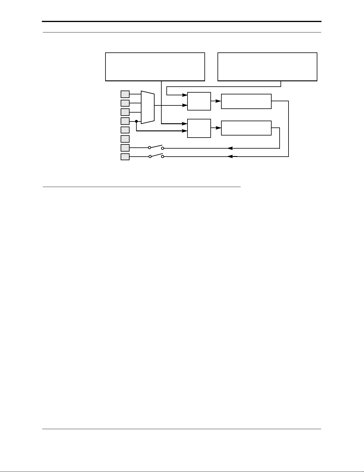
IO7
IO6
IO5
IO4
IO3
IO2
IO1
IO0
System Clock Divide
Chain
Control
Logic
MUX
Control
Logic
System Clock Divide
Chain
Timer/Counter 1
Timer/Counter 2
Figure 2.7 Timer/Counter Circuits
Clock Input
The FT Smart Transceivers operate with an input clock of 5, 10, or 20MHz. The FT 3120 Smart Transceiver also
supports 40MHz operation. Developers who are using the LonBuilder 3.0.1 or NodeBuilder 1.5 tools and are
upgrading to a clock speed higher than 10MHz should refer to the readme.txt file included in the latest Service Pack
for the LonBuilder 3.01, or for NodeBuilder 1.5 tools for an in-depth discussion about the software considerations on
each platform. The NodeBuilder 3.2 (or later) development tool contains built-in support for these higher clock
speeds.
Clock Generation
The FT Smart Transceiver divides the input clock by a factor of two to provide a symmetrical on-chip system clock.
The input clock may be generated either by an external free-running oscillator or by the on-chip oscillator in the
Smart Transceiver using an external parallel-mode resonant crystal.
The accuracy of the input clock frequency of the FT Smart Transceiver must be ±200ppm or better; this requirement
can be met with a suitable crystal, but cannot be met with a ceramic resonator.
The FT Smart Transceiver includes an oscillator that may be used to generate an input clock using an external crystal.
For 5 MHz, 10MHz, and 20MHz, either an external clock source or the on-chip crystal oscillator may be used. For
40MHz operation of an FT 3120 Smart Transceiver, an external oscillator must be used.
When an externally generated clock is used to drive the CLK1 CMOS input pin of the FT Smart Transceiver, CLK2
must be left unconnected or used to drive no more than one external CMOS load. The accuracy of the clock
frequency must be ± 0.02% (200 ppm) or better, to ensure that devices may correctly synchronize their bit clocks.
Figure 2.8 shows the crystal oscillator circuit. Use the load capacitance and resistor values recommended by the
manufacturer of the crystal for this circuit. A 60/40 duty cycle or better is required when using an external oscillator
as shown in Figure 2.9. An external oscillator must provide CMOS voltage levels to the CLK1 pin.
18 FT 3120 / FT 3150 Smart Transceiver Data Book
Page 25
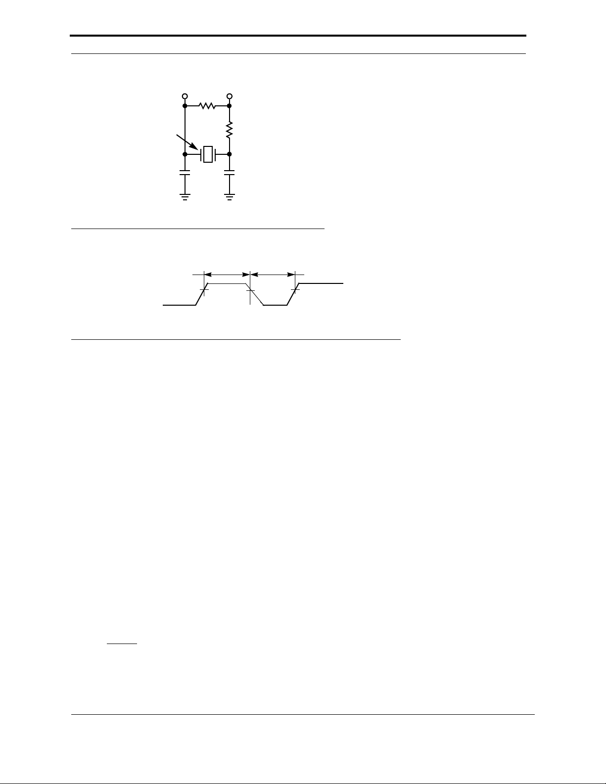
CLK 2CLK1
R
f
EXTERNAL
CRYSTAL
CC
R
Figure 2.8 Smart Transceiver Clock Generator Circuit
Additional Functions
PW
HIGH
VDD /2VDD /2
PW
LOW
V
/2
DD
Figure 2.9 Test Point Levels for CLK1 Duty Cycle Measurements
The FT 3120 Smart Transceiver was designed to run at frequencies up to 40MHz using an external clock oscillator.
External oscillators generally take several milliseconds to stabilize after power-up. The FT 3120 Smart Transceiver
operating at 40MHz must be held in reset until the externally-generated CLK input is stable, so an external poweron-reset-pulse stretching LVI chip/circuit is required. Check the specification of the oscillator vendor for more
information about startup stabilization times.
Additional Functions
Reset Function
The reset function is a critical operation in any embedded microcontroller. In the case of theFT 3120 and FT 3150
Smart Transceivers, the reset function plays a key role in the following conditions:
• Initial V
• V
DD
• Program recovery (if an application gets lost due to corruption of address or data, an external reset can be
used for recovery or the watchdog timer could timeout, causing a watchdog reset).
• V
DD
• Helps protect the EEPROM from major corruption.
power up (ensures proper initialization of the FT Smart Transceiver).
DD
power fluctuations (manages proper recovery of FT Smart Transceiver after VDD stabilizes).
power down (ensures proper shut down).
The FT Smart Transceivers have four mechanisms to initiate a reset:
• RESET pin is pulled low and then returned high.
• Watchdog timeout occurs during application execution (the timeout period is 210ms at 40MHz; this figure
scales inversely with clock frequency).
FT 3120 / FT 3150 Smart Transceiver Data Book 19
Page 26

Chapter 2 - Hardware Resources
• Software command either the from the application program or from the network.
• LVI circuit detects a drop in the power supply below a set level.
During any of the reset functions, when the RESET
states described in the list below. Figure 2.11 also illustrates the condition of the pins during reset and the FT Smart
Transceivers initialization sequence after reset is returned high again.
pin is in the low state, the FT Smart Transceiver pins go to the
• Oscillator continues to run
• All processor functions stop
• SERVICE pin goes to high impedance
• I/O pins go to high impedance
• All output address pins go to 0xFFFF (FT 3150 Smart Transceiver only)
• All data pins become outputs with high or low states (FT 3150 Smart Transceiver only)
• E clock goes high (FT 3150 Smart Transceiver only)
• R/W goes low (FT 3150 Smart Transceiver only)
When the RESET
starting at address 0x0001. The time it takes the FT Smart Transceiver to complete its initialization differs between
FT Smart Transceivers, the different firmware versions that are being run, and the memory space used by the
application (code and data). This will be discussed later in this section.
pin is released back to a high state, the FT Smart Transceiver begins its initialization procedure
RESET Pin
The RESET pin is both an input and an output. As an input, the RESET pin is internally pulled high by a current
source acting as a pull-up resistor. The RESET
pin becomes an output when any of the following events occur:
• Watchdog Timer event.
• Software reset initialization.
• Internal LVI detects a low voltage.
• RESET pin drops below the internal trip point.
Power Up Sequence
During power up sequences, the RESET
malfunctioning. Likewise, when powering down, the FT Smart Transceiver RESET
before the power supply goes below the minimum operating voltage of the FT Smart Transceiver.
WARNING: If proper reset recovery circuitry is not used, the FT Smart Transceiver can go applicationless or
unconfigured. The applicationless or unconfigured state occurs when the checksum error verification routine detects
a corruption in memory which could have falsely been detected due to improper reset sequence or noise on the power
supply. Several options exist in the LonBuilder and NodeBuilder tools to allow a reboot on checksum failure.
Figure 2.11 shows typical external RESET
including stray and external device input capacitance, must not exceed 1000 pF. This ensures that the FT Smart
Transceiver can successfully output a reset down to below 0.8V. The 100 pF minimum capacitance is required for
noise immunity.
pin should be held low until the power supply is stable, to prevent start-up
pin should go to a low state
components. The total capacitance directly connected to the RESET pin,
20 FT 3120 / FT 3150 Smart Transceiver Data Book
Page 27
Software Controlled Reset
Additional Functions
When the CPU watchdog timer expires, or a software command to reset occurs, the RESET
CLK1 clock cycles. The RESET
pin and external capacitor (100 ≤ x ≤ 1000 pF) are allowed to begin charging and
provide the required duration of reset.
Smart Transceiver
5V V
DD
To O t her
Devices
IN
LV I
GND
If using flash, an external pulse-stretching LVI must be used
(Dallas DS1233-10).
RESET
C
E
(100 pF Min
1000 pF Max)
Switch
RESET
Figure 2.10 Example of a Reset Circuit
pin is pulled low for 256
Watchdog Timer
The FT Smart Transceivers are protected against malfunctioning software or memory faults by three watchdog
timers, one for each processor that makes up the Neuron core. If application or system software fails to reset these
timers periodically, the entire FT Smart Transceiver is automatically reset. The watchdog period is approximately 210
ms at a 40MHz input clock rate and scales inversely with the input clock rate.
LVI Considerations
The FT 3120 and FT 3150 Smart Transceivers include an internal LVI to ensure that they only operate above the
minimum voltage threshold. See the FT 3120 and FT 3150 Smart Transceiver Datasheet for LVI trip points. If the
circuit operates below this voltage, improper operation could occur. For example, if the FT Smart Transceiver is
writing to an internal or external EEPROM or to flash memory when a reset event is initiated, then that data could be
corrupted.
When using external flash memory for the FT 3150 Smart Transceiver device, an external pulse-stretching LVI of
greater than 50 ms should be used (Echelon recommends using Dallas Semiconductor Part No. DS1233-5). When
using an external oscillator to drive the CLK1 pin of either of the FT Smart Transceivers, a power-on-pulse-stretching
LVI may be needed to ensure that the external oscillator has stabilized before the FT Smart Transceiver is released
from reset.
Since the RESET
collector output. If an external LVI actively drives the RESET
able to reliably assert the RESET
RESET
pin can cause anomalous behavior, from applicationless errors to physical damage to the FT Smart
pin of the FT Smart Transceiver is bidirectional, an external LVI must have an open-drain or open-
pin high, then the FT Smart Transceiver will not be
pin (low) during internal resets. This contention on the FT Smart Transceiver
Transceiver reset circuitry.
FT 3120 / FT 3150 Smart Transceiver Data Book 21
Page 28

Chapter 2 - Hardware Resources
Reset Processes and Timing
During the reset period, the I/O pins are in a high-impedance state. The FT 3150 Smart Transceiver address lines A15
– A0 are forced to 0xFFFF, R/W
or low, so they will not float and draw excess current. The SERVICE
overrides the effect of E
during the E
preparing the FT Smart Transceiver to execute the application code are discussed below. These steps are summarized
in Figure 2.11.
clock low portion of the bus cycle, while reset forces the data bus to be driven. The steps followed in
clock on data lines in that, in normal operations the data bus is only driven in a write cycle
is forced to 0, and E is forced to 1. The data lines are undetermined but driven high
pin is high impedance during reset. Reset
After the RESET
executing application programs. These tasks are:
pin is released, the FT Smart Transceiver performs hardware and firmware initialization before
• Oscillator start-up
• Oscillator stabilization
• Stack initialization and built-in self-test (BIST)
• SERVICE pin initialization
• State initialization
22 FT 3120 / FT 3150 Smart Transceiver Data Book
Page 29
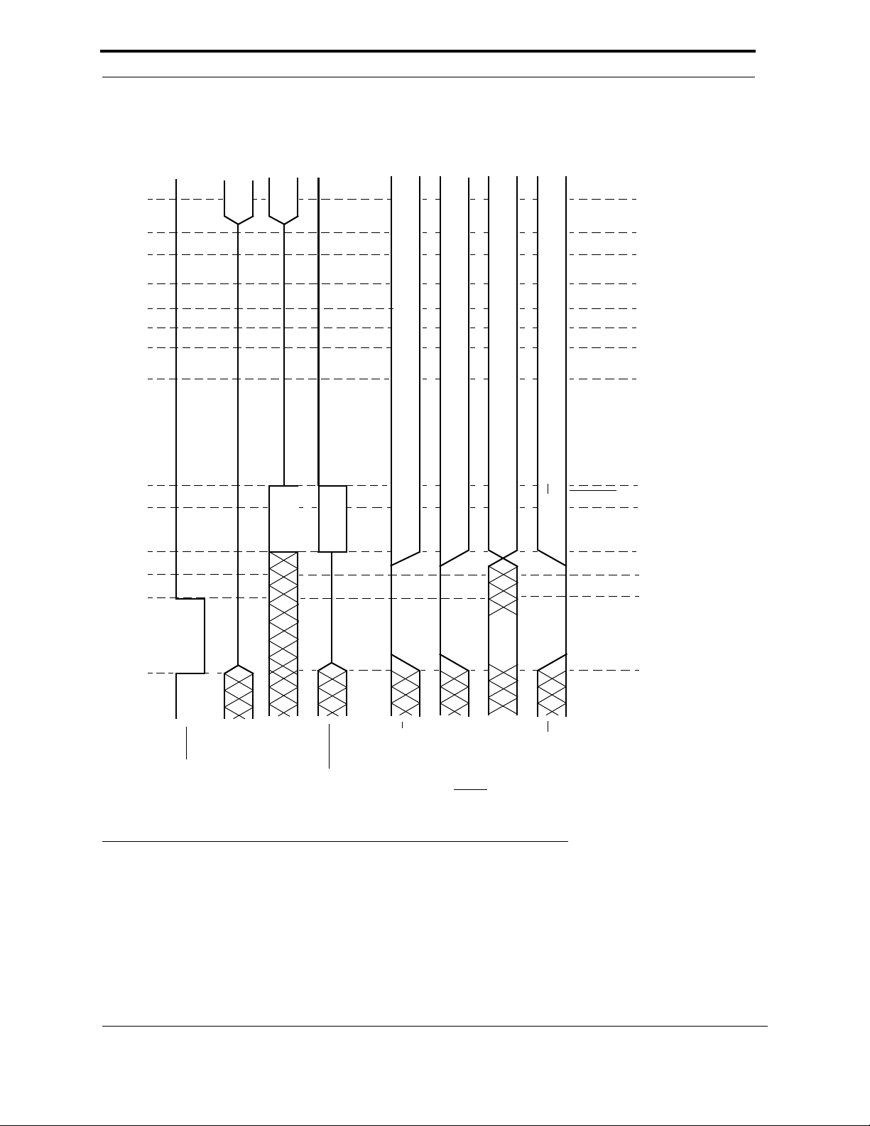
Additional Functions
Specified by Application
Specified by Application
Enabled
Pull-Ups
Oscillates
Oscillates at Divide by 2 of CLK1
Stable Address Reflecting Firmware Execution
Stable Data Reflecting Firmware Execution
Scheduler Init
One-Second Timer Init
Checksum Init
Comm Port Init
System RAM Setup
Random Number Seed Calc
Off-Chip RAM
State Init
SERVICE
Stack Init and BIST
Stable R/W Reflecting Firmware Execution
Oscillator Stabilization*
Oscillator Start-Up*
Low
Pin Init
Output
High or Low
E
RESET
IO [10:8, 3:0]
*NOTE: On power up, the oscillator will start running before RESET is released.
IO [7:4]
FT 3150 ONLY
SERVICE
ADDR [15:0]
DATA [7:0]
Reset
R/W
WARNING: NOT TO SCALE
Figure 2.11 RESET Timeline for FT 3120 and FT 3150 Smart Transceivers
• Off-chip RAM initialization
• Random number seed calculation
• System RAM setup
• Communication port initialization
• Checksum initialization
FT 3120 / FT 3150 Smart Transceiver Data Book 23
Page 30

Chapter 2 - Hardware Resources
• One-second timer initialization
• Scheduler initialization
During internal oscillator start up (after power up), the FT Smart Transceiver waits for the oscillator signal amplitude
to grow before using the oscillator waveform as the system clock. This period depends on the type of oscillator used
and its frequency, and begins as soon as power is applied to the oscillator and is independent of the RESET
oscillator start-up period may end before or after RESET
is released, depending on the duration of reset and the time
required by the oscillator to start up.
After the oscillator has started up, the FT Smart Transceiver counts additional transitions on CLK1 to allow the
frequency of the oscillator to stabilize. From the time RESET
period, the I/O pins are in a high-impedance state. The E
is asserted until the end of the oscillator stabilization
signal goes inactive (high) immediately after reset goes low,
and the address bus becomes high (0xFFFF) to deselect external devices.
The stack initialization and BIST task tests the on-chip RAM, the timer/counter logic, and the counter logic. For the
test to pass, all three processors and the ROM must be functioning. A flag is set to indicate whether the FT Smart
Transceiver passed or failed the BIST. The RAM is cleared to all 0s by the end of this step. At the beginning of this
task, the pull-ups on IO[7:4] are enabled, so that a weak high state can be observed on these pins. The SERVICE
oscillates between a solid low and a weak high. The memory interface signals reflect execution of these tasks.
If the RAM self-test fails, the device goes offline, the service LED comes on solid, and an error is logged in the status
structure of the device.
Self-test results are available in the first byte of RAM (0xE800) as follows:
pin. The
pin
Va lu e Description
0 No Failure
1 RAM failure
2 Timer/counter failure
3 Counter failure
4 Configured input clock rate exceeds the chip maximum
The SERVICE
pin initialization task turns off the SERVICE pin (high state).
The state initialization task determines if a FT Smart Transceiver boot is required (FT 3150 Smart Transceiver only),
and performs the boot if it is required. The FT Smart Transceiver decides to perform a boot if it is blank, or if the boot
ID does not match the boot ID in ROM.
The off-chip RAM initialization task checks the memory map to determine if any off-chip RAM is present and then
either tests and clears all of the off-chip RAM or, optionally, clears the application RAM area only. This choice is
controlled by the application program via a Neuron C compiler directive. This task applies only to the FT 3150 Smart
Transceiver.
The random number seed calculation task creates a seed for the random number generator.
The system RAM setup task sets up internal system pointers as well as the linked lists of system buffers.
The checksum initialization task generates or checks the checksums of the nonvolatile writable memories. If the boot
process was executed for the configured or unconfigured states, in the state initialization task, then the checksums are
generated; otherwise, they are checked. This process includes on-chip EEPROM, off-chip EEPROM, flash, and offchip nonvolatile RAM. There are two checksums, one for the configuration image and one for the application image.
In each case, the checksum is a negated two’s complement sum of the values in the image.
The one-second timer initialization task initializes the one-second timer. At this point, the network processor is
available to accept incoming packets.
The scheduler initialization task allows the application processor to perform application-related initialization as
follows:
24 FT 3120 / FT 3150 Smart Transceiver Data Book
Page 31

Additional Functions
• State w ait — wait for the device to leave the applicationless state.
• Pointer initialization — perform a global pointer initialization.
• Initialization step — execute initialization task, which is created by the compiler/linker to handle initializa-
tion of static variables and the timer/counters.
• I/O pin initialization step — initialize I/O pins based on application definition. Prior to this point, I/O pins
are high impedance.
• State w ait I I — wait for the device to leave the unconfigured or hard-offline state. If waiting was required, a
flag is set to indicate that the device should come up offline.
• Parallel I/O synchronization — devices using parallel I/O attempt to execute the master/slave synchroni-
zation protocol at this point.
• Reset task — execute the application reset task (when (reset{})).
If the offline flag was set, go offline and execute the offline task. If the BIST flag indicated a failure, then the
SERVICE
loop.
The amount of time required to perform these steps depends on many factors, including: FT Smart Transceiver
model; input clock rate; whether or not the device performs a boot process; whether the device is applicationless,
configured, or unconfigured; amount of off-chip RAM; whether the off-chip RAM is tested or simply cleared; the
number of buffers allocated; and application initialization. Table 2.8 and Table 2.9 summarize the number of input
clock cycles (CLK1) required for each of these steps for the FT 3120 and the FT 3150 Smart Transceivers. The times
are approximate and are given as functions of the most significant application variables.
pin is turned on and the offline task is executed. Otherwise, the scheduler starts its normal task scheduling
Table 2.8 FT 3120 Smart Transceiver Reset Sequence Time
Step Number of CLK1 Cycles Notes
Stack Initialization and BIST 386,000
SERVICE Pin Initialization 1000
State Initialization 250 (for no boot)
2,275,000 (for boot)
Off-Chip RAM Initialization 0
Random Number Seed Calculation 0 1
System RAM Set-up 21,000 + 600*B 2
Communication Port Initialization 0 1
Checksum Initialization 3400 + 175*M 3
One-Second Timer Initialization 6100
Scheduler Initialization ≥ 7400 4
Notes:
Note 1) These tasks run in parallel with other tasks.
Note 2) B is the number of application and/or network buffers allocated.
Note 3) M is the number of bytes to be checksummed.
Note 4) Assumes a trivial initialization task, no reset task and the configured state.
For example, the timing of each of these steps is shown for a FT 3120 Smart Transceiver application with the
following parameters: 10MHz input clock, crystal oscillator, no boot required, at least 10 application and/or network
buffers, and 500 bytes of EEPROM checksummed.
Stack Initialization and BIST 38.6 ms
SERVICE
Pin Initialization 0.1 ms
State Initialization 0.025 ms
Off-Chip RAM Initialization 0 ms
Random Number Seed Calculation 0 ms
FT 3120 / FT 3150 Smart Transceiver Data Book 25
Page 32

Chapter 2 - Hardware Resources
System RAM Setup 2.7 ms
Communication Port Initialization 0 ms
Checksum Initialization 10.8 ms
One-Second Timer Initialization 0.61 ms
Scheduler Initialization 0.74 ms
Total 53.7 ms
Table 2.9 FT 3150 Smart Transceiver Reset Sequence Time
Step Number of CLK1 Cycles Notes
Stack Initialization and BIST 425,000
SERVICE Pin Initialization 1000
State Initialization 1300 (for no boot)
70,000 + 25 ms*E (for boot)
Off-Chip RAM Initialization 24,000 + 214*R (for test and clear)
24,000 + 152*R
Random Number Seed Calculation 50,000 max
System RAM Setup 27,000 + 1500*B 4
Communication Port Initialization 0 5
Checksum Initialization 7200 + 175*M (for no boot)
82,000 + 100 ms + 175*M (for boot)
One-Second Timer Initialization 6100
Scheduler Initialization ≥ 7400 8
Notes:
Note 1) E is the number of non-zero bytes being written (ranges from 10 to 504).
Note 2) R is the number of off-chip RAM bytes.
Note 3) R
Note 4) B is the number of application and/or network buffers allocated.
Note 5) These tasks run in parallel with other tasks.
Note 6) M is the number of bytes to be checksummed.
Note 7) Only if booting to the configured or unconfigured state; if booting to the applicationless state, use the “no boot” equation.
Note 8) Assumes a trivial initialization task, no reset task, and the configured state.
is the number of non-system off-chip RAM bytes.
a
(for clear only)
a
1
2
3
6, 7
For example, the timing of each of these steps is shown for a FT 3150 Smart Transceiver application with the
following parameters: 10MHz input clock, crystal oscillator, no boot required, 16K external RAM, test and clear
external RAM, at least 10 application and/or network buffers, and 500 bytes of EEPROM checksummed.
Stack Initialization and BIST 42.5 ms
SERVICE
Pin Initialization 0.1 ms
State Initialization 0.13 ms
Off-Chip RAM Initialization 353 ms
Random Number Seed Calculation 5 ms
System RAM Setup 4.2 ms
Communication Port Initialization 0 ms
Checksum Initialization 12.5 ms
One-Second Timer Initialization 0.61 ms
Scheduler Initialization 0.74 ms
Total 418 ms
Use the following compiler directive to disable testing of off-chip RAM:
# pragma ram_test_off
26 FT 3120 / FT 3150 Smart Transceiver Data Book
Page 33
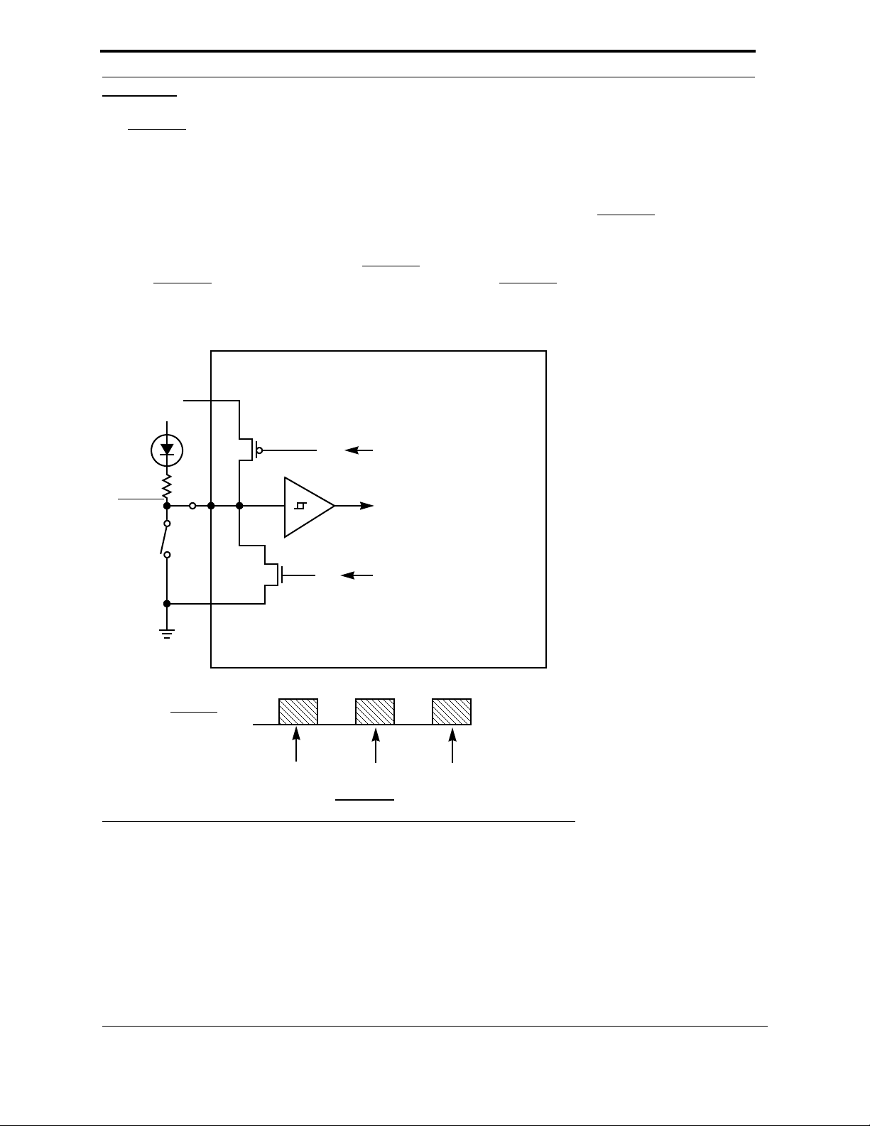
Additional Functions
SERVICE Pin
The SERVICE pin alternates between input and open-drain output at a 76 Hz rate with a 50% duty cycle. When it is
an output, it can sink 20 mA for use in driving a LED. When it is used exclusively as an input, it has an optional onchip pull-up to bring the input to an inactive-high state for use when the LED and pull-up resistor are not connected.
Under control of the Neuron firmware, this pin is used during configuration, installation, and maintenance of the
device containing the FT Smart Transceiver. The firmware flashes the LED at a 1/2-Hz rate when the FT Smart
Transceiver has not been configured with network address information. Grounding the SERVICE
Smart Transceiver to transmit a network management message containing its unique 48-bit Neuron ID and the
program ID of the application on the network. This information may then be used by a network tool to install and
configure the device. A typical circuit for the SERVICE
reset the SERVICE
pin state is indeterminate. The default state of the SERVICE pin pull-up is enabled.
pin LED and push-button is shown in Figure 2.12. During
FT 3120/3150 Smart Transceiver
V
DD
pin causes the FT
LED
SERVICE
V
SS
SERVICE Pin
Signal Out
20 mA
Sink
For driving a 50% duty cycle output.
Waveform is sampled for external ground condition.
Three-
State
Low Low Low
Config
Pull-Up
Broadcast
ID
Drive Out
Three-
State
Three-
Figure 2.12 FT Smart Transceiver SERVICE Pin Circuit
State
Firmware
Samples
FT 3120 / FT 3150 Smart Transceiver Data Book 27
Page 34

Chapter 2 - Hardware Resources
Table 2.10 Service LED Behavior During Different States
Device State
Applicationless and Unconfigured 3 On
Unconfigured (but with an Application) 2 Flashing
Configured, Hard Offline 6 Off
Configured 4 Off
3150 Defective External Memory — On
The SERVICE
pin is active low and the service pin message is sent once maximum per SERVICE pin transition. The
0xF015
State Code
Service LED
service pin message goes into the next available priority or non-priority output network buffer.
Integrity Mechanisms
Memory Integrity Using Checksums
To ensure the integrity of the memory of the FT Smart Transceiver , the Neuron firmware maintains a number of
checksums. Each checksum is a single byte and is the two’s complement of the sum of all bytes it covers. These
checksums are verified during reset processing and also on a continual basis via a background diagnostic process.
There are three main checksums used to verify the integrity of the memory of the FT Smart Transceiver:
• Configuration image checksum
• Application image checksum
• System image checksum (off-chip system image only)
The configuration image checksum covers the network configuration information and communication parameters
residing in the on-chip EEPROM. The default behavior is that a configuration checksum error causes the device to go
to the unconfigured state. Refer to Table 2.12 for other options.
The application image checksum covers the application code in both on-chip EEPROM and any application code in
off-chip EEPROM, NVRAM, or flash memory. This checksum can optionally be extended to cover any application
code in off-chip ROM as well. The default behavior is that an application checksum error causes the device to go to
the applicationless state. Application read/write data residing in EEPROM, NVRAM, or flash is not checksummed.
Refer to Table 2.12 for other options.
Table 2.11 Checksum Coverage of FT Smart Transceiver Memory Areas
Memory Area Checksum
System image (optionally covered by application
System
checksum on the FT 3150)
Any off-chip ROM code (optionally covered by
Application
Application checksum on the FT 3150)
Any off-chip flash, EEPROM, or NVRAM code
Any off-chip RAM code
Configuration image
All on-chip EEPROM code
Application
Application
Configuration
Application
In the FT 3150 Smart Transceiver, all memory areas listed in Figure 2.11 except for on-chip EEPROM code have
their own checksum so that checksum errors can be further isolated. An unconfigured or configured device
continually checks its application checksum in the background at the rate of 1 byte per iteration through the main loop
of the network processor (3 bytes per millisecond when running at 10MHz with no network activity).
28 FT 3120 / FT 3150 Smart Transceiver Data Book
Page 35

Integrity Mechanisms
The system image checksum covers the system image. It is only available when the system image resides in off-chip
memory and its use is optional. A system image checksum error always forces the device to the applicationless state.
No checksum is computed if the device is in the applicationless state.
The checksums are all verified during reset processing by the network processor and as part of the background
diagnostic process. The background diagnostic process causes the device to reset when an error is detected; no state
change occurs. It is assumed that any persistent error will be found by the reset processing.
Upon detecting a checksum error, the reset process will force the appropriate state and log an error in the error log.
For the FT 3150 Smart Transceiver, a checksum must fail twice during reset processing in order for it to be deemed
bad.
Reboot and Integrity Options Word
An FT 3150 Smart Transceiver has a number of options for actions taken following a checksum error or other
memory related fatal errors. The 16-bit word resides in the system image and is defined as part of the export options
of the device in the LonBuilder and NodeBuilder tools.
The recovery process relies on the fact that the initial on-chip EEPROM image for the application, configuration, and
communication parameter data reside in the off-chip system image. During initial power up, the system image data is
copied (booted) to on-chip EEPROM. The recovery process recopies or reboots the suspect areas as dictated by the
error and the recovery options. Any changes made to the on-chip EEPROM (e.g., a network application load or
network tool initiated reconfiguration) after the initial boot are lost in the recovery process. The recovery action
is defined by setting a combination of bits as defined by the following bit masks (Table 2.12).
Table 2.12 Recovery Action Bit Masks
Recovery Word Description
0x0001 Reboot application if application fatal error.
0x0002 Always reboot application on reset (see NOTE 1).
0x0004 Reboot configuration if configuration checksum fails.
0x0008 Reboot configuration on an application fatal error.
0x0010 Always reboot configuration on reset.
0x0020 Reboot communication parameters if configuration checksum fails.
0x0040 Reboot communication parameters if type or rate mismatch.
0x0080 Always reboot communication parameters on reset.
0x0100 Reboot EEPROM variables when rebooting application.
0x0200 Applicationless state is considered to be an application fatal error. If
option 0x0001 or 0x0008 is set, applicationless state will result in a
reboot. Application fatal errors are defined below (see NOTE 1).
0x0400 Checksum all code, including system image.
NOTE 1: Applications exported with these options cannot be loaded over the network.
In the above options, “configuration” does not include the communication parameters since their recovery is
governed separately. Also, fatal application errors refer to application image checksum errors, memory allocation
failures, and memory map failures. Refer to Programming 3150 Chip Memory in the LonBuilder User’s Guide
(Revision 3.0) or to Loading an Application Image in the NodeBuilder User’s Guide (Release 3 Revision 2) for more
information.
The configuration will be rebooted independently of the application only if all the configuration table sizes match
between EEPROM and ROM. This avoids a situation where a new application with different table sizes is loaded
over the network, and a reboot of the configuration corrupts the program.
FT 3120 / FT 3150 Smart Transceiver Data Book 29
Page 36

Chapter 2 - Hardware Resources
When an EEPROM recovery occurs due to a checksum failure or other error, the event will be logged in the error
table of the FT Smart Transceiver. A test command will show EEPROM recovery occurred as the last error logged.
Reset Processing
During reset processing, the configuration checksum is checked first. If bad, and no configuration recovery options
are set, then a configuration checksum error is logged, the checksum repaired, and the device state is changed to
unconfigured. If the configuration recovery option is set, the configuration is recovered.
Next, the application checksum is checked. If bad, and the checksum error is in the system image, then a system
image checksum error is logged and the device state is changed to applicationless.
If the application checksum is bad, and no application recovery options are set, an application checksum error is
logged and the device state is changed to applicationless.
If the application checksum is bad and an application recovery option is set and the boot application does not contain
references to any off-chip ROM, flash, EEPROM, NVRAM, or RAM code, or there are no checksum errors in any of
these regions, then the application is recovered. Otherwise, an application checksum error is logged and the device
goes applicationless.
Signatures
All off-chip code areas have a 2-byte cyclic redundancy check (CRC) called the signature, immediately following the
area checksum. Signatures are stored in the area and in the memory map. Mismatches between the area signature and
memory map copy of the signature result in the device going applicationless. This mechanism prevents a partial
application load over the network which is incompatible with any unloaded code (such as code in ROM).
30 FT 3120 / FT 3150 Smart Transceiver Data Book
Page 37

3
Input/Output
Interfaces
FT 3120 / FT 3150 Smart Transceiver Data Book 31
Page 38
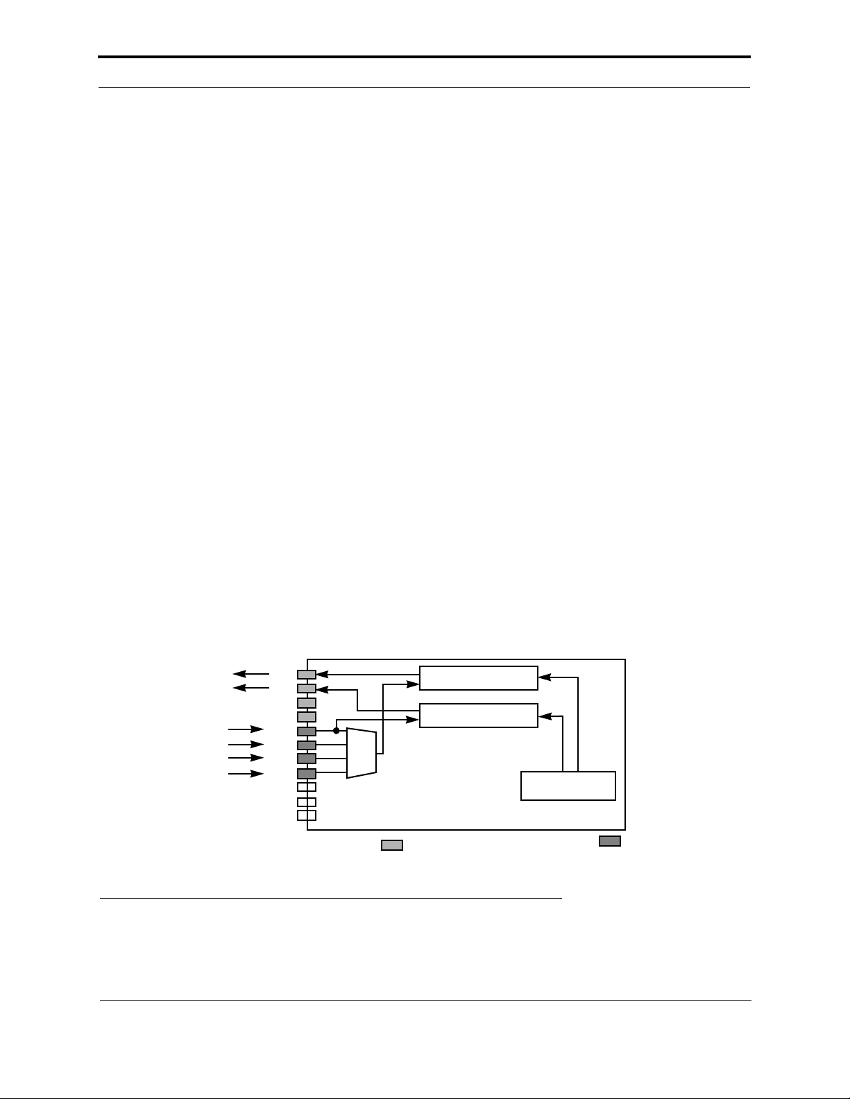
Chapter 3 - Input/Output Interfaces
Overview
The FT 3120 and FT 3150 Smart Transceivers connect to application-specific external hardware via 11 pins, named
IO0-IO10. These pins may be configured in numerous ways to provide flexible input and output functions with
minimal external circuitry. The programming model (Neuron C language) allows the programmer to declare one or
more pins as I/O objects. An I/O object provides programmable access to an I/O driver for a specified on-chip I/O
hardware configuration and a specified input or output waveform definition. The program can then refer to these
objects in io_in and io_out() system calls to perform the actual input/output function during execution of the program.
Certain events are associated with changes in input values. The task scheduler can thus execute associated application
code when these changes occur.
There are 34 different I/O objects available for use with the FT Smart Transceivers. Most I/O Objects are available in
the FT Smart Transceiver system images by default. If an object not included in the default system image is required
by an application, the development tool will link the appropriate objects into available memory space. For FT 3120
Smart Transceiver designs, this means that internal EEPROM space must be used for the additional object. For FT
3150 Smart Transceiver designs, the object will be added to an external flash or ROM region beyond the 16KB space
reserved for the system image.
The FT Smart Transceivers have two 16-bit timer/counters on-chip (see Figure 2.7). The input to timer/counter 1,
also called the multiplexed timer/counter, is selectable among pins IO4 – IO7, via a programmable multiplexer (mux)
and its output may be connected to pin IO0. The input to timer/counter 2, also called the dedicated timer/counter, may
be connected to pin IO4 and its output to pin IO1. The timer/counters are implemented as a 16-bit load register
writable by the CPU, a 16-bit counter, and a 16-bit latch readable by the CPU. The load register and latch are
accessed a byte at a time. No I/O pins are dedicated to timer/counter functions. If, for example, timer/counter 1 is
used for input signals only, then IO0 is available for other input or output functions. Timer/counter clock and enable
inputs may be from external pins, or from scaled clocks derived from the system clock; the clock rates of the two
timer/counters are independent of each other. External clock actions occur optionally on the rising edge, the falling
edge, or both rising and falling edges of the input.
Multiple timer/counter input objects may be declared on different pins within a single application. By calling the
io_select() function, the application can use the first timer/counter to implement up to four different input objects. If a
timer/counter is configured to implement one of the output objects, or is configured as a quadrature input object, then
it can not be reassigned to another timer/counter object in the same application program.
IO0
IO1
IO2
IO3
IO4
IO5
IO6
IO7
IO8
IO9
IO10
20 mA Sink Capability
mux
Timer/Counter 1
Timer/Counter 2
System Clock
Divide Chain
Programmable Pull-Up Capability
Figure 3.1 FT Smart Transceiver Timer/Counter External Connections
32 FT 3120 / FT 3150 Smart Transceiver Data Book
Page 39

Hardware Considerations
Hardware Considerations
Tables 3.1 through 3.5 list the 34 different I/O objects available. Various I/O objects of different types may be used
simultaneously. Figure 3.3 summarizes the pin configuration for each of the I/O objects. For the electrical
characteristics of these pins, refer to the FT 3120 and FT 3150 Smart Transceiver Datasheet. The following sections
contain detailed descriptions of all the I/O objects. The application program may optionally specify the initial values
of digital outputs. Pins configured as outputs may also be read as inputs, returning the value last written. Pins IO4 –
IO7 have optional pull-up current sources that act like pull-up resistors (see Figure 3.1). These are enabled with a
Neuron C compiler directive (#pragma enable_io_pullups). Pins IO0 – IO3 have high sink capability. The others have
standard sink capability. Pins IO0 – IO7 have low-level detect latches. The latency and timing values described
later in this section are typical at 10MHz. The accuracy of these values is ± 10%. Most latency values scale down
at higher input clock rates and scale up at lower input clock rates.
The I/O pull-ups are always enabled during the stack initialization and BIST task. This can cause a problem in some
applications, for example driving a relay. The best solution is to use an I/O that does not have a pull-up. However, if
an I/O with a pull-up must be used, a pull-down resistor could be used to overcome the effects of the pull-up.
Typically, a pull-down in the range of 2.4k to 2.7k is adequate.ΩΩ
FT 3120 / FT 3150 Smart Transceiver Data Book 33
Page 40

Chapter 3 - Input/Output Interfaces
Table 3.1 Summary of Direct I/O Objects
I/O Object Applicable I/O Pins Input/Output Value
Bit Input IO0 – IO10 0, 1 binary data 40
Bit Output IO0 – IO10 0, 1 binary data 40
Byte Input IO0 – IO7 0 – 255 binary data 41
Byte Output IO0 – IO7 0 – 255 binary data 41
Leveldetect Input IO0 – IO7 Logic 0 level detected 43
Nibble Input Any adjacent 4 in IO0 – IO7 0 – 15 binary data 44
Nibble Output Any adjacent 4 in IO0 – IO7 0 – 15 binary data 44
Table 3.2 Summary of Parallel I/O Objects
I/O Object Applicable I/O Pins Input/Output Value
Muxbus I/O IO0 – IO10 Parallel bidirectional port using mul-
tiplexed addressing
Parallel I/O IO0 – IO10 Parallel bidirectional handshaking
port
Table 3.3 Summary of Serial I/O Objects
Page
No.
Page
No.
45
46
I/O Object Applicable I/O Pins Input/Output Value
Bitshift Input Any adjacent pair
(except IO7 + IO8)
Bitshift Output Any adjacent pair
(except IO7 + IO8)
I2C
Magcard Input IO8 + IO9 + (one of IO0 – IO7) Encoded ISO7811 track 2 data
Magtrack1 IO8 + IO9 + (one of IO0 – IO7) Encoded ISO3554 track 1 data
Neurowire I/O IO8 + IO9 + IO10 + (one of IO0 – IO7) Up to 256 bits of bidirectional
Serial Input IO8 8-bit characters 66
Serial Output IO10 8-bit characters 66
Touch I/O IO0 – IO7 Up to 2048 bits of input or output
Wiegand Input Any adjacent pair in IO0 – IO7 Encoded data stream from Wie-
IO8 + IO9 Up to 255 bytes of bidirectional
Up to 16 bits of clocked data 57
Up to 16 bits of clocked data 57
serial data
stream from a magnetic card
reader
stream from a magnetic card
reader
serial data
bits
gand card reader
Page
No.
59
60
62
63
67
69
34 FT 3120 / FT 3150 Smart Transceiver Data Book
Page 41

Hardware Considerations
Table 3.4 Summary of Timer/Counter Input Objects
Page
I/O Object Applicable I/O Pins Input Signal
Dualslope Input IO0, IO1 + (one of IO4 – IO7) Comparator output of the dualslope
converter logic
Edgelog Input IO4 A stream of input transitions 72
Infrared Input IO4 – IO7 Encoded data stream from an infra-
red demodulator
Ontime Input IO4 – IO7 Pulse width of 0.2 µs – 1.678 s 74
Period Input IO4 – IO7 Signal period of 0.2 µs – 1.678 s 75
Pulsecount Input IO4 – IO7 0 – 65,535 input edges during 0.839 s77
No.
71
73
Quadrature Input IO4 + IO5, IO6 + IO7 ± 16,383 binary Gray code transi-
tions
Totalcount Input IO4 – IO7 0 – 65,535 input edges 79
78
Table 3.5 Summary of Timer/Counter Output Objects
Page
I/O Object Applicable I/O Pins Output Signal
Edgedivide Output IO0, IO1 + (one of IO4 – IO7) Output frequency is the input fre-
quency divided by a user-specified
number
Frequency Output IO0, IO1 Square wave of 0.3 Hz to 2.5MHz 81
Oneshot Output IO0, IO1 Pulse of duration 0.2 µs to 1.678 s 83
Pulsecount Output IO0, IO1 0 – 65,535 pulses 84
Pulsewidth Output IO0, IO1 0 – 100% duty cycle pulse train 85
Triac Output IO0, IO1 + (one of IO4 – IO7) Delay of output pulse with respect to
input edge
Triggeredcount Output
IO0, IO1 + (one of IO4 – IO7) Output pulse controlled by counting
input edges
No.
80
86
87
To maintain and provide consistent behavior for external events and to prevent metastability, all 11 I/O pins of the FT
Smart Transceiver, when configured as inputs, are passed through a hardware synchronization block sampled by the
internal system clock. This is always the input clock divided by two (e.g. 10MHz ÷ 2 = 5MHz). For any signal to be
reliably synchronized with a 10MHz input clock, it must be at least 220 ns in duration (see Figure 3.2).
All inputs are software sampled during when statement processing. The latency in sampling is dependent on the I/O
object which is being executed (see I/O timing specification and Neuron C Programmer’s Guide for more
information). These latency values scale inversely with the input clock. Thus, any event that lasts longer than 220 ns
will be synchronized by hardware, but there will be latency in software sampling resulting in a delay detecting the
event. If the state changes at a faster rate than software sampling can occur, then the interim changes will go
undetected.
There are two exceptions to the synchronization block. First, the chip select (CS
) input used in the slave B mode of
the parallel I/O object; this input will recognize rising edges asynchronously (see page 45). Second, the leveldetect
input is latched by a flip flop with a 200ns clock. The leveldetect transition event will be latched, but there will be a
delay in software detection (see page 43). The input timer/counter functions are also different, in that events on the I/
O pins will be accurately measured and a value returned to a register, regardless of the state of the application
processor. However, the application processor may be delayed in reading the register. Consult the Neuron C
Programmer’s Guide for detailed programming information.
FT 3120 / FT 3150 Smart Transceiver Data Book 35
Page 42

Chapter 3 - Input/Output Interfaces
IO_0 – IO_10
Input
t
setup
20 ns
t
hold
0 ns
Internal
System
Clock
Figure 3.2 Synchronization of External Signals
(200 ns pulse
with 10MHz
Input Clock)
36 FT 3120 / FT 3150 Smart Transceiver Data Book
Page 43

I/O Timing Issues
DIRECT
I/O
OBJECTS
Nibble Input, Nibble Output
PARALLEL
I/O
OBJECTS
SERIAL
I/O
OBJECTS
TIMER/COUNTER
OBJECTS
TIMER/
COUNTER
OUTPUT
OBJECTS
Parallel I/O
Bitshift Input, Bitshift Output
INPUT
I/O Pin
Bit Input, Bit Output
Byte Input, Byte Output
Leveldetect Input
Muxbus I/O
Master/Slave A
Slave B
2
I
C I/O
Magcard Input
Magtrack1 Input
Neurowire I/O
Dualslope Input
Master
Slave
Serial Input
Serial Output
Wiegand Input
Edgelog Input
Infrared Input
Ontime Input
Period Input
Pulsecount Input
Quadrature Input
Totalcount Input
Edgedivide Output
Frequency Output
Oneshot Output
Pulsecount Output
Pulsewidth Output
Triac Output
Triggeredcount Output
012345678910
All Pins 0 – 7
Any Four Adjacent Pins
Data Pins 0 – 7
Data Pins 0 – 7
Data Pins 0 – 7
CD CD C
Optional Timeout
Optional Timeout
Optional Chip Select
Optional Timeout
Any Two Pins (Optional Timeout)
Control
Control
Control
012345678910
High Sink
D
4 + 5 6 + 7
Sync Input
Sync Input
Sync Input
Pull Ups
CD
ALS WS RS
R/W HS
CS
A0
R/W
CS
CD
C
CD
CD
CD
CD
D
CD
D
Standard
Notes:
C = Clock, D = Data
2
Bitshift, I
rowire
Timer/Counter 1 Devices
One of:
IO_6 input quadrature
IO_4 input edgelog
IO_0 output [triac | triggeredcount |
IO_0 output [frequency | oneshot |
Or up to four of:
IO_4 input [ontime | period ⎟ pulsec-
IO_5..7 input [ontime | period ⎟
Timer/Counter 2 Devices
One of:
IO_4 input quadrature
IO_4 input edgelog
IO_1 output [triac ⎟ triggeredcount ⎟
IO_1 output [frequency ⎟ oneshot ⎟
IO_4 input [ontime ⎟ period ⎟ pulsec-
C, Magcard, Magtrack, Neu-
edgedivide] sync(IO_4..7)
pulsecount | pulsewidth]
ount ⎟ totalcount ⎟ dualslope ⎟ infrared] mux
pulsecount ⎟ totalcount ⎟ dualslope ⎟ infrared]
edgedivide] sync(IO_4)
pulsecount ⎟ pulsewidth]
ount ⎟ totalcount ⎟ dualslope ⎟ infrared] ded
Figure 3.3 Summary of I/O Objects
I/O Timing Issues
The FT Smart Transceiver I/O timing is influenced by three separate, yet overlapping areas of the overall chip
architecture:
• The scheduler
• The I/O firmware of the object
FT 3120 / FT 3150 Smart Transceiver Data Book 37
Page 44

Chapter 3 - Input/Output Interfaces
• The FT Smart Transceiver hardware
The contribution of the scheduler to the overall timing characteristic is approximately uniform across all 34 I/O
function blocks since its contribution to the overall I/O timing is at a relatively high functional level.
The contribution of firmware and hardware varies from one I/O object to another (e.g., Bit I/O versus Neurowire I/O),
with one area generally being the dominant factor.
Scheduler-Related I/O Timing Information
As part of the FT Smart Transceiver firmware, the scheduler provides an orderly and predictable means to facilitate
the evaluation of user-defined events. The when clause, provided by the Neuron C language, is used to specify such
events. For more information on the operation of the scheduler, refer to the Neuron C Programmer’s Guide.
There is a finite latency associated with the operation of the scheduler. The time required for the scheduler to evaluate
the same when clause in a particular user application code is, to a large extent, a function of the size of the user code,
the total number of when clauses, and the state of the events associated with those when clauses. Therefore, it is
impossible to specify a nominal value for this latency, as each application will have its own distinct behavior under
different circumstances.
The best case latency can be viewed in several ways, each exposing a different aspect of the scheduler operation. A
simple example consists of having an application program consisting of two when clauses, both of which always
evaluate to TRUE, as shown below.
IO_0 output bit testbit;
when (TRUE) {
io_out(testbit, 1);
}
when (TRUE) {
io_out (testbit, 0);
}
Processing of when clauses is done in a round-robin fashion; therefore, the Neuron C code above performs alternating
activation of the IO0 pin in order to isolate and extract the timing parameters associated with the scheduler. The
waveform seen on pin IO0 of the FT Smart Transceiver, as a result of the above code, is shown in Figure 3.4.
38 FT 3120 / FT 3150 Smart Transceiver Data Book
Page 45

IO_out call IO_out call IO_out call
I/O Timing Issues
IO_0
TIME
1st when
clause
t
ww
end-of-loop
processing
begins
2nd when
clause
t
ww
t
sol
1st when
clause
(Not to scale)
Symbol Description Typ @ 10MHz
t
t
ww
sol
when-clause to when-clause latency 940 µs
Scheduler overhead latency (see text) 54 µs
Figure 3.4 when-Clause to when-Clause and Scheduler Overhead Latency
The when-clause to when-clause latency, t
(65 µs latency at 10MHz) and is for an event that always evaluates to TRUE. The actual t
, in this case includes the execution time of one io_out() function
ww
for a given application is
ww
driven by the actual task within the when statement as well as the when event which is evaluated.
The above example not only measures the best-case minimum latency between consecutive when clauses (whose
events evaluate to TRUE), t
shown in Figure 3.4, t
minus t
. This shows that the scheduler overhead latency, or the scheduler end-of-loop latency, occurs just before
ww
ww
, but also reveals that the end-of-loop overhead latency of the scheduler is t
ww
is the off-time period of the output waveform and t
is the on-time of the output waveform,
sol
sol
. As
the execution of the last when clause in the program.
The latency associated with the return from the io_out() function is small, relative to that of the execution of the
function call itself.
NOTE: Some I/O objects suspend application processing until the task is complete. This is because they are
firmware-driven. These are bitshift, Neurowire, parallel, and serial I/O objects, I
2
C, magcard, magtrack, Touch I/O,
and Wiegand. They do not suspend network communication as this is handled by the network processor and the
media access processor.
Firmware and Hardware-Related I/O Timing Information
All I/O updates in the FT Smart Transceiver are performed by the Neuron firmware using system image function
calls.
The total latency for a given function call, from start to end, can be broken down into two separate parts. The first is
due to the processing time required before the actual hardware I/O update (read or write) occurs. The second delay is
associated with the time required to finish the current function call and return to the application program.
Overall accuracy is always related to the accuracy of the CLK1 input of the FT Smart Transceiver. Timing diagrams
are provided for all non-trivial cases to clarify the parameters given.
For more information on the operation of each of the I/O objects, refer to the Neuron C Reference Guide.
FT 3120 / FT 3150 Smart Transceiver Data Book 39
Page 46

Chapter 3 - Input/Output Interfaces
Direct I/O Objects
The timing numbers shown in this section are valid for both an explicit I/O call or an implicit I/O call through a when
clause, and are assumed to be for a FT Smart Transceiver running at 10MHz.
Bit Input/Output
Pins IO0 – IO10 may be individually configured as single-bit input or output ports. Inputs may be used to sense TTLlevel compatible logic signals from external logic, contact closures, and the like. Outputs may be used to drive
external CMOS and TTL level compatible logic, switch transistors and very low current relays to actuate highercurrent external devices such as stepper motors and lights. The high (20mA) current sink capability of pins IO0 – IO3
allows these pins to drive many I/O devices directly (refer to Figure 3.5). Figures 3.6 and 3.7 show the bit input and
bit output latency times, respectively. These are the times from which io_in() or io_out() is called, until a value is
returned. The direction of bit ports may be changed between input and output dynamically under application control.
IO0
IO1
IO2
IO3
IO4
IO5
IO6
IO7
IO8
IO9
IO10
High Current Sink Drivers Optional Pull-Up Re-
IO0
IO1
IO2
IO3
IO4
IO5
IO6
IO7
IO8
IO9
IO10
sistors
Figure 3.5 Bit I/O
WARNING: After a Reset, the FT Smart Transceiver performs a self-test which includes enabling the 104-107 pull-
up resistors. This could cause a positive level change.
40 FT 3120 / FT 3150 Smart Transceiver Data Book
Page 47

Direct I/O Objects
t
ret
END OF
io_in()
INPUT
TIME
START OF
io_in()
t
fin
INPUT PIN
SAMPLED
Symbol Description Typ @ 10MHz
t
fin
t
ret
Function call to sample
IO0 – IO10
Return from function
IO0
IO1
IO2
IO3
IO4
IO5
IO6
IO7
IO8
IO9
IO10
41 µs
19 µs
23.4 µs
27.9 µs
32.3 µs
36.7 µs
41.2 µs
45.6 µs
50 µs
19 µs
23.4 µs
27.9 µs
Figure 3.6 Bit Input Latency Values
OUTPUT
TIME
START OF
io_out()
t
fout
OUTPUT PIN
UPDATED
t
ret
END OF
io_out()
Symbol Description Typ @ 10MH z
t
t
fout
ret
Function call to update
IO3 – IO5
All others
Return from function
IO0 – IO10
69 µs
60 µs
5 µs
Figure 3.7 Bit Output Latency Values
Byte Input/Output
Pins IO0 – IO7 may be configured as a byte-wide input or output port, which may be read or written using integers in
the range 0 to 255. This is useful for driving devices that require ASCII data, or other data, eight bits at a time. For
example, an alphanumeric display panel can use byte function for data, and use pins IO8 – IO10 in bit function for
FT 3120 / FT 3150 Smart Transceiver Data Book 41
Page 48

Chapter 3 - Input/Output Interfaces
control and addressing. See Figures 3.8, 3.9, and 3.10. The IO0 represents the LSB of data. The direction of a byte
port may be changed between input and output dynamically under application control.
IO0
IO1
IO2
IO3
IO4
IO5
IO6
IO7
IO8
IO9
IO10
High Current Sink Drivers Optional Pull-Up Resis-
Figure 3.8 Byte I/O
t
fin
INPUT
TIME
START OF
io_in()
INPUT PIN
SAMPLED
Symbol Description Typ @ 10MHz
t
fin
t
ret
Function call to input sample 24 µs
Return from function 4 µs
t
ret
END OF
io_in()
IO0
IO1
IO2
IO3
IO4
IO5
IO6
IO7
IO8
IO9
IO10
Figure 3.9 Byte Input Latency Values
t
fout
OUTPUT
TIME
START OF
io_out()
OUTPUT PIN
UPDATED
Symbol Description Typ @ 10MHz
t
t
fout
ret
Function call to update 57 µs
Return from function 5 µs
t
ret
Figure 3.10 Byte Output Latency Values
END OF
io_out()
42 FT 3120 / FT 3150 Smart Transceiver Data Book
Page 49
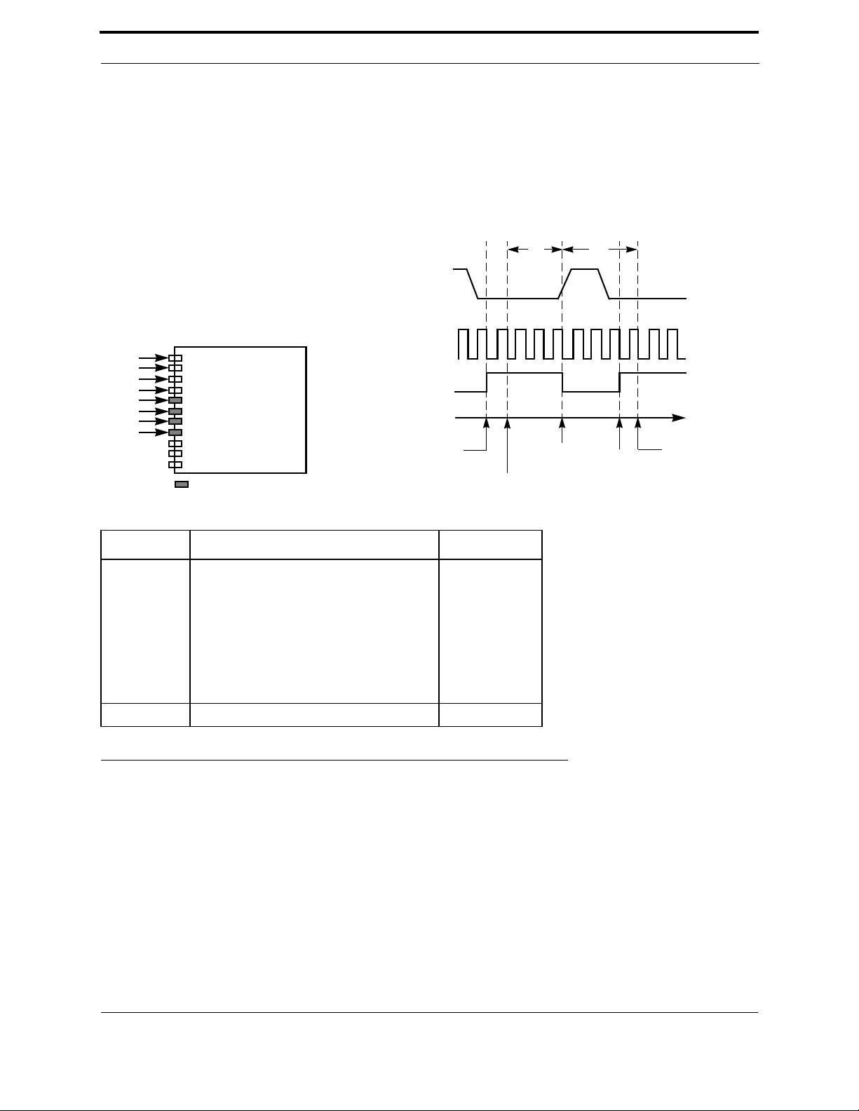
Direct I/O Objects
Leveldetect Input
Pins IO0 – IO7 may be individually configured as leveldetect input pins, which latch a negative-going transition of
the input level with a minimal low pulse width of 200ns, with a FT Smart Transceiver clocked at 10MHz. The
application can therefore detect short pulses on the input which might be missed by software polling. This is useful
for reading devices, such as proximity sensors. This is the only direct I/O object which is latched before it is
sampled. The latch is cleared during the when statement sampling and can be set again immediately after, if another
transition should occur. See Figure 3.11.
INPUT
PIN
200ns
SYSTEM
CLOCK
IO0
IO1
IO2
IO3
IO4
IO5
IO6
IO7
IO8
IO9
IO10
Optional Pull-Up Resistors
(@ 10MHz)
INPUT
LATCH
TIME
1ST NEGATIVE
TRANSITION
IS LATCHED
START OF
io_in()
Symbol Description Typ @ 10MHz
t
fin
t
ret
Function call to sample
IO0
IO1
IO2
IO3
IO4
IO5
IO6
IO7
35 µs
39.4 µs
43.9 µs
48.3 µs
52.7 µs
57.2 µs
61.6 µs
66 µs
Return from function 32 µs
t
fin
INPUT
LATCH
SAMPLED
AND THEN
CLEARED
t
ret
2ND
NEGATIVE
TRANSITION
IS LATCHED
END OF
io_in()
Figure 3.11 Leveldetect Input Latency Values
FT 3120 / FT 3150 Smart Transceiver Data Book 43
Page 50
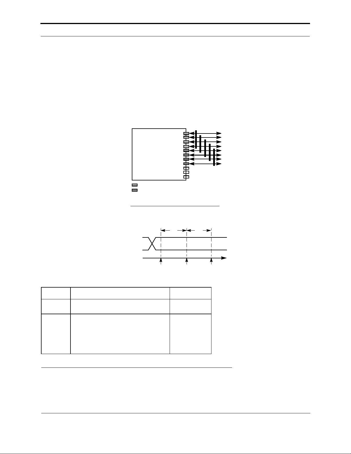
Chapter 3 - Input/Output Interfaces
Nibble Input/Output
Groups of four consecutive pins between IO0 – IO7 may be configured as nibble-wide input or output ports, which
may be read or written to using integers in the range 0 to 15. This is useful for driving devices that require BCD data,
or other data four bits at a time. For example, a 4x4 key switch matrix may be scanned by using one nibble to
generate an output (row select — one of four rows), and one nibble to read the input from the columns of the switch
matrix. See Figures 3.12, 3.13, and 3.14.
The direction of nibble ports may be changed between input and output dynamically under application control (see
the Neuron C Programmer’s Guide). The LSB of the input data is determined by the object declaration and can be any
of the IO0 – IO4 pins.
IO0
IO1
IO2
IO3
IO4
IO5
IO6
IO7
IO8
IO9
IO10
High Current Sink Drivers
Optional Pull-Up Resistors
Figure 3.12 Nibble I/O
t
fin
INPUT
TIME
START OF
io_in()
INPUT PIN
SAMPLED
Symbol Description Typ @ 10MHz
t
fin
t
ret
Function call to sample
IO0 – IO4
Return from function
IO0
IO1
IO2
IO3
IO4
41 µs
18 µs
22.8 µs
27.5 µs
32.3 µs
37 µs
t
ret
Figure 3.13 Nibble Input Latency Values
END OF
io_in()
44 FT 3120 / FT 3150 Smart Transceiver Data Book
Page 51
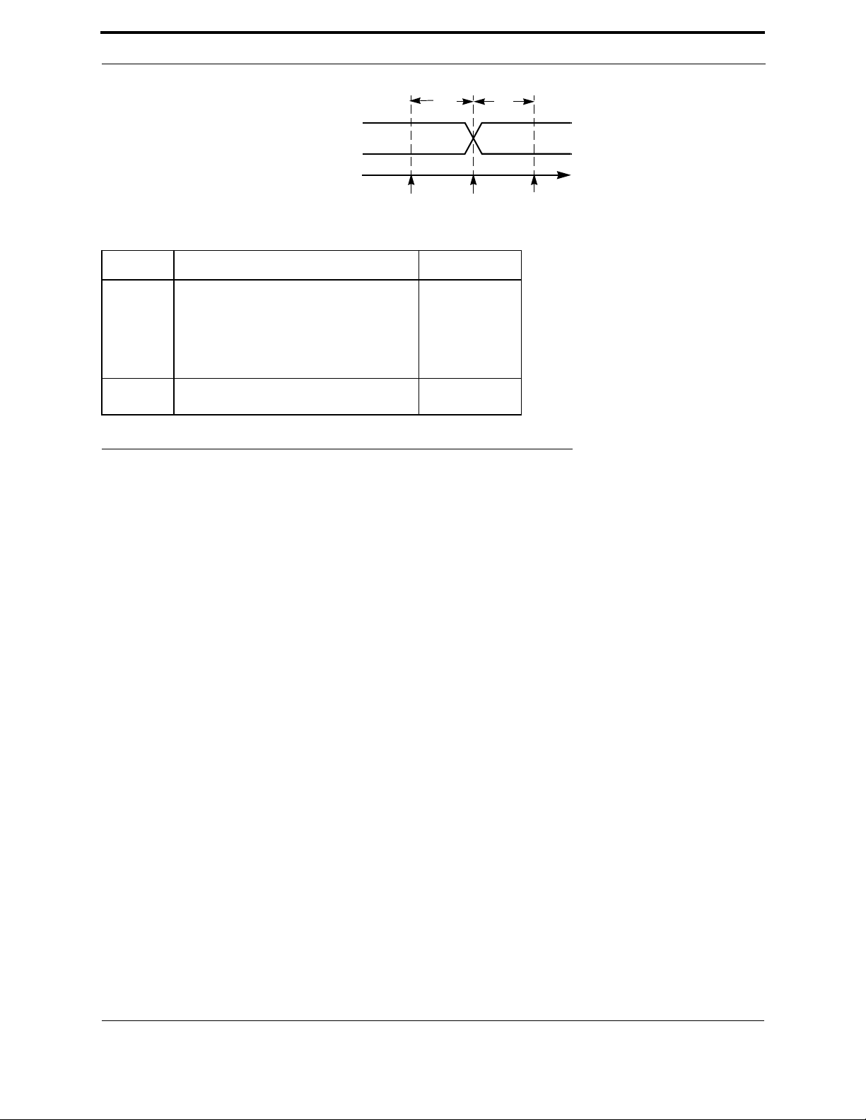
Parallel I/O Objects
t
fout
OUTPUT
TIME
START OF
io_out()
OUTPUT PIN
UPDATED
Symbol Description Typ @ 10MHz
t
t
fout
ret
Function to update
IO0
IO1
IO2
IO3
IO4
Return from function
78 µs
89.8 µs
101.5 µs
113.3 µs
125 µs
IO0 – IO4 5 µs
Figure 3.14 Nibble Output Latency Values
Parallel I/O Objects
t
ret
END OF
io_out()
Muxbus Input/Output
This I/O object provides a means of performing parallel I/O data transfers between the FT Smart Transceiver and an
attached peripheral device or processor (see Figure 3.15). Unlike the parallel input/output object, which makes use of
a token-passing scheme for ensuring synchronization, the muxbus input/output enables the FT Smart Transceiver to
essentially be in control of all read and write operations at all times. This relieves the burden of protocol handling
from the attached device and results in an easier-to-use interface at the expense of data throughput capacity. The data
bus remains in the last state used.
FT 3120 / FT 3150 Smart Transceiver Data Book 45
Page 52
Chapter 3 - Input/Output Interfaces
IO0
IO1
IO2
IO3
IO4
IO5
IO6
IO7
IO8
IO9
IO10
AD0 – AD7
C_ALS
C_WS
C_RS
ADDR/
DATA
C_ALS
(IO8)
C_RS
(IO10)
C_WS
(IO9)
TIME
START OF
io_out()
ADDR
t
t
fout
t
wws
DATA
as
t
was
t
NOTE: Data is latched 4.8 µs after the falling edge of C_RS.
Symbol Description Min Typ Max
t
fout
t
as
t
ahw
t
ahr
t
was
t
wrs
t
wws
t
dws
t
rset
t
whold
t
rhold
t
adrs
t
fin
t
rret
t
wret
io_out() to valid address — 26.4 µs —
Address valid to address strobe — 10.8 µs —
Address hold for write — 4.8 µs —
Address hold for read — 6.6 µs —
Address strobe width — 6.6 µs —
Read strobe width — 10.8 µs —
Write strobe width — 10.8 µs —
Data valid to write strobe — 6.6 µs —
Read setup time 10.8 µs — —
Write hold time 4.2 µs — —
Read hold time 0 µs — —
Address disable to read strobe — 7.2 µs —
io_in() to valid address — 26.4 µs —
Function return from read — 4.2 µs —
Function return from write — 4.2 µs —
t
ahw
t
dws
wret
END OF
io_out()
t
as
t
whold
ADDR
t
adrs
t
fin
START OF
io_in()
DATA
t
rset
t
ahr
t
wrs
END OF
io_in()
t
rhold
t
rret
Figure 3.15 Muxbus I/O Object
Parallel Input/Output
Pins IO0 – IO10 may be configured as a bidirectional 8-bit data and 3-bit control port for connecting to an external
processor. The other processor may be a computer, microcontroller, or another FT Smart Transceiver (for gateway
applications). The parallel interface may be configured in master, slave A, or slave B mode. Typically, two FT Smart
Transceivers interface in master/slave A mode and a FT Smart Transceiver
46 FT 3120 / FT 3150 Smart Transceiver Data Book
interfaces with another microprocessor in
Page 53
Parallel I/O Objects
the slave B configuration, with the other microprocessor as the master. Handshaking is used in both modes to control
the instruction execution, and application processing is suspended for the duration of the transfer (up to 255 bytes/
transfer). Consult the Neuron C Reference Guide for detailed programming instructions.
Upon a reset condition, the master processor monitors the low transition of the handshake (HS) line from the slave,
then passes a CMD_RESYNC (0x5A) for synchronization purposes. This must be done within 0.84 seconds after
reset goes high with a FT Smart Transceiver slave running at 10MHz, to avoid a watchdog reset error condition (see
the Neuron C Programmer’s Guide). The CMD_RESYNC is followed by the slave acknowledging with a
CMD_ACKSYNC (0x07). This synchronization ensures that both processors are properly reset before data transfer
occurs. When interfacing two FT Smart Transceivers, these characters are passed automatically (refer to the flow
table illustrated later in this section). However, when using parallel I/O to interface the FT Smart Transceiver to
another microprocessor, that microprocessor must duplicate the interface signals and characters that are automatically
generated by the parallel I/O function of the FT Smart Transceiver.
For additional information, see the Parallel I/O Interface to the Neuron Chip engineering bulletin.
The timing numbers shown in this section are valid for both an explicit I/O call or an implicit I/O call through a when
clause, and are assumed to be for a FT Smart Transceiver running at 10MHz.
Master/Slave A Mode
This mode is recommended when interfacing two FT Smart Transceivers. In a master/slave A configuration, the
master drives IO8 as a chip select and IO9 to specify a read or write cycle, and the slave drives IO10 as a handshake
(HS) acknowledgment (see Figure 3.16). The maximum data transfer rate is 1 byte per 4 processor instruction cycles,
or 0.6 µs per byte at a 40MHz input clock rate. The data transfer rate scales proportionally to the input clock rate (a
master write is a slave read). Timing for the case where the FT Smart Transceiver is the master (Figure 3.17), refers to
measured output timing at 10MHz. After every byte write or byte read, the HS line is monitored by the master, to
verify the slave has completed processing (when HS = 0) and the slave is ready for the next byte transfer. This is done
automatically in FT Smart Transceiver-to-FT Smart Transceiver (master/slave A mode) data transfers. The HS line
should be pulled up (inactive) with a 10k resistor to ensure proper resynch behavior after the slave resets.
Ω
Slave A timing is shown in Figure 3.18.
IO0
IO1
IO2
IO3
IO4
IO5
IO6
IO7
IO8
IO9
IO10
D0 – D7
CS
R/W
HS
Figure 3.16 Parallel I/O — Master and Slave A
D0 – D7
R/W
CS
HS
IO0
IO1
IO2
IO3
IO4
IO5
IO6
IO7
IO8
IO9
IO10
PARALLEL SLAVE APARALLEL MASTER
FT 3120 / FT 3150 Smart Transceiver Data Book 47
Page 54
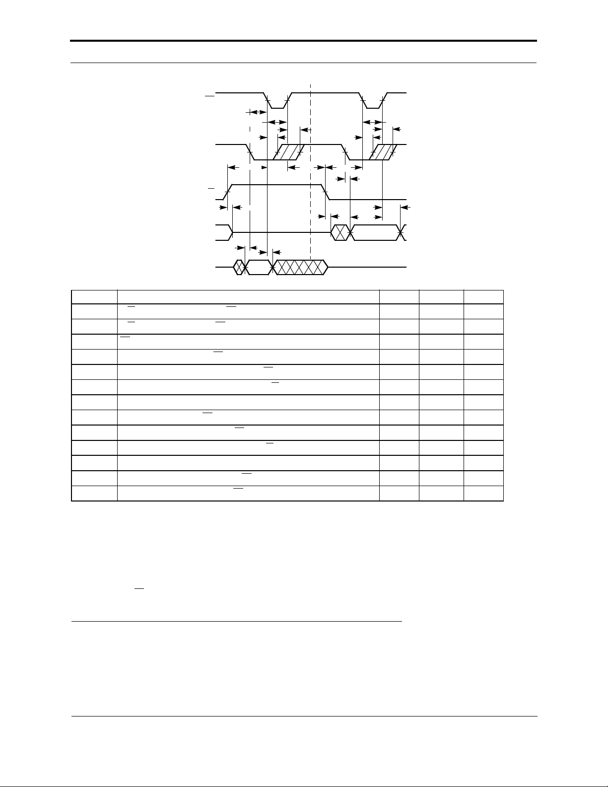
Chapter 3 - Input/Output Interfaces
CS
t
mhscs
t
HS
R/W
DATA OUT
DATA IN
t
mrds
mcspw
t
mhsh
t
mrws
t
mrdz
t
READ CYCLE WRITE CYCLE
mrdh
t
mrwh
t
mwdd
t
mhsv
t
mhsh
t
mrws
t
t
Symbol Description Min Typ Max
t
mrws
t
mrwh
t
mcspw
t
mhsh
t
mhsv
t
mrdz
t
mrds
t
mhscs
t
mrdh
t
mwdd
t
mhsdv
t
mwds
t
mwdh
R/W setup before falling edge of CS 150 ns 3 CLK1 —
R/W hold after rising edge of CS 100 ns — —
CS pulse width 150 ns 2 CLK1 —
HS hold after falling edge of CS 0 ns — —
HS checked by firmware after rising edge of CS 150 ns 10 CLK1 —
Master three-state DATA after rising edge of R/W (Notes 1, 2) — 0 25 ns
Read data setup before falling edge of HS (Note 3) 0 ns — —
HS low to falling edge of CS (Note 4) 2 CLK1 6 CLK1 —
Read data hold after falling edge of CS 0 ns — —
Master drive of DATA after falling edge of R/W (Note 1) 150 ns 2 CLK1 —
HS low to data valid (Note 4) — 50 ns —
Write data setup before rising edge of CS 150 ns 2 CLK1 —
Write data hold after rising edge of CS (Note 6) Note 1 — —
t
mhsdv
mwdh
mwds
t
mcspw
t
mhsv
Notes:
1. Refer to the FT 3120 and FT 3150 Smart Transceiver Datasheet for detailed measurement information.
2. For FT Smart Transceiver-to-FT Smart Transceiver operation, bus contention (t
is present when the token is passed between the master and slave. See Parallel I/O Interface to the Neuron Chip engineering bulletin for fur-
ther information.
3. HS high is used as a slave busy flag. If HS is held low, the maximum data transfer rate is 24 CLK1s (2.4 µs @ 10MHz) per byte. If HS is not
used for a flag, caution should be taken to ensure the master does not initiate a data transfer before the slave is ready.
4. Parameters were added in order to aid interface design with the FT Smart Transceiver.
6. Master will hold output data valid during a write until the Slave device pulls HS low.
7. CLK1 represents the period of the FT Smart Transceiver input clock (100 ns at 10MHz).
8. In a master read, CS
pulsing low acts like a handshake to flag the slave that data has been latched in.
mrdz
, t
) is eliminated by firmware, ensuring that a zero state
sawdd
Figure 3.17 Master Mode Timing
48 FT 3120 / FT 3150 Smart Transceiver Data Book
Page 55

Parallel I/O Objects
CS
HS
R/W
DATA IN
DATA OUT
t
sawds
t
sacspw
t
sarws
t
sawd
t
sawdh
WRITE CYCLE
(MASTER READ)
t
sahsh
t
sarwh
t
sahsv
t
sacspw
t
sahsh
t
sarws
t
sards
t
sardz
READ CYCLE
(MASTER WRITE)
t
sahsv
t
sardh
Symbol Description Min Ty p Max
t
t
t
sacspw
t
t
t
t
t
t
t
t
Notes:
1. Refer to the FT 3120 and FT 3150 Smart Transceiver Datasheet for detailed measurement information.
2. For FT Smart Transceiver-to-FT Smart Transceiver operation, bus contention (t
is present when the token is passed between the master and slave. See Parallel I/O Interface to the Neuron Chip engineering bulletin for further
information.
3. If t
5. CLK1 represents the period of the FT Smart Transceiver input clock (100 ns at 10MHz).
6. In slave A mode, the HS signal is high a minimum of 4 CLK1 periods. The typical time HS is high during consecutive data reads or consecutive
data writes is also 4 CLK1 periods.
R/W setup before falling edge of CS 25 ns — —
sarws
R/W hold after rising edge of CS 0 ns — —
sarwh
CS pulse width 45 ns — —
HS hold after rising edge of CS 0 ns — —
sahsh
HS valid after rising edge of CS — — 50 ns
sahsv
Slave A drive of DATA after rising edge of R/W (Notes 1, 2) 0 ns 5 ns —
sawdd
Write data valid before falling edge of HS 150 ns 2 CLK1 —
sawds
Write data valid after rising edge of CS 150 ns
sawdh
Slave A three-state DATA after falling edge of R/W (Note 1) — — 50 ns
sardz
Read data setup before rising edge of CS 25 ns — —
sards
Read data hold after rising edge of CS 10 ns — —
sardh
, t
mrdz
sawdd
< 150 ns, then t
sarwh
sawdh
= t
sarwh
.
(Note 3)
) is eliminated by firmware, ensuring that a zero state
2 CLK1 —
Figure 3.18 Slave A Mode Timing
The following is a pair of example programs that transfer data in a parallel I/O master/slave A configuration. The
code is for two LonBuilder emulators hardwired as shown in Figure 3.16. The master program writes the test_data to
the input bufferof the slave (as the master owns the token after reset and has the first option to write on the bus) and
the slave then outputs data to the input buffer of the master. The buffers can be viewed through the LonBuilder
debugger to verify the transfer was complete. The master transmits [5,1,1,1,1,1] to the slave and the slave transmits
[7,1,2,3,4,5,6,7,0,0,0,0,0,0] to the master. The first byte indicates the number of bytes being passed; the following
non-zero valued bytes in this example are the actual data transferred. The remaining length of the array, if any, is
FT 3120 / FT 3150 Smart Transceiver Data Book 49
Page 56

Chapter 3 - Input/Output Interfaces
filled with 0s. The master program writes once to the slave and reads once from the slave. To implement continuous
writes and reads, add an io_out_request() function call after the io_in() function call in the master program.
/* This is the master program. After reset, the buffer is filled with 1s and then the
buffer is written to the slave. The master then reads the slave’s buffer. The master’s
output buffer should contain [5,1,1,1,1,1]; the input buffer should contain
[7,1,2,3,4,5,6,7,0,0,0,0,0,0].
*/
IO_0 parallel master parallel_bus;
#define TEST_DATA 1 // data to be written in output buffer
#define MAX_IN 13 // maximum length of input data expected
#define OUT_LEN 5 // output length can be equal to or less than the
// max
#define MAX_OUT 5 // maximum array length
struct parallel_out // output structure
{
unsigned int len; // actual length of data to be output
unsigned int buffer[MAX_OUT]; // array setup for max length of
// data to be output
}p_out; // output structure name
struct parallel_in // input structure
{
unsigned int len; // actual buffer length to be input
unsigned int buffer[MAX_IN]; // maximum input array
}p_in; // input structure name
unsigned int i;
when (reset)
{
p_out.len=OUT_LEN; // assign output length
for(i=0; i<OUT_LEN; ++i) // fill output buffer with 1s
p_out.buffer[i]=TEST_DATA;
io_out_request(parallel_bus); // request to output buffer
}
when (io_out_ready(parallel_bus))
{
io_out(parallel_bus, &p_out); // output buffer when slave is ready
}
when (io_in_ready(parallel_bus))
{
p_in.len=MAX_IN; // declare the maximum input
// buffer acceptable
io_in(parallel_bus, &p_in); // store input data in buffer
} // end of program
50 FT 3120 / FT 3150 Smart Transceiver Data Book
Page 57

Parallel I/O Objects
/* This is the slave program. After reset, the output buffer is filled with data and
then the slave reads from the master. The slave then writes to the master. The slave’s
input buffer should contain [5,1,1,1,1,1]; the output buffer should contain
[7,1,2,3,4,5,6,7,0,0,0,0,0,0].
*/
IO_0 parallel slave parallel_bus;
#define MAX_IN 5 // maximum length of input data expected
#define OUT_LEN 7 // output length can be equal to or less than the
// max
#define MAX_OUT 13 // maximum array length
struct parallel_out // output structure
{
unsigned int len; // actual length of data to be output
unsigned int buffer[MAX_OUT]; // array setup for max length of data
// to be output
}p_out; // output structure name
struct parallel_in // input structure
{
unsigned int len; // actual length of buffer to be
// input
unsigned int buffer[MAX_IN]; // maximum input array
}p_in; // input structure name
unsigned int i;
when (reset)
{
p_out.len=OUT_LEN; // assign output length
for(i=0; i<OUT_LEN; ++i) // fill output buffer with 1s
p_out.buffer[i]=i+1;
}
when (io_out_ready(parallel_bus))
{
io_out(parallel_bus, &p_out); // output buffer
}
when (io_in_ready(parallel_bus))
{
p_in.len=MAX_IN; // declare the maximum input buffer
// acceptable
io_in(parallel_bus, &p_in); // store input data in buffer
io_out_request(parallel_bus); // request to output buffer
} // end of program
Debugging the Above Programs: If a watchdog timeout occurs on either LonBuilder emulator, simultaneously reset
the two emulators using the reset pushbutton switches on the face of the emulators. Both JP1 and JP2 on the emulator
boards should be disconnected for this application.
Slave B Mode
The slave B mode is recommended for interfacing a FT Smart Transceiver acting as the slave to another
microprocessor acting as the master. When configured in slave B mode, the FT Smart Transceiver accepts IO8 as a
chip select and IO9 to specify whether the master will read or write, and accepts IO10 as a register select input. When
CS
is asserted and either IO10 is low or IO10 is high and R/W is low, pins IO0 – IO7 form the bidirectional data bus.
When IO10 is high, R/W
FT 3120 / FT 3150 Smart Transceiver Data Book 51
is high, and CS is asserted, IO0 is driven as the HS acknowledgment signal to the master.
Page 58

Chapter 3 - Input/Output Interfaces
The FT Smart Transceiver may appear as two registers in the address space of the master; one of the registers being
the read/write data register, and the other being the read-only status register. Therefore, reads by the master to an odd
address access the status register for handshaking acknowledgments and all other reads or writes access the data
register for I/O transfers. The LSB of the control register, which is read through pin IO0, is the HS bit. The master
reads the HS bit after every master read or write. The D0/HS line should be pulled up (inactive) with a 10k
Ω
resistor to ensure proper resynch behavior after resets.
When acting as a slave to a different microprocessor, the FT Smart Transceiver slave B mode handles all handshaking
and token passing automatically. However, the master microprocessor must read the HS bit after each transaction and
must also internally track the token passing. This mode is designed for use with a master processor that uses memorymapped I/O, as the LSB of the address bus of the master is typically connected to the IO10 pin of the FT Smart
Transceiver. This is illustrated in Figures 3.19 and 3.20.
READ ONLY
STATUS REGISTER
HS
X
X
X
X
X
X
X
= 1
R/W
IO10 = 1
READ/WRITE
DATA REGISTER
R /W = 0
IO10 = 1
D0
D1
D2
D3
D4
D5
D6
D7
R /W = 0 OR 1
OR
IO10 = 0
HS/D0 – D7
CS
R/W
A0
D0/HS
D1
D2
D3
D4
D5
D6
D7
IO0
IO1
IO2
IO3
IO4
IO5
IO6
IO7
IO8
IO9
IO10
SLAVE B
Figure 3.19 Parallel I/O Master/Slave B (FT 3120/FT 3150 Smart Transceiver
as Memory-Mapped I/O Device)
Token Passing
Virtual token passing is implemented to eliminate the possibility of data bus contention. The token is owned by the
master after synchronization and is passed between the master and slave devices. After each data transfer is
completed, the token owner writes an end of message (EOM) (0x00) to indicate that the transfer is complete. The
EOM is never read. Instead, “processing the EOM” indicates passing of the token. Token passing can be achieved by
executing either a data packet or a NULL transfer. Only the owner of the token can write to the bus. Therefore, when
the master performs two writes of data (1 – 255 bytes each) a dummy read cycle (NULL character = 0x00) must be
inserted between them in order to pass the token. Token passing is executed automatically in a FT Smart Transceiverto-FT Smart Transceiver interface. Refer to section , Data Transferring, for master/slave flow transactions.
52 FT 3120 / FT 3150 Smart Transceiver Data Book
Page 59

Parallel I/O Objects
Handshaking
Handshaking allows the master to monitor the slave between every byte transfer, ensuring that both processors are
ready for the byte to be transferred. If the master owns the token, the master waits for the HS from the slave before
writing data to the bus. If the slave owns the token, the master monitors the low transition of the HS before reading
the bus. In master or slave A mode, the FT Smart Transceiver HS line is pin IO10. In slave B mode, the FT Smart
Transceiver HS bit is monitored on IO0 which corresponds to the least significant data bit of the status register.
FT 3120 / FT 3150 Smart Transceiver Data Book 53
Page 60

Chapter 3 - Input/Output Interfaces
MASTER CS
t
sbcspw
t
sbah
MASTER A0
MASTER R/W
MASTER
DATA OUT
SLAVE
DATA OUT
t
sbas
t
sbrws
t
sbwdv
WRITE CYCLE
(MASTER READ)
t
sbrwh
LATCH
t
sbwdz
t
sbwdh
t
sbrws
t
sbrds
READ CYCLE
(MASTER WRITE)
Symbol Description Min Ty p Max
t
sbrws
t
sbrwh
t
sbcspw
t
sbas
t
sbah
t
sbwdv
t
sbwdh
t
sbwdz
t
sbrds
t
sbrdh
Notes:
1. The slave B write cycle (master read) CS pulse width is directly related to the slave B write data valid parameter and master read setup parameter. To calculate the write cycle CS duration needed for a special application use:
t
sbcspw
Refer to the master’s specification data book for the master read setup parameter. The slave read cycle minimum CS pulse width = 50 ns.
2. Refer to the FT 3120 and FT 3150 Smart Transceiver Datasheet for detailed measurement information.
3. The data hold parameter, t
to the traditional data invalid levels.
4. In a slave B write cycle the timing parameters are the same for a control register (HS) write as for a data write.
5. Special applications: Both the state of CS
W
line can be used with no changes to the hardware. In other words, if CS is held low during a slave B write cycle, a positive pulse (low to high
to low) on R/W
t
sbwdv
as the CS
data transitions. This application may be helpful if the master has separate read and write signals but no CS
ensure the bus is free before transfers to avoid bus contention.
R/W setup before falling edge of CS
FT 3120 and FT 3150 Smart Transceivers 0 ns — —
R/W hold after rising edge of CS 0 ns — —
CS pulse width Note 1 — —
A0 setup to falling edge of CS 10 ns — —
A0 hold after rising edge of CS 0 ns — —
CS to write data valid — — 50 ns
Write data hold after rising edge of CS (Notes 2, 3) 0 ns 30 ns —
CS rising edge to Slave B release data bus (Note 2) — — 50 ns
Read data setup before rising edge of CS 25 ns — —
Read data hold after rising edge of CS 10 ns — —
= t
+ master’s read data setup before rising edge of CS
sbwdv
, is measured to the disable levels shown in the FT 3120 and FT 3150 Smart Transceiver Datasheet, rather than
sbwdh
and R/W determine a slave B write cycle. If CS can not be used for a data transfer, then toggling the R/
(redefined R/W to write data valid). Likewise, the falling edge of R/W causes slave B to release the data bus with the same timing limits
can execute a data transfer. The low to high transition on R/W causes slave B to drive data with the same timing parameters as
rising edge in t
. This scenario is only true for a slave B write cycle and is not applicable to a slave B read cycle or any slave A
sbwdz
t
sbcspw
t
sbrdh
signal. Caution must be taken to
Figure 3.20 Slave B Mode Timing
Data Transferring
The data transfer operation between the master and the slave is accomplished through the use of a virtual write tokenpassing protocol. The write token is passed alternatively between the master and the slave on the bus in an infinite
ping-pong fashion. The owner of the token has the option of writing a series of data bytes, or alternatively, passing the
write token without any data. Figure 3.21 illustrates the sequence of operations for this token passing protocol.
54 FT 3120 / FT 3150 Smart Transceiver Data Book
Page 61

MASTER
HAS
TOKEN
FT SMART
TRANSCEIVERS
Parallel I/O Objects
MASTER
SLAVE
HAS
TOKEN
SLAVE
WRITE
DATA
WRITE
DATA
PAS S
TOKEN
PAS S
TOKEN
CMP_
RESYNC
CMP_ACK
RESYNC
Figure 3.21 Handshake Protocol Sequence Between the Master and the Slave
Once in possession of the write token, the device (FT Smart Transceiver or a host processor) can transfer up to 255
bytes of data. The stream of data bytes is preceded by the command and length bytes. The token holder keeps
possession of the token until all data bytes have been written, after which the token is passed to the attached device.
The same process may now be repeated by the other side or, alternatively, the token can be passed back without any
data. The timing relationship between the various FT Smart Transceiver signals involved in this process is shown in
the following timing diagrams.
Resynchronization Procedure: The following procedure applies to master/slave A and master/slave B
configuration. The master initiates the resynchronization with a RESYNC (0x5A) command, and the slave
acknowledges with an ACKSYNC (0x07). If the slave does not respond, the master continues to send the RESYNC
until the slave responds correctly.
MASTER SLAVE
(Owns Token)
Write RESYNC // master initiates resynchronization (0x5A)
Read RESYNC
Write EOM // end of message (EOM=0x00)
Process EOM
Write ACKSYNC // slave acknowledges resynching (0x07)
Read ACKSYNC
Write EOM
Process EOM // master owns token when reset
(Owns Token)
Master writes buffer to slave: Enter RD/_WR=0.
MASTER SLAVE
(Owns Token)
Write XFER // master has data to write (XFER=0x01)
Read XFER
Write (length) // length=number of bytes of data
FT 3120 / FT 3150 Smart Transceiver Data Book 55
Page 62

Chapter 3 - Input/Output Interfaces
Read (length)
Write (data_0) // master begins data transfer to slave
Read (data_0)
..
..
..
Write (data_n) // last byte of data to be transferred
Read (data_n)
Write EOM // end of data transfer (EOM=0x00)
Process EOM// exchange token
(Owns Token)
Slave writes buffer to master: Enter RD/_WR=1.
MASTER SLAVE
(Owns Token)
Write XFER // slave has data to write (XFER=0x01)
Read XFER
Write (length) // length=number of bytes of data
Read (length)
Write (data_0) // slave begins writing data to master
Read (data_0)
..
..
..
Write (data_n) // last byte of data to be transferred
Read (data_n)
Write EOM // end of data transfer
Process EOM // exchange token
(Owns Token)
Master passes token to slave: Entry same as when master writes buffer to slave.
MASTER SLAVE
(Owns Token)
Write NULL // master has no data to send to slave
Read NULL // NULL=0x00
Write EOM // end of message (EOM=0x00)
Process EOM // exchange token
(Owns Token)
Slave passes token to master: Entry same as when slave writes buffer master.
MASTER SLAVE
(Owns Token)
Write NULL // slave has no data to send to the master
Read NULL // NULL=0x00
Write EOM // end of message (EOM=0x00)
Process EOM // exchange token
(Owns Token)
56 FT 3120 / FT 3150 Smart Transceiver Data Book
Page 63

Serial I/O Objects
Serial I/O Objects
The timing numbers shown in this section are valid for both an explicit I/O call or an implicit I/O call through a when
clause, and are assumed to be for a FT Smart Transceiver running at 10MHz.
Bitshift Input/Output
Pairs of adjacent pins may be configured as serial input or output lines. The first pin of the pair can be IO0-IO6, IO8,
or IO9, and is used for the clock (driven by the FT Smart Transceiver). The adjacent higher-numbered I/O pin is then
used for up to 16 bits of serial data. The data rate may be configured as 1kbps, 10kbps, or 15kbps at a 10MHz input
clock rate. The data rate scales proportionally to the input clock rate, for example: 4kbps, 40kbps, or 60kbps at a
40MHz input clock rate. The active clock edge may be specified as either rising or falling. This object is useful for
transferring data to external logic employing shift registers. This function suspends application processing until the
operation is complete. See Figures 3.22, 3.23, and 3.24.
IO0
IO1
IO2
IO3
IO4
IO5
IO6
IO7
IO8
IO9
IO10
BITSHIFT OUTPUT
Clk
Data
Clk
Data
Clk
Data
Clk
Data
Clk
Data
BITSHIFT INPUT
IO0
IO1
IO2
IO3
IO4
IO5
IO6
IO7
IO8
IO9
IO10
Clk
Data
Clk
Data
Clk
Data
Clk
Data
Clk
Data
Figure 3.22 Bitshift I/O Examples
For bitshift input, the clock output is deasserted (to the inactive level) at the same time as the start of the first bit of
data. For bitshift output, the clock output is initially inactive prior to the first bit of data (unless overridden by a bit
output overlay).
FT 3120 / FT 3150 Smart Transceiver Data Book 57
Page 64

Chapter 3 - Input/Output Interfaces
OUTPUT
CLOCK
DATA IN
t
t
hold
fin
INPUT SAMPLED
t
aet
t
tae
t
ret
START OF
io_in()
Active clock edge assumed to be positive in the above
diagram
END OF
io_in()
Symbol Description Typ @ 10MHz
t
fin
t
ret
t
hold
t
aet
t
tae
f Clock frequency = 1/(t
Function call to first edge 156.6 µs
Return from function 5.4 µs
Active clock edge to sampling of input data
15 kbps bit rate
10 kbps bit rate
1 kbps bit rate
9 µs
40.8 µs
938.2 µs
Active clock edge to next clock transition
15 kbps bit rate
10 kbps bit rate
1 kbps bit rate
31.8 µs
63.6 µs
961 µs
Clock transition to next active clock edge
15 kbps bit rate
10 kbps bit rate
1 kbps bit rate
15 kbps bit rate
10 kbps bit rate
1 kbps bit rate
aet
+ t
tae
)
14.4 µs
14.4 µs
14.4 µs
21.6 kHz
12.8 kHz
1.03 kHz
Figure 3.23 Bitshift Input Latency Values
58 FT 3120 / FT 3150 Smart Transceiver Data Book
Page 65
OUTPUT
CLOCK
DATA OUT
Serial I/O Objects
t
setup
t
fin
t
aet
t
tae
t
ret
START OF
io_in()
Active clock edge assumed to be positive in the above
diagram
END OF
io_in()
Symbol Description Typ @ 10MHz
t
fin
t
ret
t
setup
t
aet
t
tae
f Clock frequency = 1/(t
Function call to first data out stable
16-bit shift count
1-bit shift count
185.3 µs
337.6 µs
Return from function 10.8 µs
Data out stable to active clock edge
15 kbps bit rate
10 kbps bit rate
1 kbps bit rate
10.8 µs
10.8 µs
10.8 µs
Active clock edge to next clock transition
15 kbps bit rate
10 kbps bit rate
1 kbps bit rate
10.2 µs
42 µs
939.5 µs
Clock transition to next active clock edge
15 kbps bit rate
10 kbps bit rate
1 kbps bit rate
15 kbps bit rate
10 kbps bit rate
1 kbps bit rate
aet
+ t
tae
)
34.8 µs
34.8 µs
34.8 µs
22 kHz
13 kHz
1.02 kHz
Figure 3.24 Bitshift Output Latency Values
I2C Input/Output
This I/O object is used to interface the FT Smart Transceiver to any device which adheres to the Philips
Semiconductor Inter-Integrated Circuit (I
being the serial clock (SCL) and IO9 the serial data (SDA). These I/O lines are operated in the open-drain mode in
order to accommodate the special requirements of the I
additional external components are necessary for interfacing the FT Smart Transceiver to an I
Up to 255 bytes of data may be transferred at a time. At the start of all transfers, a right-justified 7-bit I
argument is sent out on the bus immediately after the I
For more information on this protocol, refer to the Philips Semiconductor I
FT 3120 / FT 3150 Smart Transceiver Data Book 59
2
C) bus protocol. The FT Smart Transceiver is always the master, with IO8
2
C protocol. With the exception of two pull-up resistors, no
2
C device.
2
C address
2
C “start condition.”
2
C documentation.
Page 66

Chapter 3 - Input/Output Interfaces
IO0
IO1
IO2
IO3
IO4
IO5
IO6
IO7
IO8
IO9
IO10
Clock
Serial Data
SDA
SCL
TIME
t
dch
t
chcl
t
chd
t
dcl
INPUT DATA
SAMPLED
BIT TRANSFER TIMING
t
cld
t
clch
SDA
SCL
TIME
START OF
io_in() OR
io_out()
t
start
t
f
t
cla
START AND STOP TIMING
Parameter Description Min Typ Max
t
t
t
t
t
t
t
t
t
t
t
f
start
cla
cld
dch
chcl
chd
dcl
clch
stop
ret
I/O call to start condition
io_in()
io_out()
—
—
54.6 µs
43.4 µs
End of start condition
io_in()
io_out()
5.4 µs
5.4 µs
—
—
End of start to start of address
io_in()
io_out()
24.0 µs
24.0 µs
—
—
SCL low to data for io_out() 24.6 µs — —
Data to SCL high for io_out() 7.2 µs — —
Clock high to clock low for io_out() 12.6 µs — —
SCL high to data sampling for io_in() 13.2 µs — —
Data sample to SCL low for io_in() 7.2 µs — —
Clock low to clock high for io_in() 24.0 µs — —
Clock high to data
io_in()
io_out()
12.6 µs
12.6 µs
—
—
SDA high to return from function
io_in()
io_out()
—
—
—
—
—
—
—
—
—
—
—
—
4.2 µs
4.2 µs
t
stop
t
ret
END OF
io_in() OR
io_out()
Figure 3.25 I2C I/O Object
Magcard Input
This I/O object is used to transfer synchronous serial data from an ISO 7811 Track 2 magnetic stripe card reader in
real time. The data is presented as a data signal input on pin IO9, and a clock, or a data strobe, signal input on pin IO8.
The data on pin IO9 is clocked on or just following the falling (negative) edge of the clock signal on IO8, with the
60 FT 3120 / FT 3150 Smart Transceiver Data Book
Page 67

Serial I/O Objects
LSB first. In addition, any one of the pins IO0 – IO7 may be used as a timeout pin to prevent lockup in case of
abnormal abort of the input bit stream during the input process.
Up to 40 characters may be read at one time. Both the parity and the Longitudinal Redundancy Check (LRC) are
checked by the FT Smart Transceiver.
IO0
IO1
IO2
DATA
(IO9)
CLOCK
(IO8)
TIMEOUT
t
setup
IO3
IO4
IO5
IO6
IO7
IO8
IO9
IO10
t
hold
t
clk
t
low
t
high
Timeout
Clock
Serial Data
t
wto
t
ret
END OF
io_in()
t
tret
TIME
START OF
io_in()
t
fin
Symbol Description Min Ty p Max
t
fin
t
hold
t
setup
t
low
t
high
t
wto
t
clk
t
tret
t
ret
Function call to first clock input — 45.0 µs —
Data hold 0 µs — —
Data setup 0 µs — —
Clock low width 60 µs — —
Clock high width 60 µs — —
Width of timeout pulse 60 µs — —
Clock period 120 µs — —
Return from timeout 21.6 µs — 81.6 µs
Return from function — — 301.8 µs
Figure 3.26 Magcard Input Object
A FT Smart Transceiver operating at 10MHz can process a bit rate at up to 8334 bits/second (of a bit density of 75
bits/inch). This equates to a card velocity of 111 inches/second. Most magnetic card stripes contain a 15-bit sequence
of zero data at the start of the card, allowing time for the application to start the card reading function. At 8334 bits/
second, this period is about 1.8 ms. If the scheduler latency is greater than the 1.8 ms value, the io_in() function
will miss the front end of the data stream. The bit rate processing capability scales with input clock rate. For example:
the bit rate may be up to 33,336 bps at 40MHz.
FT 3120 / FT 3150 Smart Transceiver Data Book 61
Page 68
Chapter 3 - Input/Output Interfaces
Magtrack1 Input
This input object type is used to read synchronous serial data from an ISO3554 magnetic stripe card reader. The data
input is on pin IO9, and the clock, or data strobe, is presented as input on pin IO8. The data on pin IO9 is clocked in
just following the falling edge of the clock signal on IO7, with the LSB first.
IO0
IO1
IO2
SDA
(IO9)
CLOCK
(IO8)
t
t
setup
hold
IO3
IO4
IO5
IO6
IO7
IO8
IO9
IO10
t
high
Timeout
Clock
Serial Data
t
TIMEOUT
TIME
START OF
io_in()
low
t
fin
t
clk
t
Symbol Description Min Typ Max
t
fin
t
hold
t
setup
t
low
t
high
t
wto
t
clk
t
tret
t
ret
Function call to first clock input — 45.0 µs —
Data hold t
low
— t
clk
Data setup 0 µs — —
Clock low width 31 µs — —
Clock high width 31 µs — —
Width of timeout pulse 60 µs — —
Clock period 138 µs — —
Return from timeout 21.6 µs — 81.6 µs
Return from function — — 301.8 µs
t
wto
ret
t
tret
END OF
io_in()
Figure 3.27 Magtrack1 Input Object
The minimum period for the entire bit cycle (t
times should be such that the data is stable for the duration of t
62 FT 3120 / FT 3150 Smart Transceiver Data Book
) is greater than the sum of t
clk
.
low
low
and t
high
. The t
setup
and t
hold
Page 69
Serial I/O Objects
Data are recognized in the IATA format as a series of 6-bit characters plus an even parity bit per character. The
process begins when the start sentinel (hex 05) is recognized, and continues until the end sentinel (0x0F) is
recognized. No more than 79 characters, including the 2 sentinels and the LRC character, will be read. The data is
stored as right-justified bytes in the buffer space pointed to by the buffer pointer argument in the io_in()
function with the parity stripped, and includes the start and end sentinels. This buffer should be 78 bytes long.
The magtrack1 input object optionally uses one of the I/O pins IO0 – IO7 as a timeout/abort pin. Use of this feature is
suggested since the io_in() function will update the watchdog timer during clock wait states, and could
result in a lockup if the card were to stop moving in the middle of the transfer process. If a logic 1 level is
detected on the I/O timeout pin, the io_in() function will abort. This input can be a oneshot timer counter
output, an R/C circuit, or a DATA_VALID
signal from the card reader.
A FT Smart Transceiver with a clock rate of 10MHz can process an incoming bit rate of up to 7246 bits/second when
the strobe signal has a 1/3 duty cycle (t
= 46 µs, t
high
= 92 µs). At a bit density of 210 bits/inch, this translates
low
to a card speed of 34.5 inches/second. The bit rate processing capability scales with FT Smart Transceiver
input clock rate, for example: bit rate up to 28,984bps at 40MHz.
Neurowire (SPI Interface) Input/Output Object
The Neurowire object implements a full-duplex synchronous transfer of data to some peripheral device. It can operate
as the master (drive a clock out) or as the slave (accept a clock in). In both master and slave modes, up to 255 bits of
data may be transferred at a time. The Neurowire I/O suspends application processing until the operation is
completed. The Neurowire object is useful for external devices, such as A/D, D/A converters, and display drivers
incorporating serial interfaces that conform with the Motorola SPI or National Semiconductor Microwave
interfaces. See Figure 3.28.
TM
IO0
IO1
IO2
IO3
IO4
IO5
IO6
IO7
IO8
IO9
IO10
Select
Clock
Data Out
Data In
Timeout
Clock
Data Out
Data In
IO0
IO1
IO2
IO3
IO4
IO5
IO6
IO7
IO8
IO9
IO10
Neurowire SLAVENeurowire MASTER
Figure 3.28 Neurowire I/O
Neurowire Master Mode
In Neurowire master mode, pin IO8 is the clock (driven by the FT Smart Transceiver), IO9 is the serial data output,
and IO10 is the serial data input. Serial data is clocked out on pin IO9 at the same time as data is clocked in from pin
IO10. Data is clocked by the rising edge of the clock signal by default. The clockedge(-) keyword changes the active
edge of the clock to negative. In addition, one or more of the IO0 – IO7 pins may be used as a chip select, allowing
multiple Neurowire devices to be connected on a three-wire bus. The clock rate may be specified as 1kbps, 10kbps, or
20kbps at an input clock rate of 10MHz; these scale proportionally with input clock, for example: 4kbps, 40kbps, or
80kbps at an input clock rate of 40MHz. See Figure 3.29.
FT 3120 / FT 3150 Smart Transceiver Data Book 63
Page 70
Chapter 3 - Input/Output Interfaces
t
t
setup
CLOCK
DATA OUT
DATA IN
CLOCK
SELECT
START OF
io_in() OR io_out()
t
t
cs_clock
t
high
fin
hold
INPUT SAMPLED
Parameter Description Ty p
t
fin
t
ret
t
hold
Function call to CS active 69.9 µs
Return from function 7.2 µs
Active clock edge to sampling of input data
20 kbps bit rate
10 kbps bit rate
1 kbps bit rate
t
high
Period, clock high (active clock edge = 1)
20 kbps bit rate
10 kbps bit rate
1 kbps bit rate
t
low
t
setup
t
cs clock
t
clock cs
f Clock frequency = 1/(t
Period, clock low (active clock edge = 1) 33.0 µs
Data output stable to active clock edge 5.4 µs
Select active to first active clock edge 91.2 µs
Last clock transition to select inactive 81.6 µs
+ t
low
)
high
20 kbps bit rate
10 kbps bit rate
1 kbps bit rate
t
low
io_in() OR io_out()
11.4 µs
53.4 µs
960.6 µs
25.8 µs
67.8 µs
975.0 µs
17.0 kHz
9.92 kHz
992 Hz
t
clock_cs
t
ret
END OF
Figure 3.29 Neurowire (SPI) Master Timing
Neurowire Slave Mode
In Neurowire slave mode, pin IO8 is the clock (driven by the external master), IO9 is the serial data output, and IO10
is the serial data input. Serial data is clocked out on pin IO9 at the same time as data is clocked in from pin IO10. Data
is clocked by the rising edge of the clock signal (default), which may be up to 18kbps at 10MHz. This data rate scales
with FT Smart Transceiver input clock rate, for example: 72kbps at 40MHz. The clockedge(-) keyword changes
64 FT 3120 / FT 3150 Smart Transceiver Data Book
Page 71
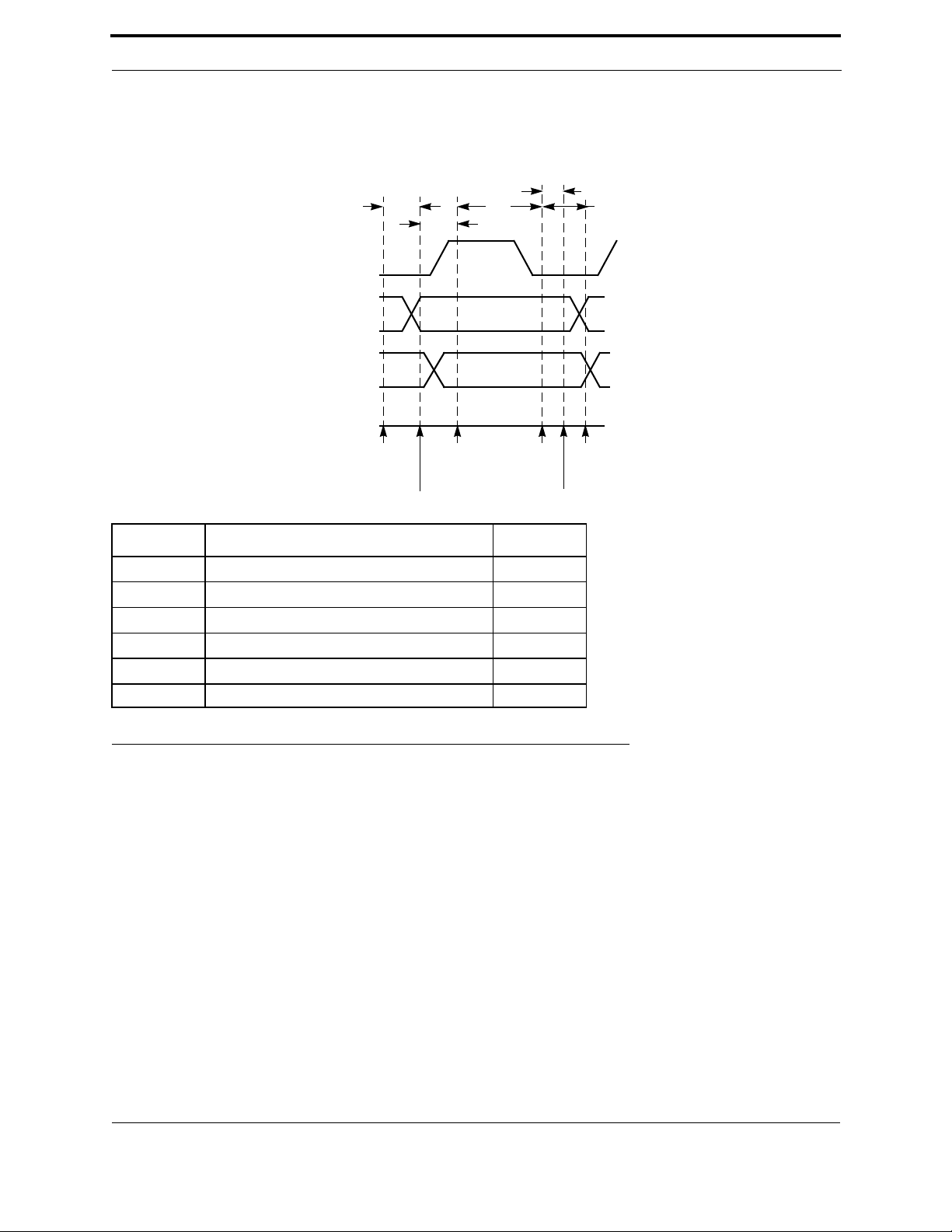
Serial I/O Objects
t
the active edge of the clock to negative. One of the IO0 – IO7 pins may be designated as a timeout pin. A logic 1
level on the timeout pin causes the Neurowire slave I/O operation to be terminated before the specified number of bits
has been transferred. This prevents the FT Smart Transceiver watchdog timer from resetting the chip in the event that
fewer than the requested number of bits are transferred by the external clock. See Figure 3.30.
DATA
t
docki
t
cklo
CLOCK
SAMPLED
t
fin
INPUT
CLOCK
DATA OUT
DATA IN
TIME
START
OF
io_in()
DATA
OUTPUT
CLOCK AND
SAMPLED
Parameter Description Typ
t
fin
t
ret
t
docki
t
cklo
t
cklodo
Function call to data bit out 41.4 µs
Return from function 19.2 µs
Data out to input clock and data sampled 4.8 µs
Data sampled to clock low sampled 24.0 µs
Clock low sampled to data output 25.8 µs
f Clock frequency (max) 18.31 kHz
OUTPUT
END OF
io_in()
ret
DATA
t
cklodo
Figure 3.30 Neurowire (SPI) Slave Timing
The algorithm for each bit of output/input for the Neurowire slave objects is described below. In this description, the
default active clock edge (positive) is assumed; if the invert keyword is used, all clock levels stated should be
reversed.
1. Set IO9 to the next output bit value.
2. Test pin IO8, the clock input, for a high level. This is the test for the rising edge of the input clock. If the input
clock is still low, sample the timeout event pin and abort if high.
3. When the input clock is high, store the next data input bit as sampled on pin IO10.
4. Test the input clock for a low input level. This is the test for the falling edge of the input clock. If the input clock
is still high, sample the timeout event pin and abort if high.
5. When the input clock is low, return to step 1 if there are more bits to be processed.
6. Else return the number of bits processed.
When either clock input test fails (that is, the clock is sampled before the next transition), there is an additional
timeout check time of 19.8 µs (wait for clock high) or 19.2 µs (wait for clock low) added to that stage of the
algorithm.
FT 3120 / FT 3150 Smart Transceiver Data Book 65
Page 72
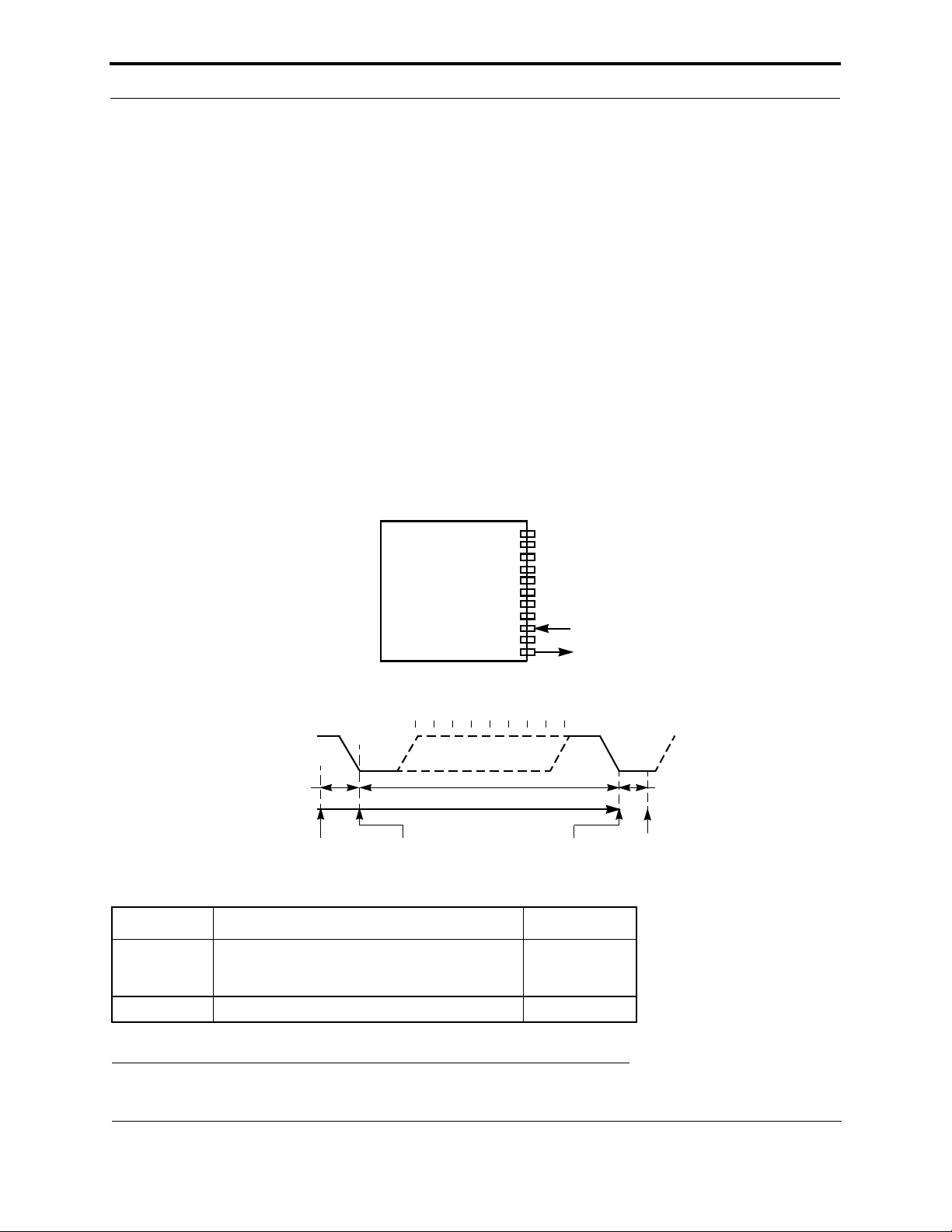
Chapter 3 - Input/Output Interfaces
The chip select logic for the Neurowire slave can be handled by the user through a separate bit input object, along
with an appropriate handshaking algorithm implemented by the user application program. In order to prevent
unnecessary timeouts, the setup and hold times of the chip select line, relative to the start and end of the external
clock, must be satisfied.
The timeout input pin can either be connected to an external timer or to an output pin of the FT Smart Transceiver that
is declared as a oneshot object.
Serial Input/Output
Pin IO8 may be configured as an asynchronous serial input line, and pin IO10 may be configured as an asynchronous
serial output line. The bit rates for input and for output may be independently specified to be 600, 1200, 2400, or
4800 bits/second at a 10MHz input clock rate. The data rate scales proportionally to the input clock rate. For example,
at 40MHz, the bit rates would be 2400, 4800, 9600, or 19,200 bits/second.
The frame format is fixed at 1 start bit, 8 data bits, and 1 stop bit; and up to 255 bytes may be transferred at a time.
Either a serial input or a serial output operation (but not both) may be in effect at any one time. The interface is halfduplex only. This function suspends application processing until the operation is completed. On input, the io_in()
request will time out after 20 character times if no start bit is received. If the stop bit has the wrong polarity (it
should be a 1), the input operation is terminated with an error. The application code can use bit I/O pins for
flow control handshaking if required. This function is useful for transferring data to serial devices such as
terminals, modems, and computer serial interfaces. See Figures 3.31 and 3.32.
IO0
IO1
IO2
IO3
IO4
IO5
IO6
SERIAL
INPUT
t
TIME
START OF
fin
io_in()
START
START BIT
APPEARS
IO7
IO8
IO9
IO10
DATA
ONE FRAME
Serial Input
Serial Output
87654321
END OF
FRAME
STOP
Symbol Description Typ @ 10MHz
t
fin
t
ret
Function call to input sample
Min (first sample)
Max (timeout)
67 µs
20 byte frame
Return from function 10 µs
START
t
END OF
io_in()
ret
Figure 3.31 Serial Input Object
66 FT 3120 / FT 3150 Smart Transceiver Data Book
Page 73
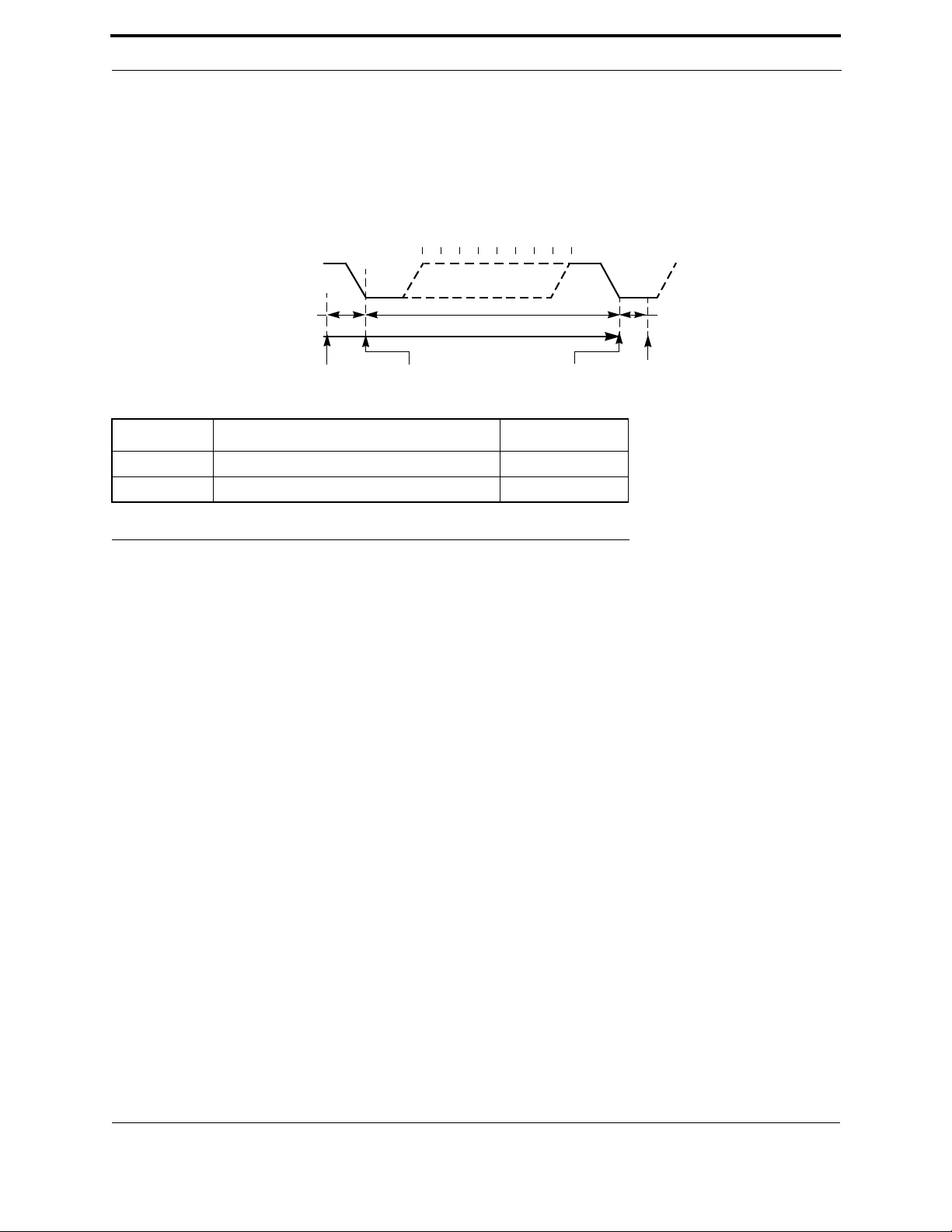
Serial I/O Objects
The duration of this function call is a function of the number of data bits transferred and the transmission bit rate. t
fin
(max) refers to the maximum amount of time this function will wait for a start bit to appear at the input. After
this time, the function will return a 0 as data. t
example, the timeout period at 2400 bits/second is (20 x 10 x 1/2400) + t
SERIAL
OUTPUT
t
fout
TIME
START OF
io_out()
Symbol Description Typ @ 10MHz
t
t
fout
ret
Function call to start bit 79 µs
Return from function 10 µs
(min) is the time to the first sampling of the input pin. As an
fin
(min).
fin
DATA
87654321
START
START BIT
APPEARS
STOP
ONE FRAME
END OF
FRAME
START
t
END OF
io_in()
ret
Figure 3.32 Serial Output
The duration of this function call is a function of the number of data bits transferred and the transmission bit rate. As
an example, to output 100 bytes at 300 bits/second would require a time duration of (100 x 10 x 1/300) + t
fout
+ t
ret
Touch Input/Output
The Touch I/O object enables easy interface to any slave device which adheres to the Dallas Semiconductor Touch
Memory™ standard. This interface is a one-wire, open-drain, bidirectional connection.
Up to eight Touch Memory busses may be connected to a FT Smart Transceiver through the use of the first eight I/O
pins, IO0 – IO7. The only additional component required for this is a pull-up resistor on the data line (refer to the
Touch Memory specification below on how to select the value of the pull-up resistor). The high current sink
capabilities of IO0 – IO3 pins of the FT Smart Transceiver can be used in applications where long wire lengths are
required between the Touch Memory device and the FT Smart Transceiver.
The slave acquires all necessary power for its operation from the data line. Upon physical connection of a Touch
Memory device to a master (in this case the FT Smart Transceiver), the Touch Memory generates a low presence
pulse to inform the master that it is awaiting a command. The FT Smart Transceiver can also request a presence pulse
by sending a reset pulse to the Touch Memory device.
Commands and data are sent bit by bit to make bytes, starting with the LSB. The synchronization between the FT
Smart Transceiver and the Touch Memory devices is accomplished through a negative-going pulse generated by the
FT Smart Transceiver.
Figure 3.33 shows the details of the reset pulse in addition to the read/write bit slots.
.
FT 3120 / FT 3150 Smart Transceiver Data Book 67
Page 74

Chapter 3 - Input/Output Interfaces
RESET
AND
PRESENCE
DATA LINE
TIME
START OF
touch_reset()
IO0
IO1
IO2
IO3
IO4
IO5
IO6
IO7
IO8
IO9
IO10
High Current Sink Drivers
t
rsto
t
rstl
SAMPLED
INPUT
t
pd
t
wh
LINE TYPE LEGEND
t
pdl
t
END OF
touch_reset()
FT Smart Transceiver
TOUCH MEMORY
PULL-UP RESISTOR
WRITE 1
WRITE 0
rret
READ
DATA LINE
DATA LINE
DATA LINE
START OF io_in() OR
TIME
io_out()
t
f
t
t
rdi
INPUT
SAMPLED
wrd
t
low
t
ibd
t
ret
io_in() OR
Symbol Description Min Ty p Max
t
t
t
t
t
t
t
t
t
t
t
t
rsto
rstl
pdh
pdl
wh
rret
f
low
rdi
wrd
ibd
ret
Reset call to data line low — 60.0 µs —
Reset pulse width — 500 µs —
Reset pulse release to data line high
10MHz
5MHz
4.8 µs
9.6 µs
—
—
275 µs
275 µs
Presence pulse width — 120.0 µs —
Data line high detect to presence pulse — 80 µs —
Return from reset function — 12.6 µs —
I/O call to data line low (start of bit slot) — 125.4 µs —
Start pulse width
10MHz
5MHz
—
—
4.2 µs
8.4 µs
—
—
Start pulse edge to sampling of input (read operation)
10MHz
5MHz
—
—
15.0 µs
18.0 µs
—
—
Start pulse edge to FT Smart Transceiver releasing the data line
10MHz
5MHz
—
—
66.6 µs
72.0 µs
—
—
Inter-bit delay
10MHz
5MHz
—
—
61.2 µs
122.4 µs——
Return from I/O call — 42.6 µs —
END OF
io_out()
NEXT
io_in() OR
io_out()
Figure 3.33 Touch I/O Object
The leveldetect input object can be used for detection of asynchronous attachments of Touch Memory devices to the
FT Smart Transceiver. In such a case, the leveldetect input object is overlaid on top of the Touch I/O object. Refer to
the Neuron C Programmer’s Guide for information on I/O object overlays.
68 FT 3120 / FT 3150 Smart Transceiver Data Book
Page 75

Serial I/O Objects
The Touch I/O object can run at FT Smart Transceiver clock rates of 5MHz and 10MHz only. This is because the
Touch I/O object is designed to meet the Touch Memory timing specification at those FT Smart Transceiver clock
speeds only. The Touch I/O object is not supported at clock rates faster than 10MHz or slower than 5MHz.
For more specific information on the mechanical, electrical, and protocol specifications, refer to the Book of DS19xx
Touch Memory Standards, available from Dallas Semiconductor Corporation.
Wiegand Input
This input object provides an easy interface to any card reader supporting the Wiegand standard. Data from the reader
is presented to the FT Smart Transceiver through the use of two of its first eight I/O pins, IO0 – IO7. Up to four
Wiegand devices may be connected to the FT Smart Transceiver. Data is read MSB first.
Wiegand data starts as a negative-going pulse on one of the two pins selected. One input represents a logical 0 bit and
the other pin a logical 1, as selected through the I/O declaration. The bit data on the two lines are mutually exclusive
and are spaced at least 150 µs apart. Figure 3.34 shows the timing relationship of the two data lines with respect
to each other and the FT Smart Transceiver.
Any unused I/O pin from IO0 to IO7 may be optionally selected as the timeout pin. When the timeout pin goes high,
the function aborts and returns. The watchdog timer of the application processor is automatically updated during the
operation of this input object.
Incoming data on any of the Wiegand input pins is sampled by the FT Smart Transceiver every 200ns at a 10MHz
clock (scales inversely with the clock frequency). Since the Wiegand data is usually asynchronous, care must be
taken in the application program to ensure that this function is called in a timely manner in order that no incoming
data is lost.
FT 3120 / FT 3150 Smart Transceiver Data Book 69
Page 76

Chapter 3 - Input/Output Interfaces
DATA A
DATA B
TIMEOUT
TIME
IO0
IO1
IO2
IO3
IO4
IO5
IO6
IO7
IO8
IO9
IO10
Optional Pull-Up Resistors
t
dw
t
ibd
t
fin
t
tret
t
ret
t
tow
START OF
io_in()
END OF
io_in()
Symbol Description Min Ty p Max
t
t
t
t
t
t
fin
dw
ibd
tow
tret
ret
Function call to start of second data edge — 75.6 µs —
Input data width (at 10MHz) 200 ns 100 µs 880 ms
Inter-bit delay 150 µs — 900 µs
Timeout pulse width — 39 µs —
Timeout to function return — 18.0 µs —
Last data bit to function return — 74.4 µs —
Figure 3.34 Wiegand Input Object
Timer/Counter Input Objects
The FT Smart Transceivers have two 16-bit timer/counters. For the first timer/counter, IO0 is used as the output, and
a multiplexer selects one of IO4 – IO7 as the input. The second timer/counter uses IO1 as the output and IO4 as the
input (see Figure 2.7). Multiple timer/counter input objects may be declared on different pins within a single
application. By calling the io_select() function, the application can use the first timer/counter in up to four
different input functions. If a timer/counter is configured in one of the output functions, or as a quadrature
input, then it can not be reassigned to another timer/counter object in the same application program.
The timing numbers shown in this section are valid for both an explicit I/O call or an implicit I/O call through a when
clause, and are assumed to be for a FT Smart Transceiver running at 10MHz.
70 FT 3120 / FT 3150 Smart Transceiver Data Book
Page 77

Timer/Counter Input Objects
Input timer/counter objects have the advantage (over non-timer/counter objects) in that input events will be captured
even if the application processor is occupied doing something else when the event occurs. A true when statement
condition for an event being measured by a timer/counter is the completion of the measurement and a value
being returned to an event register. If the processor is delayed due to software processing and cannot read the
register before another event occurs, then the value in the register will reflect the status of the last event. The
timer/counters are automatically reset upon completion of a measurement. The first measured value of a
timer/counter is always discarded to eliminate the possibility of a bad measurement after the chip comes
out of a reset condition. Single events can not be measured with the timer/counters. Figure 3.35 shows an
example of how the timer/counter objects are processed with a Neuron C when statement.
Example of a
when statement
evaluating true
(unless it is the
first event)
Example of a
when statement
missing a present
event but evaluating a previous
event
READ TIMER/COUNTER FLAG AND REGISTER
INPUT
SIGNAL
(event)
TIME
INPUT
SIGNAL
TIME
START
TIMER/
COUNTER
t
fin
START
TIMER/
COUNTER
FROM THE PREVIOUS EVENT
START OF
io_in()
STOP
TIMER/COUNTER
SET FLAG
LOAD EVENT
REGISTER
t
ret
END OF
io_in()
STOP TIMER/COUNTER
SET FLAG LOAD NEW VALUE
INTO REGISTER
START OF
io_in()
(when
statement)
t
fin
READ
TIMER/
COUNTER
FLAG AND
REGISTER
CLEAR FLAG
t
ret
END OF
io_in()
Figure 3.35 Example of when Statement Processing Using the Ontime Input Function
Dualslope Input
This input object uses a timer/counter to control and measure the integration periods of a dualslope integrating analog
to digital converter (see Figure 3.36). The timer/counter provides the control output signal and senses a comparator
output signal. The control output signal controls an external analog multiplexer which switches between the unknown
input voltage and a voltage reference. The input pin of the timer/counter is driven by an external comparator which
compares the output of the integrator with a voltage reference. At the end of conversion, the external comparator will
drive a low level to one of pins IO4 – IO7. If external circuitry indicates “end of conversion” with a high level, use
the invert keyword in the I/O declaration.
FT 3120 / FT 3150 Smart Transceiver Data Book 71
Page 78

Chapter 3 - Input/Output Interfaces
The resolution and range of the timer/counter period options is shown by Table 3.6 in section , Notes, at the end of
this chapter.
OUTPUT
(IO0 OR IO1)
INPUT
(IO4 TO IO7)
TIME
Timer/Counter 1
Timer/Counter 2
t
reqo
mux
IO0
Control Output
IO1
IO2
IO3
IO4
IO5
IO6
IO7
IO8
IO9
IO10
t
fin
From
Comparator
ANALOG SWITCH
CONTROL
COMPARATOR
OUTPUT
INTEGRATOR
OUTPUT
V
thresh
START OF
io_in_request()
LATCHED COUNT
AVAI L AB L E TO
APPLICATION
START
OF io_in()
END OF
io_in()
Symbol Description Min Typ Max
t
reqo
t
fin
io_in_request() to output toggle — 75.6 µs —
Input function call and return — 82.8 µs —
Figure 3.36 Dualslope Input Object
Edgelog Input
The edgelog input object can record a stream of input pulses measuring the consecutive low and high periods at the
input and storing them in user-defined storage (see Figure 3.37). The values stored represent the units of clock period
between rising and falling input signal edges. Both timer/counters of the FT Smart Transceiver are used for this
object.
The measurement series starts on the first rising (positive) edge, unless the invert keyword is used in the I/O object
declaration. The measurement process stops whenever an overflow condition is sensed on either timer/counter.
72 FT 3120 / FT 3150 Smart Transceiver Data Book
Page 79

Timer/Counter Input Objects
The resolution and range of the timer/counter period options are shown in Table 3.6 in section , Notes. This object is
useful for analyzing an arbitrarily-spaced stream of input edges (or pulses), such as the output of a UPC bar-code
reader or infrared receiver.
IO0
IO1
IO2
IO3
IO4
IO5
IO6
IO7
IO8
IO9
IO10
Input
Bit Stream
INPUT
(IO4)
Timer/Counter 1
Timer/Counter 2
t
t
wtcp
win
t
ret
TIME
START OF
io_in()
t
setup
t
hold
OVERFLOW
Symbol Description Min Typ Max
t
setup
t
win
t
hold
Input data setup 0 — —
Input pulse width 1 T/C clk — 65,534 T/C clks
io_in() call to data input edge for
26.4 µs — —
inclusion of that pulse
t
wtcp
t
oret
t
ret
Two consecutive pulse widths 104 µs — —
Return on overflow — 42.6 µs —
Return on count termination — 49.6 µs —
Note: T/C clk represents the period of the clock used during the declaration of the I/O object.
Figure 3.37 Edgelog Input Object
Infrared Input
END
OF io_in()
t
oret
The infrared input object is used to capture a stream of data generated by a class of infrared remote control devices
(see Figure 3.38). The input to the object is the demodulated series of bits from infrared receiver circuitry. The period
of the on/off cycle determines the data bit value, a shorter cycle indicating a one, and a longer cycle indicating a zero.
The actual threshold for the on/off determination is set at the time of the call of the function. The measurements are
made between the negative edges of the input bits unless the invert keyword is used in the I/O declaration.
FT 3120 / FT 3150 Smart Transceiver Data Book 73
Page 80

Chapter 3 - Input/Output Interfaces
The infrared input object, based on the input data stream, generates a buffer containing the values of the bits received.
The resolution and range of the timer/counter period options is shown in Table 3.6 in section , Notes, at the end of this
chapter.
This function can be used with an off-the-shelf IR demodulator such as an NEC µPD1913 or Sharp GP1U50X to
quickly develop an infrared interface to the FT Smart Transceiver. The edgelog input object can also be used
for this purpose. However, this requires more code.
Timer/Counter 1
Timer/Counter 2
INPUT
(IO0 TO IO7)
TIME
START OF
io_in()
mux
t
win (1 BIT)
t
fin
IO0
IO1
IO2
IO3
IO4
IO5
IO6
IO7
IO8
IO9
IO10
t
ret
END OF
io_in()
Input
Data Stream
Symbol Description Min Typ Max
t
t
t
fin
ret
win
Function call to start of input sampling — 82.2 µs —
End of last valid bit to function return max-
period
maxperiod
—
Minimum input period width — 93 µs —
Note: max-period is the timeout period passed to the function at the time of the call.
Figure 3.38 Infrared Input Object
Ontime Input
A timer/counter may be configured to measure the time for which its input is asserted. Table 3.6 shows the resolution
and maximum times for different I/O clock selections. Assertion may be defined as either logic high or logic low.
This object may be used as a simple analog-to-digital converter with a voltage-to-time circuit, or for measuring
velocity by timing motion past a position sensor. See Figures 3.35 and 3.39.
74 FT 3120 / FT 3150 Smart Transceiver Data Book
Page 81

Timer/Counter Input Objects
IO0
IO1
IO2
IO3
IO4
IO5
IO6
IO7
IO8
IO9
IO10
Reference Figure 3.35
mux
System Clock
Divide Chain
Optional Pull-Up Resistors
Event Register
Timer/Counter 2
Timer/Counter 1
Event Register
Symbol Description Typ @ 10MHz
t
fin
t
ret
*If the measurement is new, t
Function call to input sample 86 µs
Return from function 52/22 µs*
= 52 µs. If a new time is not being returned, t
ret
ret
= 22 µs.
Figure 3.39 Ontime Latency Values
This is a level-sensitive function. The active level of the input signal gates the clock driving the internal counter in the
FT Smart Transceiver.
The actual active level of the input depends on whether or not the invert option was used in the declaration of the
function block. The default is the high level.
Period Input
A timer/counter may be configured to measure the period from one rising or falling edge to the next corresponding
edge on the input. Table 3.6 shows the resolution and maximum time measured for various clock selections. This
object is useful for instantaneous frequency or tachometer applications. Analog-to-digital conversion can be
implemented using a voltage-to-frequency converter with this object. See Figure 3.40.
FT 3120 / FT 3150 Smart Transceiver Data Book 75
Page 82
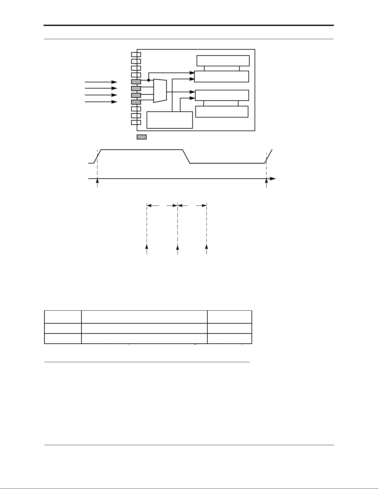
Chapter 3 - Input/Output Interfaces
INPUT
TIME
START
TIMER
IO0
IO1
IO2
IO3
IO4
IO5
IO6
IO7
IO8
IO9
IO10
mux
System Clock
Divide Chain
Optional Pull-Up Resistors
t
fin
t
ret
Event Register
Timer/Counter 2
Timer/Counter 1
Event Register
STOP TIMER
COUNTER
START OF
io_in()
READ
TIMER/COUNTER
FLAG AND
EVENT
REGISTER
CLEAR FLAG
END OF
io_in()
Reference Figure 3.35
Symbol Description Typ @ 10MHz
t
fin
t
ret
*If the measurement is new, t
Function call to input sample 86 µs
Return from function 52/22 µs*
= 52 µs. If a new time is not being returned, t
ret
ret
= 22 µs.
Figure 3.40 Period Input Latency Values
This is an edge-sensitive function. The clock driving the internal counter in the FT Smart Transceiver is free running.
The detection of active input edges stops and resets the counter each time.
The actual active edge of the input depends on whether or not the invert option was used in the declaration of the
function block. The default is the negative edge.
Since the period function measures the delay between two consecutive active edges, the invert option has no effect on
the returned value of the function for a repeating input waveform.
76 FT 3120 / FT 3150 Smart Transceiver Data Book
Page 83

Timer/Counter Input Objects
Pulsecount Input
A timer/counter may be configured to count the number of input edges (up to 65,535) in a fixed time (0.8388608
second) at all allowed input clock rates. Edges may be defined as rising or falling. This object is useful for average
frequency measurements, or tachometer applications. See Figure 3.41.
TART O F
o_in()
READ
t
ret
t
fin
TIMER/COUNTER
FLAG AND
EVENT
REGISTER
CLEAR FLAG
IO0
IO1
IO2
IO3
IO4
IO5
IO6
IO7
IO8
IO9
IO10
END OF
io_in()
mux
System Clock
Divide Chain
Optional Pull-Up Resistors
Event Register
Timer/Counter 2
Timer/Counter 1
Event Register
0.84 s
STOPSTART
Reference Figure 3.35
Symbol Description Typ @ 10MHz
t
fin
t
ret
*If the measurement is new, t
Function call to input sample 86 µs
Return from function 52/22 µs*
= 52 µs. If a new time is not being returned, t
ret
= 22 µs.
ret
Figure 3.41 Pulse Count Input Latency Values
This is an edge-sensitive function. The clock driving the internal counter in the FT Smart Transceiver is the actual
input signal. The counter is reset automatically every 0.839 second.
The internal counter increments with every occurrence of an active input edge. Every 0.839 second, the content of the
counter is saved and the counter is then reset to 0. This sequence is repeated indefinitely.
The actual active edge of the input depends on whether or not the invert option was used in the declaration of the
function block. The default is the negative edge.
FT 3120 / FT 3150 Smart Transceiver Data Book 77
Page 84
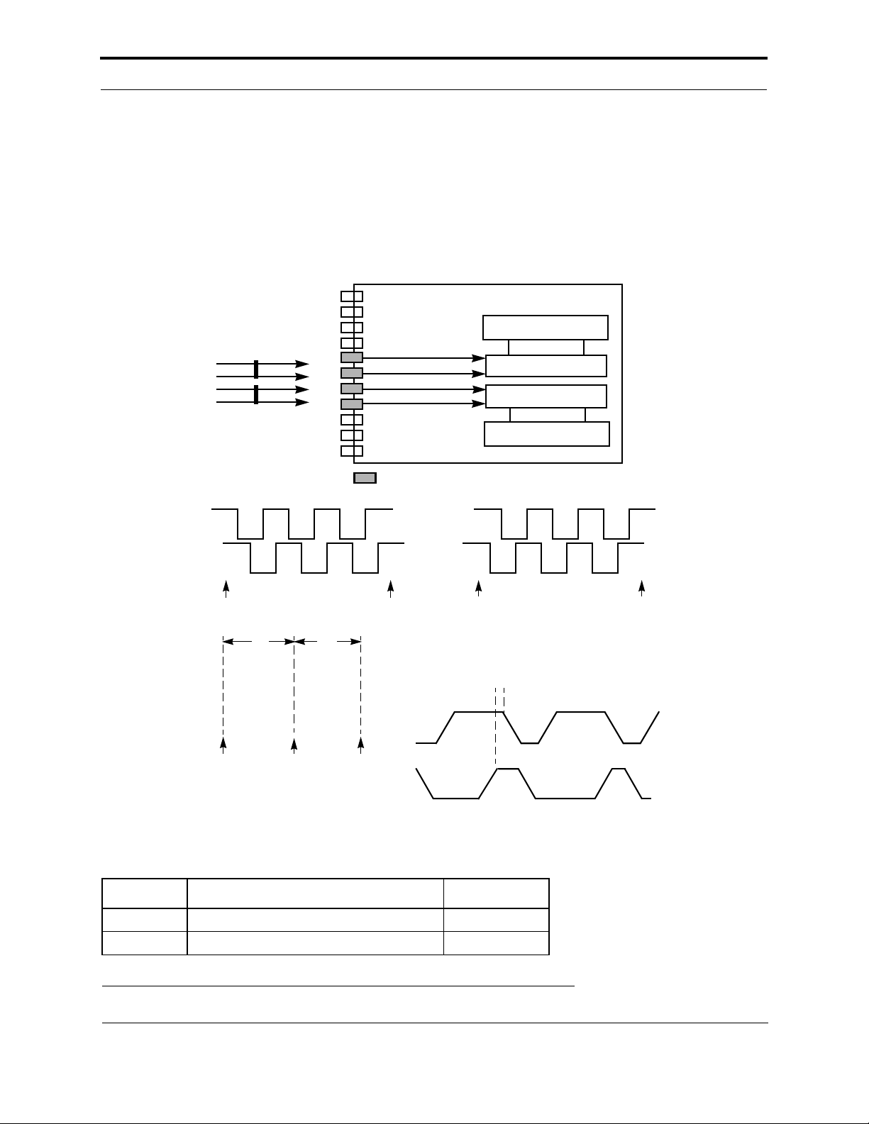
Chapter 3 - Input/Output Interfaces
Quadrature Input
A timer/counter may be configured to count transitions of a binary Gray code input on two adjacent input pins. The
Gray code is generated by devices such as shaft encoders and optical position sensors which generate the bit pattern
(00,01,11,10,00, …) for one direction of motion and the bit pattern (00,10,11,01,00, …) for the opposite direction.
Reading the value of a quadrature object gives the arithmetic net sum of the number of transitions since the last time
it was read (– 16,384 to 16,383). The maximum frequency of the input is one-quarter of the input clock rate, for
example 2.5MHz at 10MHz FT Smart Transceiver input clock. Quadrature devices may be connected to timer/
counter 1 via pins IO6 and IO7, and timer/counter 2 via pins IO4 and IO5. If the second input transitions low while
the first input is low and high while the first input is high, the counter counts up. Otherwise, the count is down.
IO0
IO1
IO2
IO3
IO4
IO5
IO6
IO7
IO8
IO9
IO10
Optional Pull-Up Resistors
Event Register
Timer/Counter 2
Timer/Counter 1
Event Register
INPUT 1
INPUT 2
Count + 6 counts Count – 6 counts
START OF
io_in()
t
fin
TIMER/COUNTER
FLAG AND
EVENT
REGISTER
CLEAR FLAG
READ
t
ret
END OF
io_in()
A
B
2 x CLK1 Period, Ex: 200 ns @ 10MHz
(minimum time allowed
between consecutive transitions)
Reference Figure 3.35
Symbol Description Typ @ 10MHz
t
fin
t
ret
Function call to input sample 90 µs
Return from function 88 µs
read, resetread, resetread, resetread, reset
Figure 3.42 Quadrature Input Latency Values
78 FT 3120 / FT 3150 Smart Transceiver Data Book
Page 85
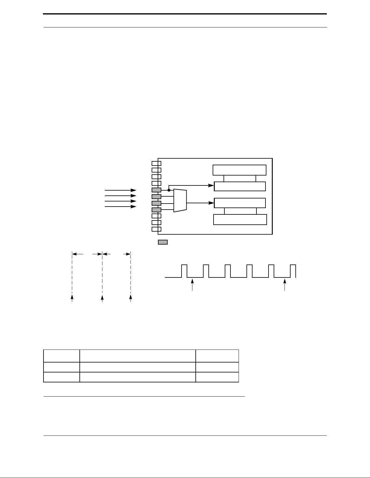
Timer/Counter Input Objects
A call to this function returns the current value of the quadrature count since the last read operation. The counter is
then reset and ready for the next series of input transitions. The count returned is a 16-bit signed binary number,
capped at ±16K.
The number shown in the diagram above is the minimum time allowed between consecutive transitions at either input
of the quadrature function block. For more information, see the, Neuron Chip Quadrature Input Function Interface
engineering bulletin.
Totalcount Input
A timer/counter may be configured to count either rising or falling input edges, but not both. Reading the value of a
totalcount object gives the number of transitions since the last time it was read (0 to 65,535). Maximum frequency of
the input is one-quarter of the input clock rate, for example 2.5MHz at a maximum of 10MHz FT Smart Transceiver
input clock. This object is useful for counting external events such as contact closures, where it is important to keep
an accurate running total. See Figure 3.43.
IO0
IO1
IO2
IO3
IO4
IO5
IO6
IO7
IO8
IO9
IO10
mux
Event Register
Timer/Counter 2
Timer/Counter 1
Event Register
Optional Pull-Up Resistors
START OF
io_in()
t
fin
TIMER/
COUNTER
FLAG AND
EVENT REGISTER
CLEAR FLAG
READ
t
ret
END OF
io_in()
Reference Figure 3.35
Symbol Description Typ @ 10MHz
t
fin
t
ret
Function call to input sample 92 µs
Return from function 61 µs
Figure 3.43 Totalcount Input Latency Values
read input_value = 4, resetread, reset
FT 3120 / FT 3150 Smart Transceiver Data Book 79
Page 86

Chapter 3 - Input/Output Interfaces
A call to this function returns the current value of the totalcount value corresponding to the total number of active
clock edges since the last call. The counter is then reset, and ready for the next series of input transitions.
The actual active edge of the input depends on whether or not the invert option was used in the declaration of the
function block. The default is the negative edge.
Timer/Counter Output Objects
Edgedivide Output
This output object acts as a frequency divider by providing an output frequency on either pin IO0 or IO1. The output
frequency is a divided-down version of the input frequency applied on pins IO4 – IO7. The object is useful for any
divide-by-n operation, where n is passed to the timer/counter object through the application program and can be from
1 to 65,535. The value of 0 forces the output to the off level and halts the timer/counter.
A new divide value will not take effect until after the output toggles, with two exceptions: if the output is initially
disabled, the new (non-zero) output will start immediately after t
disabled immediately.
Normally the negative edges of the input sync pulses are the active edge. Using the invert keyword in the object
declaration makes the positive edge active.
The initial state of the output pin is logic 0 by default. This can also be changed to logic 1 through the object
declaration.
; or, for a new divide value of 0, the output is
fout
Figure 3.44 shows the pinout and timing information for this output object.
80 FT 3120 / FT 3150 Smart Transceiver Data Book
Page 87
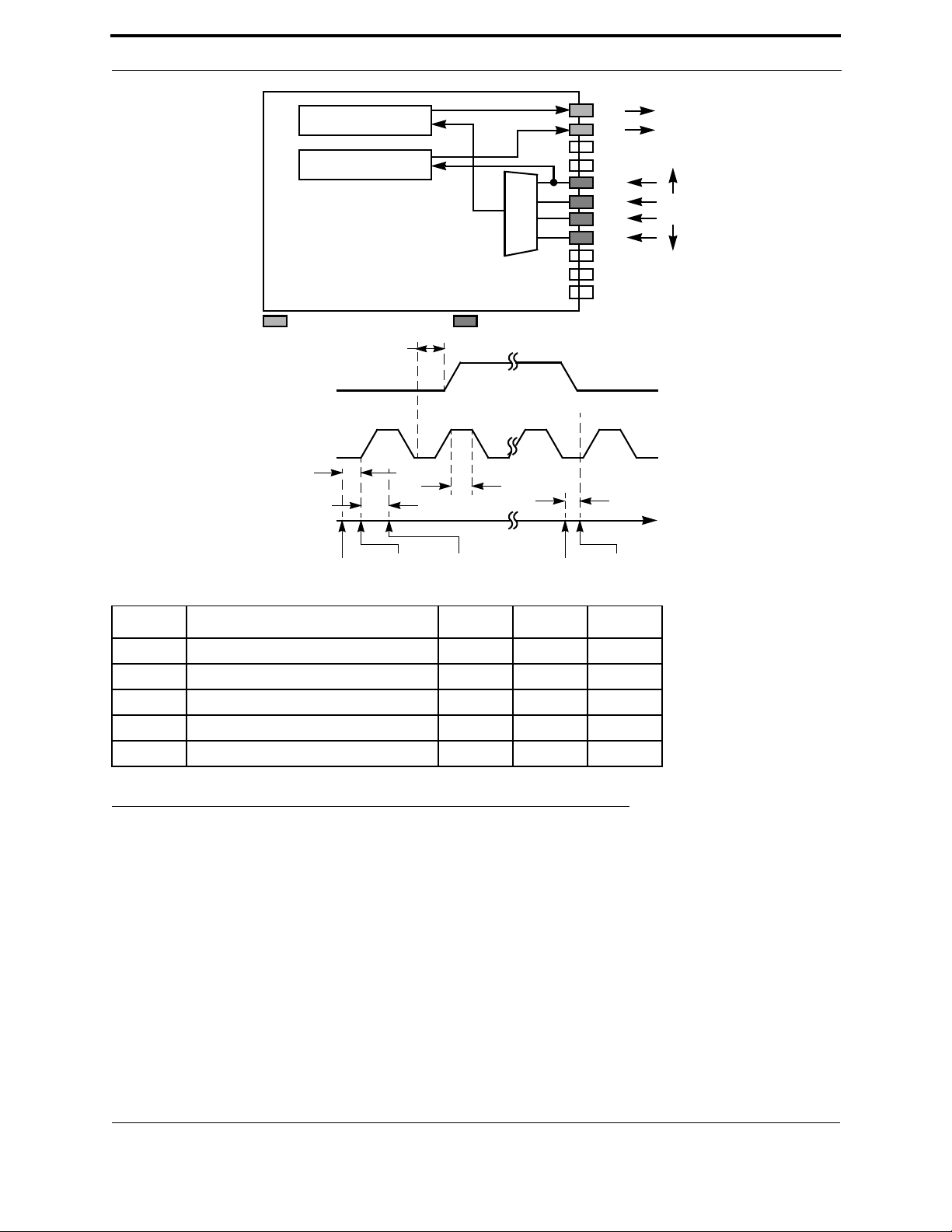
Timer/Counter Output Objects
OUTPUT
SYNC INPUT
TIME
START OF
io_out()
Timer/Counter 1
Timer/Counter 2
t
INTERNAL
COUNT
BEGINS
sod
t
fout
IO0
IO1
Output
IO2
IO3
IO4
mux
IO5
IO6
Sync
Input
IO7
IO8
IO9
IO10
Optional Pull-Up ResistorsHigh Current Sink Drivers
t
win
t
t
ret
END OF
io_out()
fod
START OF
io_out()
OUTPUT
INACTIVE
Symbol Description Min Typ Max
t
fout
t
fod
t
sod
t
win
t
ret
Function call to start of timer — 96 µs —
Function to output disable — 82.2 µs —
Active sync edge to output toggle 550 ns — 750 ns
Sync input pulse width (10MHz) 200 ns — —
Return from function — 13 µs —
Figure 3.44 Edgedivide Output Object
Frequency Output
A timer/counter may be configured to generate a continuous square wave of 50% duty cycle. Writing a new
frequency value to the device takes effect at the end of the current cycle. This object is useful for frequency synthesis
FT 3120 / FT 3150 Smart Transceiver Data Book 81
Page 88
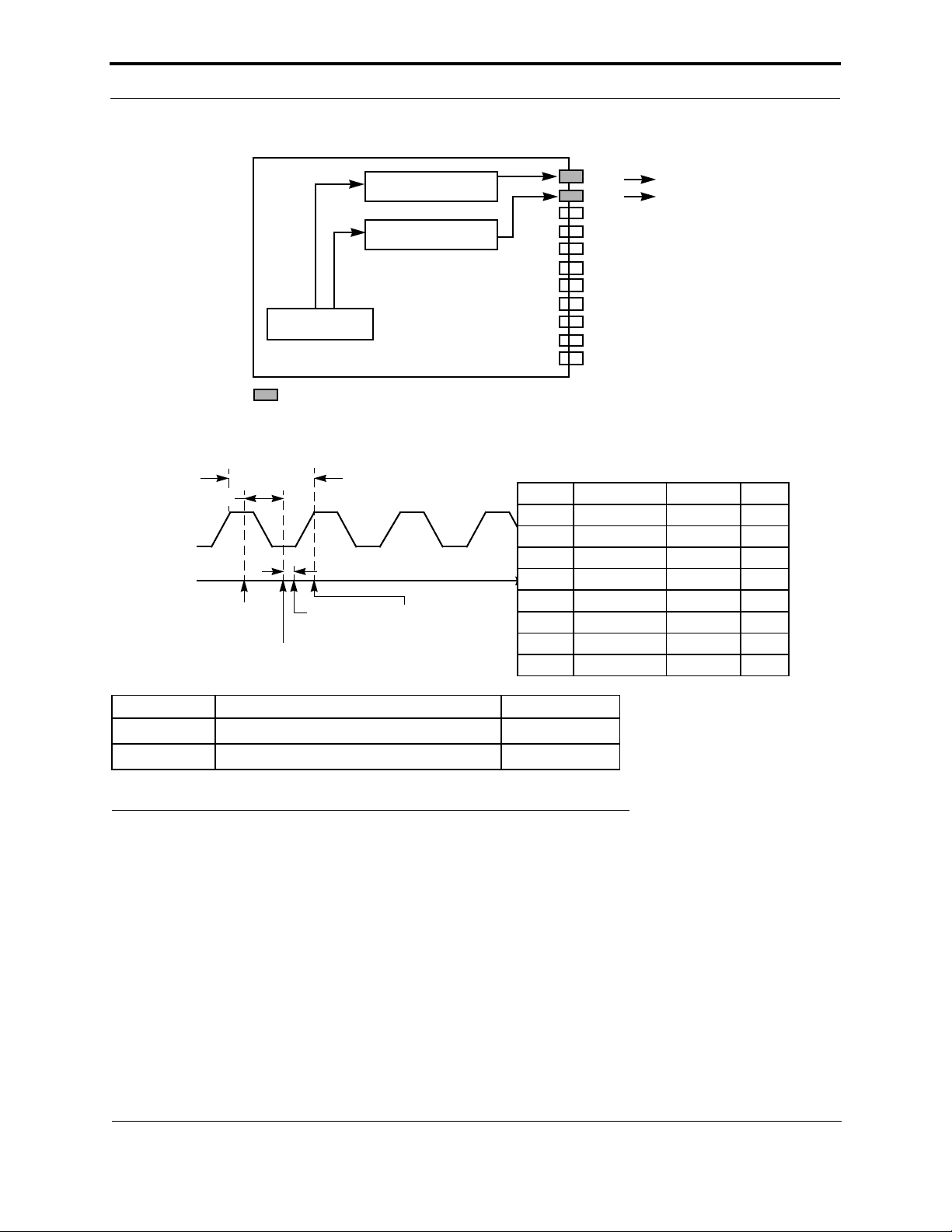
Chapter 3 - Input/Output Interfaces
to drive an audio transducer, or to drive a frequency to voltage converter to generate an analog output. See
Figure 3.45.
FREQUENCY
OUTPUT
TIME
ONE CYCLE
t
fout
t
ret
START
OF io_out()
INTERNALLY
System Clock
Divide Chain
High Current Sink Drivers
END
OF io_out()
HARDWARE
UPDATED
Timer/Counter 1
Timer/Counter 2
Frequency Resolution and
Maximum Range at 10MHz
CLK Resolution Range Unit
0 0.4 26.21 µs
1 0.8 52.42 µs
2 1.6 104.86 µs
3 3.2 209.71 µs
NEW OUTPUT
APPEARS ON PIN
4 6.4 419.42 µs
5 12.8 838.85 µs
6 25.6 1677 µs
7 51.2 3355 µs
IO0
IO1
IO2
IO3
IO4
IO5
IO6
IO7
IO8
IO9
IO10
Symbol Description Typ @ 10MHz
t
t
fout
ret
Function call to output update 96 µs
Return from function 13 µs
Figure 3.45 Frequency Output Latency Values
A new frequency output value will not take effect until the end of the current cycle. There are two exceptions to this
rule. If the output is disabled, the new (non-zero) output will start immediately after
t
. Also, for a new output value
fout
of zero, the output is disabled immediately and not at the end of the current cycle.
A disabled output is a logic zero by default unless the invert keyword is used in the I/O object declaration. The
resolution and range for this object scale with FT Smart Transceiver input clock rate, for example: resolution
from 0.1 to 12.8 µs and range from 6.55 to 839 ms at 40MHz.
82 FT 3120 / FT 3150 Smart Transceiver Data Book
Page 89
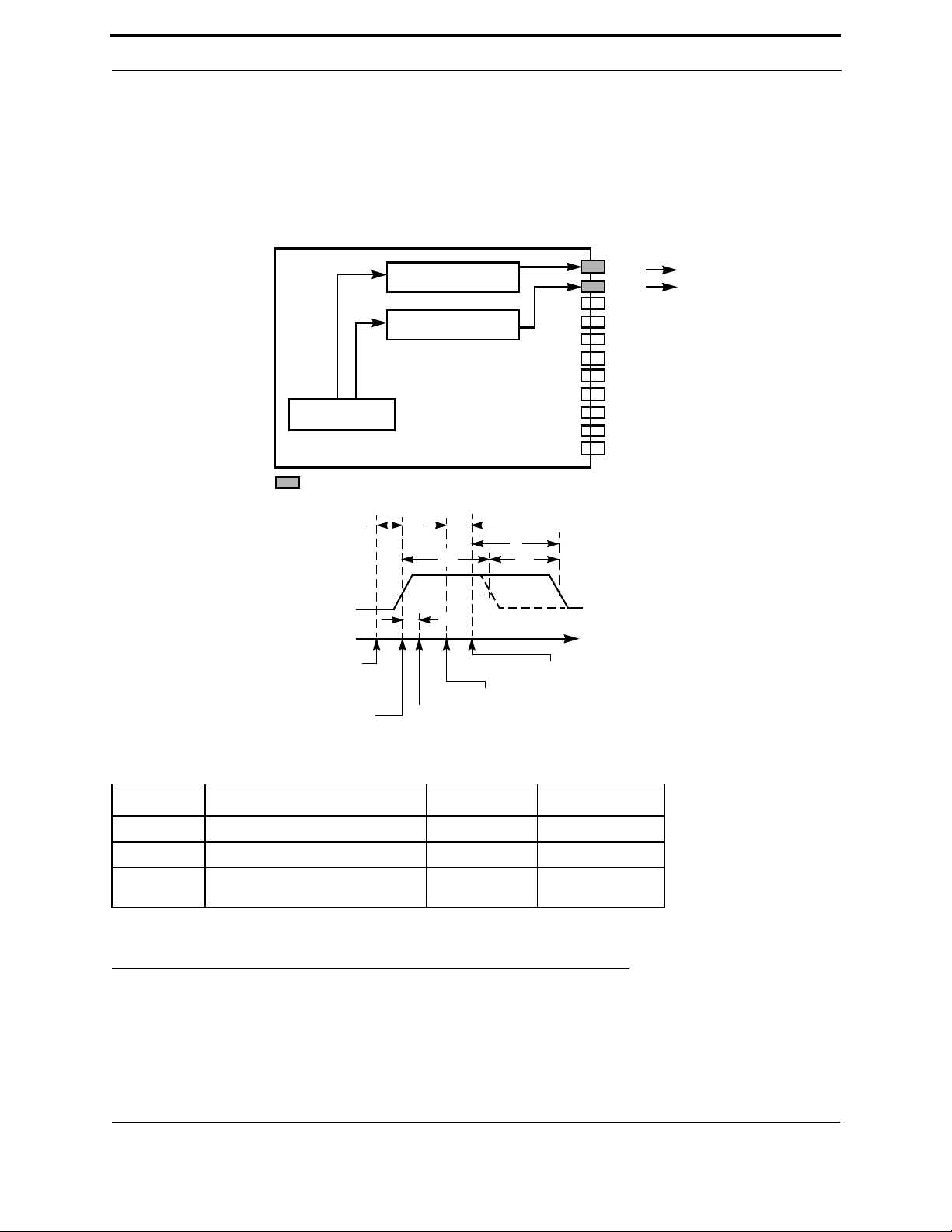
Timer/Counter Output Objects
Oneshot Output
A timer/counter may be configured to generate a single pulse of programmable duration. The asserted state may be
either logic high or logic low. Retriggering the oneshot before the end of the pulse causes it to continue for the new
duration. Table 3.6 in section , Notes, gives the resolution and maximum time of the pulse for various clock
selections. This object is useful for generating a time delay without intervention of the application processor. See
Figure 3.46.
Timer/Counter 1
Timer/Counter 2
System Clock
Divide Chain
High Current Sink Drivers
t
fout
ONESHOT
OUTPUT
TIME
START
OF 1ST
io_out()
HARDWARE
UPDATE
END
OF
io_out()
T
t
ret
START
OF 2ND
io_out()
t
fout
T
t
jit
HARDWARE
UPDATE/
RETRIGGER
IO0
IO1
IO2
IO3
IO4
IO5
IO6
IO7
IO8
IO9
IO10
T = User-defined oneshot output period
Symbol Description Typ @ 10MHz Max
t
t
t
fout
ret
jit
Function call to output update 96 µs —
Return from function 13 µs —
Output duration jitter — 1 timer/counter
clock period*
*Timer/counter clock period = (2000ns * 2∧(clock))/(input clock in MHz).
Figure 3.46 Oneshot Output Latency Values
While the output is still active, a subsequent call to this function will cause the update to take effect immediately,
extending the current cycle. This is, therefore, a retriggerable oneshot function.
FT 3120 / FT 3150 Smart Transceiver Data Book 83
Page 90

Chapter 3 - Input/Output Interfaces
Pulsecount Output
A timer/counter may be configured to generate a series of pulses. The number of pulses output is in the range 0 to
65,535, and the output waveform is a square wave of 50% duty cycle. This function suspends application processing
until the pulse train is complete. The frequency of the waveform may be one of eight values given by Table 3.7 in
section , Notes with clock select values of 0 through 7. This object is useful for external counting devices that can
accumulate pulse trains, such as stepper motors. See Figure 3.47.
Symbol Description
t
t
fout
ret
Function call to first active output pulse edge 115 µs
Return from function 5 µs
t
io_out()
FUNCTION CALL
System Clock
Divide Chain
High Current Sink Drivers
fout
1ST ACTIVE
OUTPUT
PULSE EDGE
Timer/Counter 1
Timer/Counter 2
Typ @
10MHz
IO0
IO1
IO2
IO3
IO4
IO5
IO6
IO7
IO8
IO9
IO10
RETURN FROM
FUNCTION CALL
io_out()
t
ret
Figure 3.47 Pulsecount Output
The return from this function does not occur until all output pulses have been produced.
t
is the time from function call to first output pulse. Therefore, the calling of this function ties up the
fout
+ t
application processor for a period of N x (pulse period) + t
fout
, where N is the number of specified output
ret
pulses.
The polarity of the output depends on whether or not the invert option was used in the declaration of the function
block. The default is low with high pulses.
84 FT 3120 / FT 3150 Smart Transceiver Data Book
Page 91

Timer/Counter Output Objects
Pulsewidth Output
A timer/counter may be configured to generate a pulsewidth modulated repeating waveform. In pulsewidth short
function, the duty cycle ranges from 0% to 100% (0/256 to 255/256) of a cycle in steps of about 0.4% (1/256). The
frequency of the waveform may be one of eight values given by Table 3.7.
In pulsewidth long function, the duty cycle ranges from 0% to almost 100% (0/65,536 to 65,535/65,536) of a cycle in
steps of 15.25 ppm (1/65,536). The frequency of the waveform may be one of eight values given by Table 3.8 in
section , Notes. The asserted state of the waveform may be either logic high or logic low. Writing a new pulsewidth
value to the device takes effect at the end of the current cycle. A pulsewidth modulated signal provides a simple
means of digital-to-analog conversion. See Figure 3.48.
System Clock
Divide Chain
High Current Sink Drivers
t
fout
PULSEWIDTH
OUTPUT
TIME
START
OF
io_out()
Timer/Counter 1
Timer/Counter 2
ONE CYCLE
HARDWARE
UPDATED
INTERNALLY
ONE CYCLE
t
ret
NEW OUTPUT
APPEARS ON PIN
IO0
IO1
IO2
IO3
IO4
IO5
IO6
IO7
IO8
IO9
IO10
Typ @
Symbol Description
t
t
fout
ret
Function call to output update 101 µs
Return from function 13 µs
10MHz
Figure 3.48 Pulsewidth Output Latency Values
The new output value will not take effect until the end of the current cycle. There are two exceptions to this rule. If
the output is disabled, the new (non-zero) output will start immediately after t
. Also, for a new output value of
fout
zero, the output is disabled immediately and not at the end of the current cycle.
A disabled output is a logic 0 by default unless the invert keyword is used in the I/O object declaration.
FT 3120 / FT 3150 Smart Transceiver Data Book 85
Page 92

Chapter 3 - Input/Output Interfaces
Triac Output
On the FT Smart Transceiver, a timer/counter may be configured to control the delay of an output signal with respect
to a synchronization input. This synchronization can occur on the rising edge, the falling edge, or both the rising and
falling edges of the input signal. For control of AC circuits using a triac device, the sync input is typically a zerocrossing signal, and the pulse output is the triac trigger signal. Table 3.6 shows the resolution and maximum range of
the delay. See Figure 3.49.
The output gate pulse is gated by an internal clock with a constant period of 25.6 µs (independent of the FT Smart
Transceiver input clock). Since the input trigger signal (zero crossing) is asynchronous relative to this internal
clock, there is a jitter, t
The actual active edge of the sync input and the triac gate output can be set by using the clock edge or invert
parameters, respectively.
, associated with the output gate pulse.
jit
CLOCK EDGE
(+) or (-)
AC
INPUT
ZERO
CROSSING
DETECTOR
TRIAC GATE
(OUTPUT)
TIME
System Clock
Divide Chain
High Current Sink Drivers
NEW
GATE-PULSE
DELAY
t
fout
t
jit
Timer/Counter 1
Timer/Counter 2
t
t
ret
Optional Pull-Up Resistors
gpw
mux
CLOCK EDGE
CROSSING
DETECTOR
TRIAC GATE
(OUTPUT)
(+-)
AC
INPUT
ZERO
TIME
IO0
IO1
IO2
IO3
IO4
IO5
IO6
IO7
IO8
IO9
IO10
trigger
output
to
triac
gate
from
zero
sync
crossing
detector
NEW
GATE-PULSE
DELAY
t
fout
t
gpw
t
jit
t
ret
START
OF
io_out()
HARDWARE
UPDATED
END OF
io_out()
FIRST GATE
PULSE WITH
NEW DELAY
START
OF
io_out()
HARDWARE
UPDATED
END OF
io_out()
FIRST GATE
PULSE WITH
NEW DELAY
Figure 3.49 Triac Output Latency Values
86 FT 3120 / FT 3150 Smart Transceiver Data Book
Page 93

Timer/Counter Output Objects
The hardware update does not happen until the occurrence of an external active sync clock edge. The internal timer is
then enabled and a triac gate pulse is generated after the user-defined period has elapsed. This sequence is repeated
indefinitely until another update is made to the triac gate pulse delay value.
t
(min) refers to the delay from the initiation of the function call to the first sampling of the sync input. In
fout
the absence of an active sync clock edge, the input is repeatedly sampled for 10ms (1/2 wave of a 50 Hz line
cycle time), t
(max), during which the application processor is suspended.
fout
The output gate pulse is gated by an internal clock with a constant period of 25.6µs (independent of the FT Smart
Transceiver input clock). Since the input trigger signal (zero crossing) is asynchronous relative to this internal
clock, there is a jitter, t
, associated with the output gate pulse.
jit
The actual active edge of the sync input and the triac gate output can be set by using the clock edge or invert
parameters, respectively.
Triggered Count Output
A timer/counter may be configured to generate an output pulse that is asserted under program control, and de-asserted
when a programmable number of input edges (up to 65,535) has been counted on an input pin (IO4 – IO7). Assertion
may be either logic high or logic low. This object is useful for controlling stepper motors or positioning actuators
which provide position feedback in the form of a pulse train. The drive to the external device is enabled until it has
moved the required distance, and then the device is disabled. See Figure 3.50.
FT 3120 / FT 3150 Smart Transceiver Data Book 87
Page 94

Chapter 3 - Input/Output Interfaces
Timer/Counter 1
Timer/Counter 2
mux
High Current Sink Drivers Optional Pull-Up Resistors
t
fout
OUTPUT
SYNC
INPUT
TIME
START OF
io_out()
OUTPUT
ACTIVE
IO0
IO1
IO2
IO3
IO4
IO5
IO6
IO7
IO8
IO9
IO10
t
cod
t
ret
LAST ACTIVE
SYNC CLOCK
EDGE
OUTPUT
INACTIVE
Control Output
END OF
io_out()
Count Input
Symbol Description Typ @ 10MHz
t
t
t
fout
cod
ret
Function call to output pulse 109 µs
Last negative sync
Clock edge to output inactive
min 550 ns
max 750 ns
Return from function 7 µs
Figure 3.50 Triggered Count Output Latency Values
The active output level depends on whether or not the invert option was used in the declaration of the function block.
The default is high.
Notes
Various combinations of I/O pins may be configured as basic inputs or outputs. The application program may
optionally specify the initial values of basic outputs. Pins configured as outputs may also be read as inputs, returning
the value last written.
88 FT 3120 / FT 3150 Smart Transceiver Data Book
Page 95

Notes
The gradient behavior of the timing numbers for different FT Smart Transceiver pins for some of the I/O objects is
due to the shift-and-mask operation performed by the Neuron firmware.
For dualslope input, edgelog input, ontime input, and period input, the timer/counter returns a value (or a table of
values, in the case of edgelog input) in the range 0 to 65,535, representing elapsed times from 0 up to the maximum
range given in Table 3.6.
For ontime input, period input, dualslope, edgelog, and infrared; the timer/counter returns a number in the range 0 to
65,535, representing elapsed times from 0 up to the maximum range given in Table 3.6.
For oneshot output, frequency output, and triac output; the timer/counter may be programmed with a number in the
range 0 to 65,535. This number represents the waveform ontime for oneshot output, the waveform period for
frequency output, and the control period from sync input to pulse/level output for the triac output. Table 3.6 gives the
range and resolution for these timer/counter objects at 10MHz. The clock select value is specified in the declaration
of the I/O object in the Neuron C application program, and may be modified at runtime.
Table 3.6 Timer/Counter Resolution and Maximum Range
Oneshot and Triac Outputs;
Dualslope, Edgelog, Ontime,
and Period Inputs
Frequency Output
Maximum
Resolution
Clock Select
0 0.2 13.1 0.4 26.2
1 0.4 26.2 0.8 52.4
2 0.8 52.4 1.6 105
3 1.6 105 3.2 210
4 3.2 210 6.4 419
5 6.4 419 12.8 838
6 12.8 839 25.6 1,678
7 25.6 1,678 51.2 3,355
This table is for a 10MHz input clock. Scale appropriately for other clock rates:
n = 1 for oneshot and triac output, and dualslope, edgelog, ontime, and period input
n = 2 for frequency output.
For 20MHz operation, the numbers in this table would be half the value shown.
(µs)
Resolution (µs) = 2
Maximum Range (µs) = 65535 x Resolution (µs) x n
(Clock Select + n)
Range
(ms)
/(Input Clock in MHz)
Resolution
(µs)
Maximum
Range
(ms)
For pulsewidth short output and pulsecount output, Table 3.7 gives the possible choices for pulsetrain repetition
frequencies. Pulsecount can not be used with clock select 0.
FT 3120 / FT 3150 Smart Transceiver Data Book 89
Page 96

Chapter 3 - Input/Output Interfaces
Table 3.7 Timer/Counter Square Wave Output
Repetition
Clock Select
(System Clock ÷)
0 (÷1) (5MHz) 19,531 51.2 0.2
1 (÷ 2) (2.5MHz) 9,766 102.4 0.4
2 (÷ 4) (1.25MHz) 4,883 204.8 0.8
3 (÷ 8) (625 kHz) 2,441 409.6 1.6
4 (÷ 16) (312.5 kHz) 1,221 819.2 3.2
5 (÷ 32) (156.25 kHz) 610 1,638.4 6.4
6 (÷ 64) (78.125 kHz) 305 3,276.8 12.8
7 (÷ 128) (39.06 kHz) 153 6,553.6 25.6
This table is for 10MHz input clock. Scale appropriately for other clock rates:
Period (µs) = 512 x 2
Frequency (Hz) = 1,000,000 / Period (µs).
For 20MHz and 40MHz operation, the numbers should be scaled accordingly.
Repetition Rate
(Hz)
Clock Select
/ (Input Clock in MHz)
Period
(µs)
Resolution
of Pulse
(µs)
For pulsewidth long output, Table 3.8 gives the possible choices for pulsetrain repetition frequencies.
Table 3.8 Timer/Counter Pulsetrain Output
Frequency
Clock Select
0 76.3 13.1
1 38.1 26.2
2 19.1 52.4
3 9.54 105
4 4.77 210
5 2.38 419
6 1.19 839
7 0.60 1,678
(Hz)
Period
(ms)
This table is for 10MHz input clock. Scale appropriately for other clock rates:
Period (ms) = 131.072 x 2
Frequency (Hz) = 1,000 / Period (ms)
Clock Select
/ (Input Clock in MHz)
As with all CMOS devices, floating I/O pins can cause excessive current consumption. To avoid this, declare all
unused I/O pins as bit output. Alternatively, unused I/O pins may be connected to + V
90 FT 3120 / FT 3150 Smart Transceiver Data Book
or GND.
DD
Page 97

4
Hardware Design
Considerations
FT 3120 / FT 3150 Smart Transceiver Data Book 91
Page 98

Chapter 4 - Hardware Design Considerations
Introduction
This chapter covers the hardware design considerations for the use of the FT 3120 and FT 3150 Smart Transceivers.
These design considerations include the interconnections to the FT Smart Transceiver and the FT-X1or FT-X2
communication transformer, PCB Layout guidelines, and EN 61000-4 EMC immunity testing.
Quick Start for Users Familiar with the FTT-10A Transceiver
For readers who are already familiar with the FTT-10A transceiver and its use with Neuron Chips, this section
summarizes the differences between designing devices using the FTT-10A transceiver and designing devices using
the FT Smart Transceivers.
There are two transformers for use with the FT Smart Transceivers. The FT-X1 transformer is a through-hole
transformer, whereas the FT-X2 is surface-mount. The FT Smart Transceivers can be used along with the FTX1transformer in existing PCBs that have been designed for Neuron Chips and the FTT-10A transceiver. The FT
Smart Transceiver chips have the same footprints as the corresponding Neuron Chips. The FT-X1 transformer has the
same footprint as the FTT-10A transceiver, and the pinout of the FT-X1 transformer is compatible with the
connections between the Neuron Chip and the FTT-10A transformer. Refer to the FT 3120 and FT 3150 Smart
Transceiver datasheet for more detailed information on these pinouts and footprints.
If the FT Smart Transceivers and the FT-X1 or FT-X2 transformer are substituted for the Neuron Chip and the FTT10A transceiver on an existing device design, the device should perform as it has in the past, with the same levels of
transient immunity, with improved magnetic field noise immunity, and with improved common-mode network noise
immunity (as tested per EN 61000-4-6). With a small component substitution and the addition of the two small
capacitors C5 and C6, the common-mode network noise immunity can be further improved over FTT-10A
transceiver-based devices. In Figure 4.1, capacitors C5 and C6 are added from T1 and T2 to ground to raise the
EN61000-4-6 common mode noise immunity to Level 3, and there is a 470V metal-oxide varistor (MOV) VR1 in
place of the 1000pF, 2kV capacitor that was used with the FTT-10A transceiver (see capacitor “C2” in Figures 2.1
and 2.2 in the FTT-10A Free Topology Transceiver User’s Guide). Also, since the 470V MOV clamps network ESD
transients before any spark gaps could fire, the spark gaps on Net1 and Net2 are no longer needed as they were with
FTT-10A transceiver-based devices. Without spark gaps, the DSP-301 spark gap component-based ESD protection
circuit (shown in Figure 2.2 in the FTT-10A Free Topology Transceiver User’s Guide) has been eliminated.
When using BAV-99-equivalent diodes for the differential clamp diodes D3-D6 in Figure 4.1, the device should pass
EN61000-4-5 Surge testing to Level 3 (2kV), just as the old FTT-10A transceiver-based devices did. However, by
using the larger 1N4935-equivalent diodes listed in Table 4.1 for D3-D6, you now should be able to achieve a higher
6kV surge immunity level. This is a new feature that was not previously available. However, 6kV surge immunity is
not generally needed in L
diodes if your application would benefit from the higher surge immunity level. If you have a device that is already
based on the larger diodes of Figure 2.2 in the FTT-10A Free Topology Transceiver User’s Guide, you can keep using
them with the FT Smart Transceivers, and just change the 1000pF, 2kV capacitor to the 470V MOV.
There are several other factors to consider in addition to changing the 1000pF, 2kV capacitor to the 470V MOV when
migrating to the FT Smart Transceivers. The RXD and TXD digital signal pins of the Neuron Chip are now the T1
and T2 transformer analog lines between the FT Smart Transceiver and the FT-X1or FT-X2 transformer. Since these
lines are now used for analog connections instead of digital connections, care should be taken in PCB layouts to keep
these lines close together and away from noisy digital lines. Devices that followed the PCB layout guidelines in the
FTT-10 user’s guide will already have these two traces fairly well isolated from other signals. Since the clock line is
no longer needed at the FT-X1or FT-X2 transformer position, the clock trace is not shown in the PCB layout figures
later in this chapter. V
clamp diodes D1-D2, as shown in Figure 4.3 later in this chapter.
ONWORKS devices, so you should only use the larger 1N4935-equivalent differential clamp
is still needed in the area of the FT-X1or FT-X2 transformer for use with the T1-T2 ESD
CC
92 FT 3120 / FT 3150 Smart Transceiver Data Book
Page 99
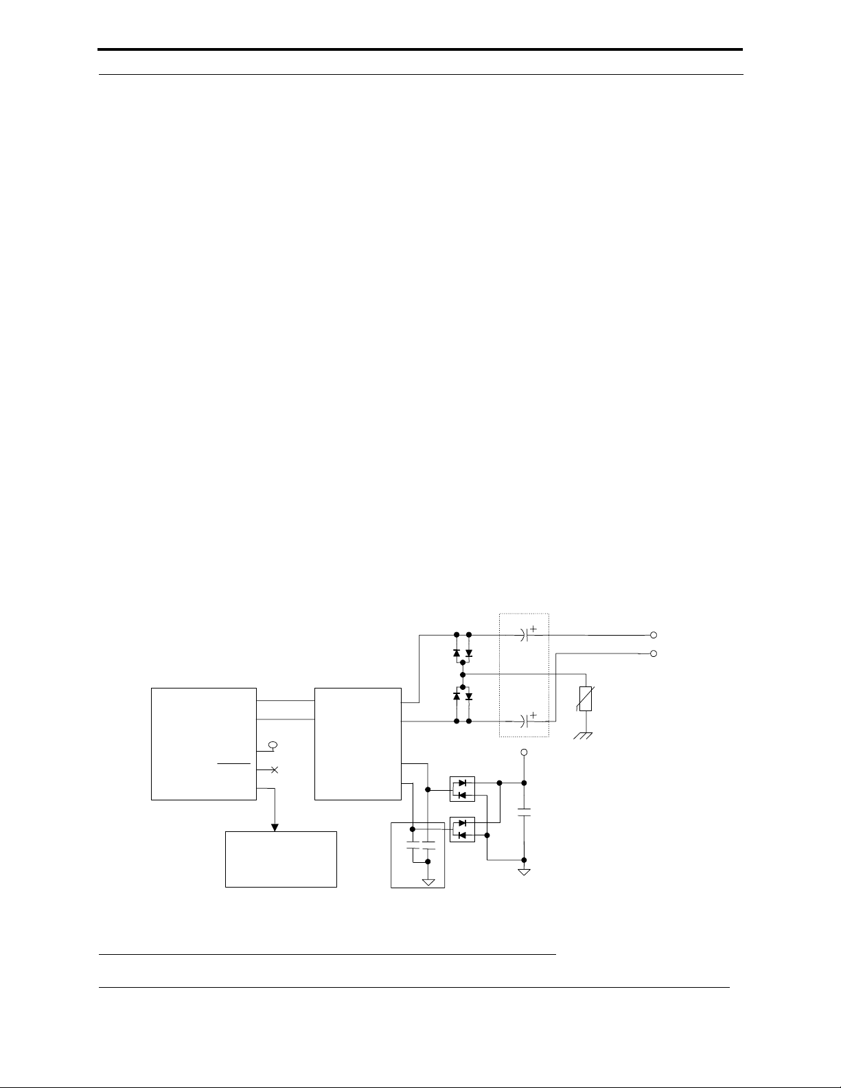
Interface between Smart Transceivers and the Network
The T1 and T2 signals are each brought out of the FT-X1 transformer at two different sets of pins. The T1 and T2
connections between the FT-X1 transformer and the FT Smart Transceivers can be made via either set of pins on
the FT-X1 transformer, but the connections shown in the PCB layout figures later in this chapter generally give the
best ESD transient immunity. T1 and T2 were used in FTT-10A transceiver-based designs for ESD clamping only,
but now they are also connected directly to the FT Smart Transceivers via the old RXD and TXD signals of the
Neuron Chip.
The FT-X2 transformer has only one set of T1 and T2 pins, corresponding to pins 5 and 6 on the FT-X1
transformer. Therefore, connection to FT Smart Transceivers, ESD protection circuitry, and C5/C6 capacitors are
all connected through the same set of T1 and T2 pins.
Since the T1 and T2 lines are analog connections between the FT Smart Transceiver and the FT-X1 transformer, no
other parallel connections should be made to these lines (other than the C5 and C6 capacitors and ESD protection
diodes shown in Figure 4.1), and no components should be placed in series between the FT Smart Transceiver and
the FT-X1or FT-X2 transformer. In particular, no RXD/TXD sensing circuitry should be attached to these lines.
There is now an explicit RXD/TXD signal available on the COMM_ACTIVE pin of the FT Smart Transceiver that
can be used for the purpose of driving RXD and TXD LEDs, if desired. See the following section for more
information about the COMM_ACTIVE LED drive circuit.
Interface between Smart Transceivers and the
Network
The preferred interconnection between the FT-X1 or FT-X2 transformer, an FT Smart Transceiver, and the
associated transient protection circuitry is shown in Figure 4.1. When using the FT-X1 transformer, pins 3 and 4 are
connected to the Smart Transceiver as shown in the figure, while ESD protection diodes are connected to pins 5
and 6. The FT-X2 transformer does not have pins 3 and 4. Connections to the Smart Transceiver and to the ESD
protection on FT-X2 are both done via pins 5 and 6. Figure 4.1 is not a complete schematic, since it does not
include the clock, reset, and power supply bypass circuits for the FT Smart Transceivers. Refer to the FT 3120 and
FT 3150 Smart Transceiver Datasheet for this additional information.
See
Text
FT 3120 Transceiver
FT 3150 Transceiver
(Partial)
T1
T2
RTMP
SLEEP
COMM_ACTIVE
COMM_ACTIVE
LED Drive Circuit
+5V
Optional
FT-X1 or FT-X2
Transformer*
3
T1
4
T2
*Use pins 5 & 6 for FT-X2
NET_A
NET_B
See
Text
T1
T2
C3
D3
D4
2
1
5
6
C5
C6
D5
D6
C4
+5V
D1
D2
C1
VR1
NET1
NET2
Figure 4.1 FT Smart Transceiver and FT-X1 or FT-X2 Interconnections with Transient Protection
Circuitry
FT 3120 / FT 3150 Smart Transceiver Data Book 93
Page 100

Chapter 4 - Hardware Design Considerations
Table 4.1 FT Smart Transceiver External Components
Name Val ue Comments
C1 0.1µF for +5VDC decoupling VCC decoupling capacitor for ESD protection
diodes D1-D2
VR1 470V MOV, 5mm, 40pF (typ.) Panasonic ERZV05D471, Digi-Key P7186-
ND or equivalent.
C3, C4
C5, C6 56pF, 5%, NPO or COG To enable EN61000-4-6 Level 3
D1, D2 BAV99, 1N414-equivalent ESD Transient clamping diodes
D3, D4, D5, D6
22µF, ≥50V, polar
BAV99, 1N4148-equivalent
1N4934, 1N4935, FR1D, RS1D,
RS1DB
DC blocking capacitors; see text
Differential network clamping diodes:
For up to 2kV Surge Protection
For up to 6kV Surge Protection
In Figure 4.1, capacitors C3 and C4 are used to provide DC voltage isolation for the FT Smart Transceiver when it is
used on a link power network or in the event of a DC power fault on the network wires. The capacitors are required to
meet L
ONMARK interoperability guidelines for the TP/FT-10 channel. These capacitors are not needed on devices that
will be connected exclusively to non-link power networks and do not require protection against DC faults. Two polar
capacitors are used to protect against the application of a DC voltage of either polarity, while providing a total
capacitance of 11µF. Alternatively, a single non-polar capacitor of 10µF may be used in either of the two legs which
connect to the network. The initial tolerance of the capacitor should be ±20% or less, and degradation due to aging
and temperature effects should not exceed 20% of the initial minimum value
Capacitors C5 and C6 are required on all new designs. They ensure that the FT Smart Transceivers support
EN61000-4-6 Level 3. Note that unlike the FTT-10A transceiver, the common mode noise immunity of the FT Smart
Transceivers is not significantly improved by the addition of the common mode choke specified in the L
ONWORKS
FTT-10A Free Topology Transceiver User’s Guide.
Figure 4.2 shows an example implementation of the optional COMM_ACTIVE LED drive circuit block that is
referred to in figure 4.1 on the previous page.
94 FT 3120 / FT 3150 Smart Transceiver Data Book
 Loading...