

Page 1

SX1262/SX1268 Wireless Module
E22 Series
This manual may be modified based on product upgrade, please refer to the latest version.
All rights to interpret and modify this manual belong to Chengdu Ebyte Electronic Technology Co., Ltd.
User Manual
Page 2
SX1262/SX1268 wireless module E22 series user manual
Copyright ©2012–2017,Chengdu Ebyte Electronic Technology Co.,Ltd.
1
Version
Date
Description
Issued by
1.00
2018/04/27
Initial version
huaa
1.10
2018/08/06
Modified version 01
Huaa
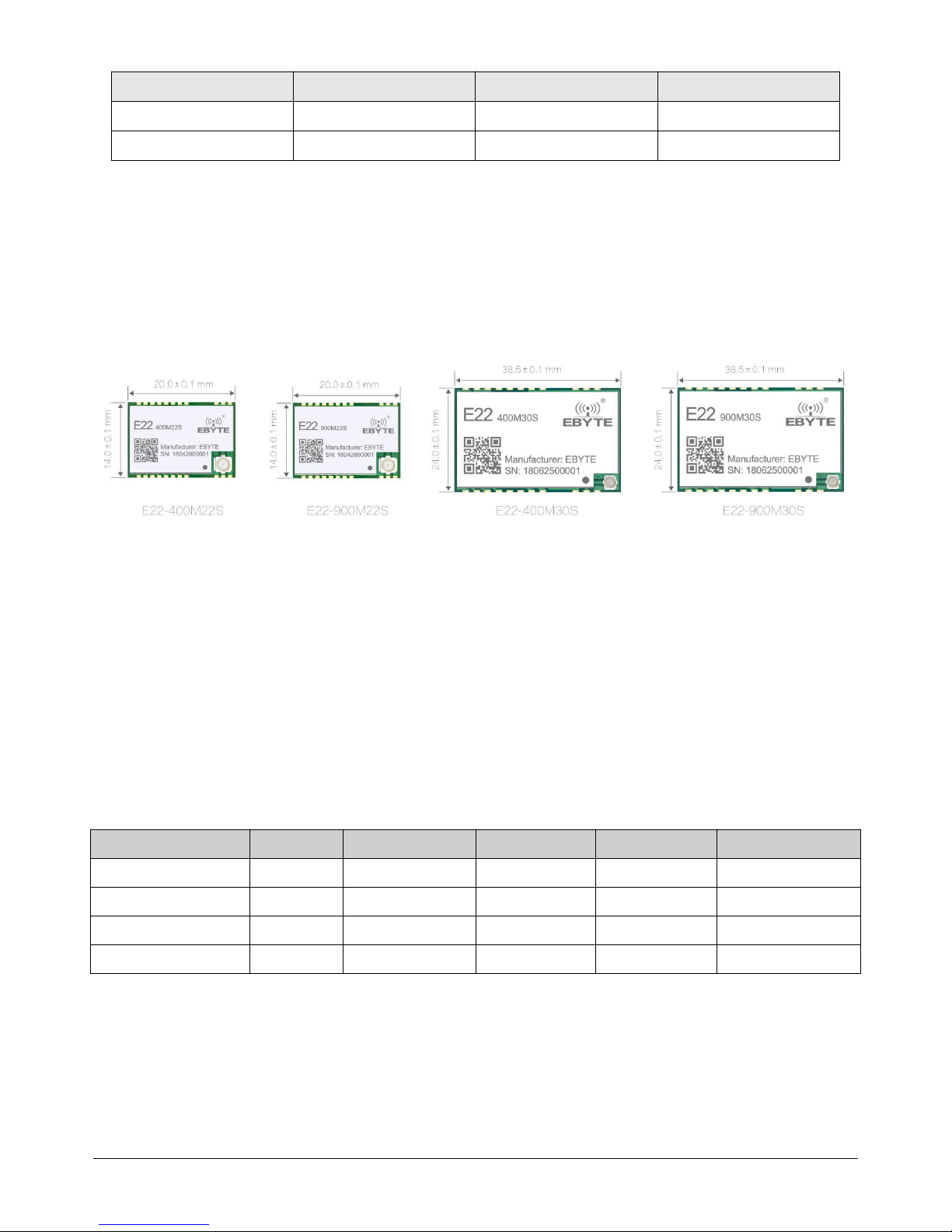
Brief Introduction
With multiple frequency band and wide frequency range , E22 series are small size (pin spacing :1.27mm) SMD wireless transceiver
module designed by Chengdu Ebyte. It features long range transmission and super low power consumption.
The E22 series is the first wireless module in China to adopt Semtech's SX1262, SX1268 RF chip. This chip provides a variety of
modulation methods, such as LoRaTM and traditional GFSK. Its special LoRaTM modulation method increases the communication
distance. At the same time, SX126x owns two distribution methods, low-dropout regulator (LDO) and high-efficiency step-down
DC-DC converter, under the premise of the choice of DC-DC mode, the receiving current is extremely low to achieve Low power
consumption. Compared with SX127x series, SX126x can achieve up to 62.5kbps air data rate in Lora mode. In GFSK mode, air data
rate can support up to 300kbps; according to the application of choice of power management, in the DC/DC mode, when in the
maximum power output of 22dBm The SX126x's power consumption is only 118mA, and the efficiency is improved significantly. The
SX126x RF receiver power consumption is 4.8mA, which is less than half of the SX127x series' 10mA receiving current.
E22 series strictly stick to the design rules home and abroad of FCC, CE, CCC and meet the related RF certifications and export
standards. As hardware platform, users need to carry out secondary development.
Model
Frequency
Transmitting power
Distance
Packing
Antenna
E22-400M22S
410-493MHz
22dBm
6500m
SMD
Stamp hole/IPEX
E22-900M22S
850-930MHz
22dBm
6500m
SMD
Stamp hole/IPEX
E22-400M30S
410-493MHz
30dBm
12000m
SMD
Stamp hole/IPEX
E22-900M30S
850-930MHz
30dBm
12000m
SMD
Stamp hole/IPEX
Page 3

SX1262/SX1268 wireless module E22 series user manual
Copyright ©2012–2017,Chengdu Ebyte Electronic Technology Co.,Ltd.
2
Contents
Brief Introduction
...........................................................................................................................................................................
1
1. Technical Parameter
..................................................................................................................................................................
3
1.1. E22-400M22S
.....................................................................................................................................................................
3
1.2. E22-900M20S
.....................................................................................................................................................................
3
1.3. E22-400M30S/ E22-900M30S
..........................................................................................................................................
4
1.4. Parameter descriptions
......................................................................................................................................................
4
2. Mechanical characteristic
..........................................................................................................................................................
5
2.1 E22-400M22S/E22-900M22S
............................................................................................................................................
5
2.1.1 Dimensions
....................................................................................................................................................................
5
2.1.2. Pin definition
................................................................................................................................................................
5
2.2 E22-400M30S/E22-900M30S
................................................................................................................................................
6
2.2.1 Dimensions
........................................................................................................................................................................
6
2.2.2 Pin definition
.....................................................................................................................................................................
7
3. Recommended Circuit Diagram
...............................................................................................................................................
8
3.1. E22-433M22S/E22-900M22S
............................................................................................................................................
8
3.2. E22-400M30S/E22-900M30S
............................................................................................................................................
8
4. Production Guidance
.................................................................................................................................................................
9
4.1. Reflow Soldering Temperature
..........................................................................................................................................
9
4.2. Reflow Curving Diagram
....................................................................................................................................................
9
5. FAQ
...........................................................................................................................................................................................
10
5.1. Communication range is too short
.................................................................................................................................
10
5.2. Module is easy to damage
..............................................................................................................................................
10
6. Important Notes
......................................................................................................................................................................
10
7. About Us
...................................................................................................................................................................................
10
Page 4
SX1262/SX1268 wireless module E22 series user manual
Copyright ©2012–2017,Chengdu Ebyte Electronic Technology Co.,Ltd.
3
1. Technical Parameter
Model
Core IC
Size
Net Weight
Operating
Temperature
Operating
Humidity
Storage
Temperature
E22-400M22S
SX1268
20* 14*2.8 mm
1.35±0.1 g
-40 ~ 85℃
10% ~ 90%
-40 ~ 125°C
E22-900M22S
SX1262
20* 14*2.8 mm
1.35±0.1 g
-40 ~ 85℃
10% ~ 90%
-40 ~ 125°C
E22-400M30S
SX1268
38.5* 24*3.6 mm
4.8±0.1g
-40 ~ 85℃
10% ~ 90%
-40 ~ 125°C
E22-900M30S
SX1262
38.5* 24*3.6 mm
4.64±0.1g
-40 ~ 85℃
10% ~ 90%
-40 ~ 125°C
1.1. E22-400M22S
Parameter
Min
Typ
Max
Unit
Tx current
(LoRa@2.4kbps)
95
100
105
mA
Rx current
(LoRa@2.4kbps)
4.6
4.8
5.7
mA
Turn-off current
150
180
200
nA
Tx power
21.4
21.5
22.3
dBm
Rx sensitivity
-144
-146
-147
dBm
TCXO323232MHz
TCXO voltage setting
1.8
1.8
3.3
V
Operating frequency
410
433/470/490
493
MHz
Voltage supply
1.8
3.3
3.7
V
Communication level
1.8
3.3
3.7
V
1.2. E22-900M20S
Parameter
Min
Typ
Max
Unit
Tx current
(LoRa@2.4kbps)
114
119
124
mA
Rx current
(LoRa@2.4kbps)
4.8
5.0
5.9
mA
Turn-off current
150
185
200
nA
Tx power
21.4
21.5
22.3
dBm
Rx sensitivity
-144
-146
-147
dBm
TCXO323232MHz
TCXO voltage setting
1.8
1.8
3.3
V
Operating frequency
850
868/915
930
MHz
Voltage supply
1.8
3.3
3.7
V
Communication level
1.8
3.3
3.7
V
Page 5

SX1262/SX1268 wireless module E22 series user manual
Copyright ©2012–2017,Chengdu Ebyte Electronic Technology Co.,Ltd.
4
1.3. E22-400M30S/ E22-900M30S
Parameter
Min
Typ
Max
Unit
Tx current
(LoRa@2.4kbps)
600
650
700
mA
Rx current
(LoRa@2.4kbps)
121416
mA
Turn-off current
1
35nA
Tx power
29.5
30.031dBm
Rx sensitivity
-149
-150
-151
dBm
TCXO
32
3232MHz
TCXO voltage setting
1.8
1.8
1.8
V
Operating frequency
410
433/470/490
493
MHz
Voltage supply
2.5
5
5.5
V
Communication level
1.8
3.3
3.7
V
1.4. Parameter descriptions
When designing the power supply circuit for the module, it is recommended to reserve more than 30% margin, and the whole machine is conducive
to long-term and stable operation.
The current required to launch at the moment is large but often because of the very short launch time, the total energy consumed may be smaller;
When users use an external antenna, the impedance matching between the antenna and the module at different frequency points will affect the
emission current to a different extent.
The current consumed when the radio frequency chip is in the pure receiving state is called the receiving current. Some radio frequency chips with
communication protocols or developers have loaded some of the self-developed protocols on the entire unit. This may cause the received current
to be large. ;
The currents in pure receiving state are often of the mA level, and for μA-level “receiving current”, developer need to process the software.
Shutdown current is often much less than the current consumed by the entire power supply when it is in no-load condition, and it is not excessively
demanding;
Because the material itself has a certain error, a single LRC component has an error of ±0.1%, but due to the use of multiple LRC components in the
entire RF loop, there will be an accumulation of errors, resulting in different emission current and receiving current of different modules. ;
Lowering the transmit power can reduce the power consumption to some extent, but reducing the transmit power emission due to many reasons
will reduce the efficiency of the internal PA.
Page 6

SX1262/SX1268 wireless module E22 series user manual
Copyright ©2012–2017,Chengdu Ebyte Electronic Technology Co.,Ltd.
5
2. Mechanical characteristic
2.1 E22-400M22S/E22-900M22S
2.1.1 Dimensions
2.1.2. Pin definition
Pin No.
Pin item
Pin direction
Pin application
1
GND
Ground
2
GND
Ground
3
GND
Ground
4
GND
Ground
5
GND
Ground
6
RXEN
Input
RF switch RX control,connecting external MCU IO, valid in high level
7
TXEN
Input
RF switch TX control,connecting external MCU IO or DIO2, valid in high level
8
DIO2
Input /output
Configurable IO port(see more in SX126x datasheet)
9
VCC
Power supply, 1.8V~3.7V(external ceramic filter capacitor is recommended)
10
GND
Ground
11
GND
Ground
Page 7

SX1262/SX1268 wireless module E22 series user manual
Copyright ©2012–2017,Chengdu Ebyte Electronic Technology Co.,Ltd.
6
12
GND
Ground
13
DIO1
Input /output
Configurable IO port(see more in SX126x datasheet)
14
BUSY
output
State indicator(see more in SX126x datasheet)
15
NRST
Input
Chip reset initiation, valid in low level
16
MISO
output
SPI master input slave output
17
MOSI
Input
SPI master output slave input
18
SCK
Input
SPI clock
19
NSS
Input
Chip select,for starting a SPI communication
20
GND
Ground
21
ANT
Stamp hole(50 ohm impedance)
22
GND
Ground
★ Find more details on《SX126x Datasheet》from Semtech ★
2.2 E22-400M30S/E22-900M30S
2.2.1 Dimensions
Page 8

SX1262/SX1268 wireless module E22 series user manual
Copyright ©2012–2017,Chengdu Ebyte Electronic Technology Co.,Ltd.
7
2.2.2 Pin definition
Pin No.
Pin item
Pin direction
Pin application
1
GND
Ground
2
GND
Ground
3
GND
Ground
4
GND
Ground
5
GND
Ground
6
RXEN
Input
RF switch RX control,connecting external MCU IO, valid in high level
7
TXEN
Input
RF switch TX control,connecting external MCU IO or DIO2, valid in high level
8
DIO2
Input /Output
Configurable IO port(see more in SX126x datasheet)
9
VCC
Power supply, 2.5V~5.5V(external ceramic filter capacitor is recommended)
10
VCC
Power supply, 2.5V~5.5V(external ceramic filter capacitor is recommended)
11
GND
Ground
12
GND
Ground
13
DIO1
Input /Output
Configurable IO port(see more in SX126x datasheet)
14
BUSY
Output
State indicator(see more in SX126x datasheet)
15
NRST
Input
Chip reset initiation, valid in low level
16
MISO
Output
SPI master input slave output
17
MOSI
Input
SPI master output slave input
18
SCK
Input
SPI clock
19
NSS
Input
Chip select,for starting a SPI communication
20
GND
Ground
21
ANT
Stamp hole(50 ohm impedance)
22
GND
Ground
★ Find more details on《SX126x Datasheet》from Semtech ★
Page 9

SX1262/SX1268 wireless module E22 series user manual
Copyright ©2012–2017,Chengdu Ebyte Electronic Technology Co.,Ltd.
8
3. Recommended Circuit Diagram
3.1. E22-433M22S/E22-900M22S
3.2. E22-400M30S/E22-900M30S
Page 10

SX1262/SX1268 wireless module E22 series user manual
Copyright ©2012–2017,Chengdu Ebyte Electronic Technology Co.,Ltd.
9
NO.
Instruction for connection between module and MCU
1
IO0, IO1, IO2, IO3 means IO ports of MCU.
2
DIO1、DIO2 are GPIO,configurable for multiple functions;DIO2 can connect to TXEN,without connecting to IO of MCU,for controlling RF switch TX, Please
see more in SX126x datasheet, can be floated when free.
3
E22(433M22S) uses DIO3 internally to power 32MHz TCXO.
4
Well grounded with large area for grounding,small power ripple, filter capacitor should be installed and near to VCC and GND.
5
E22(400M30S):It is recommended to add a 200R protection resistor to the RXD/TXD of the external MCU.
4. Production Guidance
4.1. Reflow Soldering Temperature
Profile Feature
Sn-Pb Assembly
Pb-Free Assembly
Solder Paste
Sn63/Pb37
Sn96.5/Ag3/Cu0.5
Preheat Temperature min (Tsmin)
100℃
150℃
Preheat temperature max (Tsmax)
150℃
200℃
Preheat Time (Tsmin to Tsmax)(ts)
60-120 sec
60-120 sec
Average ramp-up rate(Tsmax to Tp)
3℃/second max
3℃/second max
Liquidous Temperature (TL)
183℃
217℃
Time(tL)Maintained Above(TL)
60-90 sec
30-90 sec
Peak temperature(Tp)
220-235℃
230-250℃
Aveage ramp-down rate(Tp to Tsmax)
6℃/second max
6℃/second max
Time 25℃ to peak temperature
6 minutes max
8 minutes max
4.2. Reflow Curving Diagram
Page 11

SX1262/SX1268 wireless module E22 series user manual
Copyright ©2012–2017,Chengdu Ebyte Electronic Technology Co.,Ltd.
10
5. FAQ
5.1. Communication range is too short
The communication distance will be affected when obstacle exists.
Data lose rate will be affected by temperature, humidity and co-channel interference.
The ground will absorb and reflect wireless radio wave, so the performance will be poor when testing near ground.
Seawater has great ability in absorbing wireless radio wave, so performance will be poor when testing near the sea.
The signal will be affected when the antenna is near metal object or put in a metal case.
Power register was set incorrectly, air data rate is set as too high (the higher the air data rate, the shorter the distance).
The power supply low voltage under room temperature is lower than 2.5V, the lower the voltage, the lower the transmitting power.
Due to antenna quality or poor matching between antenna and module.
5.2. Module is easy to damage
Please check the power supply source, ensure it is within the recommended value, voltage higher than that will damage the module.
Please check the stability of power source, the voltage cannot fluctuate too much.
Please make sure antistatic measure are taken when installing and using, high frequency devices have electrostatic susceptibility.
Please ensure the humidity is within limited range, some parts are sensitive to humidity.
Please avoid using modules under too high or too low temperature.
6. Important Notes
All rights to interpret and modify this manual belong to Ebyte.
This manual will be updated based on the upgrade of firmware and hardware, please refer to the latest version.
Please refer to our website for new product information
7. About Us
Technical support: support@cdebyte.com
Documents and RF Setting download link: www.cdebyte.com/en/
Tel:+86-28-61399028 Ext. 812
Fax:028-64146160
Web:www.cdebyte.com/en/
Address:Innovation Center D347, 4# XI-XIN Road,Chengdu, Sichuan, China
 Loading...