

Page 1

nRF52832/nRF52810/nRF52840/nRF51822
Wireless Module
E73 Series
This manual may be modified based on product upgrade, please refer to the latest version.
All rights to interpret and modify this manual belong to Chengdu Ebyte Electronic Technology Co., Ltd.
User Manual
Page 2
Copyright ©2012–2017,Chengdu Ebyte Electronic Technology Co., Ltd. 1
Version
Date
Description
Issued by
1.00
2017/12/06
Initial version
huaa
1.10
2017/12/06
Name changed
huaa
1.20
2018/05/23
Content added
Huaa
1.30
2018/08/01
E73(2G4M08S1C) added
Huaa
Brief Introduction
E73 series are wireless Bluetooth modules designed by Chengdu Ebyte which feature small size, low power consumption, built in PCB
antenna and IPX interface. E73 series adopt the originally imported RFIC nRF52832/ nRF52810/nRF52840 of NORDIC, supporting BLE 4.2
and BLE 5.0. The chip has high-performance ARM CORTEX-M4F kernel and other peripheral resources, such as UART, I2C, SPI, ADC, DMA,
PWM etc. The module led out all the IO port of nRF52832/nRF52810 and most IO Port of nRF52840 for multilateral development. For more
details, please refer to the datasheet of NORDIC. For E73 (2G4M04S1D), We used 16MHz high precision low temperature drift active
crystal oscillator and other model used 32MHz crystal oscillator, which ensure its industrial characteristics and stability performance
Compared with Bluetooth 4.2, Bluetooth 5 has the following advantages: 2x air data bandwidth(2Mbps), The broadcasting capacity is
increased(x8). Broadcasting extension makes the data length increase to 251 bytes which enables more effective data transmission in
beacon applications. 5210 applies S112 protocol stack which has been strictly tested and upgraded. It supports 196kB Flash/24kB RAM of
nRF52810 SoCs. S112 protocol stack only take 100kbB flash which means it saves enough space for massive low consumption Bluetooth
applications and provides reliable support for upgrade for OTA applications.
E73 series are hardware platform without firmware, so users need to conduct a secondary development. This series have maximized
the RF characteristics of chip. The built-in 32.768K real-time clock crystal oscillator can benefit users in programming(Note:
E73(2G4M08S1C) did not built in the crystal oscillator.)
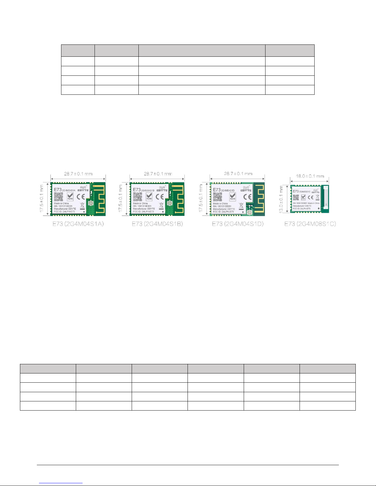
Model
Frequency
Transmitting power
Distance(PCB/IPX)
Packing
Antenna
E73 (2G4M04S1B)
2.4GHz
4dBm
100m
SMD
PCB/IPX
E73 (2G4M04S1A)
2.4GHz
4dBm
110m
SMD
PCB/IPX
E73 (2G4M04S1D)
2.4GHz
4dBm
110m
SMD
PCB/IPX
E73(2G4M08S1C)
2.4GHz
8dBm
120m
SMD
Ceramic antenna
Page 3

Copyright ©2012–2017,Chengdu Ebyte Electronic Technology Co., Ltd. 2
目录
1.
Technical Parameter
....................................................................................................................................................................
4
1.1. Internal resources
..............................................................................................................................................................
4
1.2. E73 (2G4M04S1B)
..............................................................................................................................................................
4
1.3. E73 (2G4M04S1A)
.............................................................................................................................................................
4
1.4. E73 (2G4M04S1D)
.............................................................................................................................................................
5
1.5. E73(2G4M08S1C)
...............................................................................................................................................................
5
1.6. Parameter notes
................................................................................................................................................................
5
2. Mechanical Properties
................................................................................................................................................................
6
2.1. E73 (2G4M04S1B)/E73 (2G4M04S1A)
.........................................................................................................................
6
2.1.1. Dimension
.................................................................................................................................................................
6
2.1.2 Pin Definition
............................................................................................................................................................
6
2.2. E73 (2G4M04S1D)
.............................................................................................................................................................
8
2.2.1. Dimension
.................................................................................................................................................................
8
2.3. E73(2G4M08S1C)
...............................................................................................................................................................
9
2.3.1 dimension
..................................................................................................................................................................
9
2.3.2 Pin definition
...........................................................................................................................................................
10
3. Development and Application
...............................................................................................................................................
11
4. Antenna Type
..............................................................................................................................................................................
11
4.1. E73 (2G4M04S1A)/E73 (2G4M04S1B)
.......................................................................................................................
11
4.2. E73 (2G4M04S1D)
...........................................................................................................................................................
11
5. Production Guidance
................................................................................................................................................................
12
5.1. Reflow Soldering Temperature
...................................................................................................................................
12
5.2. Reflow Soldering Curve
.................................................................................................................................................
12
6. FAQ
................................................................................................................................................................................................
13
Page 4

Copyright ©2012–2017,Chengdu Ebyte Electronic Technology Co., Ltd. 3
6.1. Communication range is too short
............................................................................................................................
13
6.2. Module is easy to damage
...........................................................................................................................................
13
6.3. Burn firmware
...................................................................................................................................................................
13
7. Schematic Diagram
...................................................................................................................................................................
14
7.1. E73 (2G4M04S1A)
...........................................................................................................................................................
14
7.2. E73 (2G4M04S1B)
...........................................................................................................................................................
14
7.3. E73 (2G4M04S1D)
...........................................................................................................................................................
15
7.4. E73 (2G4M08S1C)
...........................................................................................................................................................
15
8. Important Notes
........................................................................................................................................................................
16
9. About Us
......................................................................................................................................................................................
16
Page 5
Copyright ©2012–2017,Chengdu Ebyte Electronic Technology Co., Ltd. 4
1. Technical Parameter
Model
IC
Antenna
Size
Net weight
Operating
temperature
Operating
humidity
Storage
temperature
E73 (2G4M04S1B)
nRF52832-QFAA
PCB/IPX
17.5 * 28.7 mm
1.8±0.1g
-40 ~ 85℃
10% ~ 90%
-40 ~ 125°C
E73 (2G4M04S1A)
nRF52810-QFAA
PCB/IPX
17.5 * 28.7 mm
1.8±0.1g
-40 ~ 85℃
10% ~ 90%
-40 ~ 125°C
E73 (2G4M04S1D)
nRF51822
PCB/IPX
17.5 * 28.7 mm
1.8±0.1g
-40 ~ 85℃
10% ~ 90%
-40 ~ 125°C
E73(2G4M08S1C)
nRF52840-QIAAC0
Ceramic antenna
13*18*0.8mm
1.02±0.1g
-40 ~ 85℃
10% ~ 90%
-40 ~ 125°C
1.1. Internal resources
Model
IC
FLASH
RAM
Core
E73(2G4M04S1B)
nRF52832-QFAA/QFN48
512KB
64KB
ARM® Cortex™-M4F
E73(2G4M04S1A)
nRF52810-QFAABB/QFN48
192KB
24KB
ARM Cortex®-M4
E73 (2G4M04S1D)
nRF51822-QFAA/QFN48
256KB
16KB
ARM® Cortex™ M0
E73(2G4M08S1C)
nRF52840-QIAAC0/ aQFN ™ 73
1024KB
256KB
ARM® Cortex ® -M4
1.2. E73 (2G4M04S1B)
Parameter
Min
Type
Max
Unit
Transmitting current
13
1415mA
Receiving current
456
mA
Turn-off current
1
23μA
Transmitting power
3.8
4
4.3
dBm
Receiving sensitivity
-94
-95
-96
dBm
Recommended band
2379
2430
2496
MHz
Voltage supply
1.8
3.3
3.6
V
Communication level
1.8
3.3
3.6
V
1.3. E73 (2G4M04S1A)
Parameter
Min
Typ
Max
Unit
Transmitting current
171820
mA
Receiving current
121314
mA
Turn-off current
123
μA
Transmitting power
3.744.2
dBm
Receiving sensitivity
-94
-95
-96
dBm
Recommended band
2379
2430
2496
MHz
Voltage supply
1.8
3.3
3.6
V
Communication level
1.8
3.3
3.6
V
Page 6
Copyright ©2012–2017,Chengdu Ebyte Electronic Technology Co., Ltd. 5
1.4. E73 (2G4M04S1D)
Parameter
Min
Typ
Max
Unit
Transmitting current
13.0
14.0
15.4
mA
Receiving current
11.3
12.6
13.8
mA
Turn-off current
0.5
1.0
2.5
μA
Transmitting power
3.6
4.0
4.5
dBm
Receiving sensitivity
-95.4
-96.0
-96.8
dBm
Recommended band
2379
2430
2496
MHz
Voltage supply
2.1
3.3
3.6
V
Communication level
2.1
3.3
3.6
V
1.5. E73(2G4M08S1C)
Parameter
Condition
Min
Typ
Max
Unit
Transmitting current
TX only run current (DC/DC, 3 V) PRF= +8 dBm
17.05
mA
TX only run current (DC/DC, 3 V) PRF= +4 dBm
12.68
TX only run current (DC/DC, 5 V, REG0 out = 3.3 V)PRF= 0dBm
7.25
TX only run current (DC/DC, 3 V)P RF = 0 dBm
7.63
Receiving current
RX only run current (DC/DC, 3 V) 1 Mbps / 1 Mbps BLE
7.71
mA
RX only run current (DC/DC, 3 V) 2 Mbps / 2 Mbps BLE
8.27
Transmitting power
-
7
dBm
Receiving sensitivity
-
-103 dBm@BLE 125kbps(long distance mode)、 -95 dBm@BLE 1M
dBm
Recommended band
-
2360
2402
24500
MHz
Voltage supply
-
1.7
3.3
5.5
V
Communication level
-
0.7 X VDD
VDD
V
Note: The current is the current of the whole machine. 64 MHz CPU clock, 52 μA/MHz running from flash memory.
1.6. Parameter notes
1 When designing current supply circuit, 30% margin is recommended to be remained so as to ensure long-term stable operation of
the whole module.
2. The current at the instant of transmitting may be high, but the total energy consumed may be lower due to very short transmitting
time.
3. When using external antenna, the impedance matching degree at different frequency points between antenna and module may
affect the transmitting current at different levels.
4. The current consumed when the RF chip is only working at receiving mode is called as receiving current. The tested receiving current
may be higher for some RF chips with communication protocol or when the developers have loaded their own protocol to the whole
module.
5. The current at pure receiving mode is at mA level. To achieve µA level receiving current, the users need to manage it through
firmware development.
6. The turn-off current is always lower than the current consumed when the power supply source of the whole module is at no-load
status.
7. Each LRC component has ±0.1% error, and the error will accumulate since multiple LRC components are used in the whole RF circuit,
and the transmitting current will be different at different modules.
8. The power consumption can be lowered by lowering the transmitting power, but the efficiency of the internal PA will be decreased
by lowering transmitting power due to various reasons
Page 7

Copyright ©2012–2017,Chengdu Ebyte Electronic Technology Co., Ltd. 6
2. Mechanical Properties
2.1. E73 (2G4M04S1B)/E73 (2G4M04S1A)
2.1.1. Dimension
2.1.2. Pin Definition
No.
Pin item
Pin direction
Application
0
GND
Input
Ground electrode, connect to reference ground of power
1
GND
Input
Ground electrode, connect to reference ground of power
2
GND
Input
Ground electrode, connect to reference ground of power
3
DEC2
1.3 V Digital power supply decoupling controller
4
DEC3
Power supply decoupling
5
P0.25
Input/Output
MCU GPIO6P0.26
Input/Output
MCU GPIO
7
P0.27
Input/Output
MCU GPIO
8
P0.28
Input/Output
MCU GPIO
9
P0.29
Input/Output
MCU GPIO
10
P0.30
Input/Output
MCU GPIO
Page 8

Copyright ©2012–2017,Chengdu Ebyte Electronic Technology Co., Ltd. 7
11
P0.31
Input/Output
MCU GPIO
12
DEC4
1.3 V Digital power supply decoupling controller
Input from DC/DC regulator Output from1.3 V LDO
13
DCC
DC/DC DC regulator output
14
DEC1
0.9 V Digital power supply decoupling controller
15
GND
Input
MCU GPIO
16
VCC
Input
Power supply 1.8 ~ 3.6V DC(Note: The voltage higher 3.6V is forbidden)
17
P0.02
Input/Output
MCU GPIO
18
P0.03
Input/Output
MCU GPIO
19
P0.04
Input/Output
MCU GPIO
20
P0.05
Input/Output
MCU GPIO
21
P0.06
Input/Output
MCU GPIO
22
P0.07
Input/Output
MCU GPIO
23
P0.08
Input/Output
MCU GPIO
24
P0.09
Input/Output
MCU GPIO
25
P0.10
Input/Output
MCU GPIO
26
P0.11
Input/Output
MCU GPIO
27
P0.12
Input/Output
MCU GPIO
28
P0.13
Input/Output
MCU GPIO
29
P0.14
Input/Output
MCU GPIO
30
P0.15
Input/Output
MCU GPIO
31
P0.16
Input/Output
MCU GPIO
32
P0.17
Input/Output
MCU GPIO
33
P0.18
Input/Output
MCU GPIO
34
P0.19
Input/Output
MCU GPIO
35
P0.20
Input/Output
MCU GPIO
36
P0.21
Input/Output/RST
MCU GPIO
37
SWDCLK
Input
Serial Line Debugging / Clock Input Debugging and Programming
38
SWDIO
Input
Serial line debugging and programming debugging
39
P0.22
Input/Output
MCU GPIO
40
P0.23
Input/Output
MCU GPIO
41
P0.24
Input/Output
MCU GPIO
42
GND
Input
Ground electrode, connect to power reference ground
43
GND
Input
Ground electrode, connect to power reference ground
★ For more details, please refer to《nRF528XXDatasheet》in NORDIC ★
Page 9

Copyright ©2012–2017,Chengdu Ebyte Electronic Technology Co., Ltd. 8
2.2. E73 (2G4M04S1D)
2.2.1. Dimension
No.
Pin item
Pin direction
Application
1
P0.21
Input/Output
MCU GPIO
2
P0.22
Input/Output
MCU GPIO
3
P0.23
Input/Output
MCU GPIO
4
P0.24
Input/Output
MCU GPIO
5
P0.25
Input/Output
MCU GPIO
6
P0.28
Input/Output
MCU GPIO
7
P0.29
Input/Output
MCU GPIO
8
P0.30
Input/Output
MCU GPIO
9
P0.00
Input/Output
MCU GPIO
10
P0.01
Input/Output
MCU GPIO
11
VCC
Power supply 2.1 ~ 3.6V DC(Note: The voltage higher 3.6V is forbidden)
12
GND
Ground electrode, connect to power reference ground
13
GND
Ground electrode, connect to power reference ground
14
P0.02
0.9 V Digital power supply decoupling controller
15
P0.03
Input/Output
MCU GPIO
16
P0.04
Input/Output
MCU GPIO
17
P0.05
Input/Output
MCU GPIO
18
P0.06
Input/Output
MCU GPIO
Page 10

Copyright ©2012–2017,Chengdu Ebyte Electronic Technology Co., Ltd. 9
19
P0.07
Input/Output
MCU GPIO
20
P0.08
Input/Output
MCU GPIO
21
P0.09
Input/Output
MCU GPIO
22
P0.10
Input/Output
MCU GPIO
23
P0.11
Input/Output
MCU GPIO
24
GND
Input/Output
MCU GPIO
25
GND
Input/Output
MCU GPIO
26
P0.12
Input/Output
MCU GPIO
27
P0.13
Input/Output
MCU GPIO
28
P0.14
Input/Output
MCU GPIO
29
P0.15
Input/Output
MCU GPIO
30
P0.16
Input/Output
MCU GPIO
31
SWDIO/ nRESET
Input
Serial line debugging and programming debugging / MCU reset, low level enable
32
SWDCLK
Input
Serial Line Debugging / Clock Input Debugging and Programming
33
P0.17
Input/Output
MCU GPIO
34
P0.18
Input/Output
MCU GPIO
35
P0.19
Input/Output
MCU GPIO
36
P0.20
Input/Output
MCU GPIO
★ For more details, please refer to《nRF51822Datasheet》in NORDIC ★
2.3. E73(2G4M08S1C)
2.3.1 dimension
Page 11

Copyright ©2012–2017,Chengdu Ebyte Electronic Technology Co., Ltd. 10
2.3.2 Pin definition
No.
Pin item
Pin direction
Application
No.
1
P1.11
-
Common I/O
-
2
P1.10-Common I/O
Low frequency I/O, standard drive
3
P0.03
P0.03/AIN1
Common I/O
Analog input 1, low frequency I/O, standard drive
4
AI4
P0.28/AIN4
Common I/O
Analog input 4
5
GND--
Single ground line,connect to the power reference ground
6
P1.13-Common I/O
Low frequency I/O, standard drive
7
AI0
P0.02/AIN0
Common I/O
Analog input 0, low frequency I/O, standard drive
8
AI5
P0.29/AIN5
Common I/O
Analog input 5, low frequency I/O, standard drive
9
AI7
P0.31/AIN7
Common I/O
Analog input 7, low frequency I/O, standard drive
10
AI6
P0.30/AIN6
Common I/O
Analog input 6, low frequency I/O, standard drive
11
XL1
P0.00/XL1
Common I/O
Connect to 32.768 kHz crystal
12
P0.26-Common I/O
-
13
XL2
P0.01/XL2
Common I/O
Connect to 32.768 kHz crystal
14
P0.06-Common I/O
-
15
AI3
P0.05/AIN3
Common I/O
Analog input 3
16
P0.08-Common I/O
-
17
P1.09-Common I/O
-
18
AI2
P0.04/AIN2
Common I/O
Analog input 2
19
VDD--
Power supply
20
P12
P0.12
Common I/O
-
21
GND--
ground line,connect to the power reference ground
22
P0.07-Common I/O
-
23
VDH
VDDH
-
High-voltage power supply
24
GND--
ground line,connect to the power reference ground
25
DCH
DCCH
-
DC/DC Converter output
26
RST
P0.18/RESET
Common I/O
QSPI/CSN/ external reset
27
VBS
VBUS
-
USB power supply,5V input,used to USB3.3V voltage regulator
28
P15
P0.15
Common I/O
-
29D--
-
USB D-
30
P17
P0.17
Common I/O
-
31
D+--
USB D+
32
P0.20-Common I/O
-
33
P0.13-Common I/O
-
34
P0.22-Common I/O
QSPI
35
P0.24-Common I/O
QSPI
36
P1.00-Common I/O
-
37
SWD
SWDIO
-
Serial debug programming port data
38
P1.02-Common I/O
-
39
SWC
SWDCLK
-
Serial debug programming port clock
40
P1.04-Common I/O
Low frequency I/O, standard drive
41
NF1
P0.09/NFC1
Common I/O
NFC input
42
P1.06-Common I/O
Low frequency I/O, standard drive
43
NF2
P0.10/NFC2
Common I/O
NFC input
★ For more details, please refer to《nRF52840Datasheet》in NORDIC ★
Page 12

Copyright ©2012–2017,Chengdu Ebyte Electronic Technology Co., Ltd. 11
3. Development and Application
No.
Item
Notes
1
Burn Firmware
1.The module is embedded with ARM MCU. For program downloading, please use the J-LINK
downloader. Any other serial port or JTAG、ISP、ICP are unavailable to download.
2.There are two ways to download the program. The protocol stack of NORDIC is not programmed yet,
so users need to use the official nRFgo studio of NORDIC to program the protocol stack first, then
program the hex of application code. Or, to program the protocol stack of NORDIC first and download
via the IAR or KEIL. Website of tool download:
http://www.nordicsemi.com/eng/Products/Bluetooth-low-energy/nRF52832/(language)/eng-GB
2
Testing Board
Testing board is not available.
4. Antenna Type
4.1. E73 (2G4M04S1A)/E73 (2G4M04S1B)
The default 0R resistance welding as shown above(left), antenna type is PCB. If users need to change it to IPEX, pls make the 0R
resistance as show above(right)
4.2. E73 (2G4M04S1D)
The default 0R resistance welding as shown above(left), antenna type is PCB. If users need to change it to IPEX, pls make the 0R
resistance as show above(right)
Page 13

Copyright ©2012–2017,Chengdu Ebyte Electronic Technology Co., Ltd. 12
5. Production Guidance
5.1. Reflow Soldering Temperature
Profile Feature
Curve feature
Sn-Pb Assembly
Pb-Free Assembly
Solder Paste
Solder paste
Sn63/Pb37
Sn96.5/Ag3/Cu0.5
Preheat Temperature min (Tsmin)
Minimum preheating temperature
100℃
150℃
Preheat temperature max (Tsmax)
Maximum preheating temperature
150℃
200℃
Preheat Time (Tsmin to Tsmax)(ts)
Preheating time
60-120 sec
60-120 sec
Average ramp-up rate(Tsmax to Tp)
Average rising rate
3℃/second max
3℃/second max
Liquidous Temperature (TL)
Liquid phase temperature
183℃
217℃
Time(tL)Maintained Above(TL)
Time above liquidus
60-90 sec
30-90 sec
Peak temperature(Tp)
Peak temperature
220-235℃
230-250℃
Aveage ramp-down rate(Tp to Tsmax)
Average descent rate
6℃/second max
6℃/second max
Time 25℃ to peak temperature
Time of 25 ° C to peak temperature
6 minutes max
8 minutes max
5.2. Reflow Soldering Curve
Page 14

Copyright ©2012–2017,Chengdu Ebyte Electronic Technology Co., Ltd. 13
6. FAQ
6.1. Communication range is too short
The communication distance will be affected when obstacle exists.
Data lose rate will be affected by temperature, humidity and co-channel interference.
The ground will absorb and reflect wireless radio wave, so the performance will be poor when testing near ground.
Sea water has great ability in absorbing wireless radio wave, so performance will be poor when testing near the sea.
The signal will be affected when the antenna is near metal object or put in a metal case.
Power register was set incorrectly, air data rate is set as too high (the higher the air data rate, the shorter the distance).
When the power supply at room temperature is lower than the recommended low voltage, the lower the voltage is, the lower the
transmitting power is.
Due to antenna quality or poor matching between antenna and module.
6.2. Module is easy to damage
Please check the power supply and ensure it is within the recommended range. Voltage higher than the peak will lead to a
permanent damage to the module.
Please check the stability of power supply and ensure the voltage not to fluctuate too much.
Please make sure anti-static measures are taken when installing and using, high frequency devices have electrostatic susceptibility.
Please ensure the humidity is within limited range for some parts are sensitive to humidity.
Please avoid using modules under too high or too low temperature.
6.3. Burn firmware
Because of the bad compatibility of nRFgo Studio,We’d like to recommend users to choose J-LINK-V8 or above version for
programming.
About the issue that the old module can be programmed while the new one cannot, it’s because we added the read-write
protection in the production of new module. Users need to connect it correctly and then use the official nRFgo Studio to recover
(Jlink supports official nRFgo Studio ), as below:
Page 15

Copyright ©2012–2017,Chengdu Ebyte Electronic Technology Co., Ltd. 14
7. Schematic Diagram
7.1. E73 (2G4M04S1A)
7.2. E73 (2G4M04S1B)
Page 16

Copyright ©2012–2017,Chengdu Ebyte Electronic Technology Co., Ltd. 15
7.3. E73 (2G4M04S1D)
Note: DC/DC as the default. Mass customization available for LDO mode.
7.4. E73 (2G4M08S1C)
Page 17

Copyright ©2012–2017,Chengdu Ebyte Electronic Technology Co., Ltd. 16
Note: DC/DC as the default. Mass customization available for LDO mode.. Power supply is 17-5.5V.
Modules led out VDD,VDDH,DCCH pin, Please refer to the official manual for power supply.
Power supply mode:
normal voltage mode:1.7-3.6V. VDD=VDDH= Power supply,DCCH is floating,see more details in official manual.
high voltage mode:2.5-5.5V. DCCH=VDD(DCCH and VDD are connected via 10uH ±20%/ 80mA inductance),VDDH= Power supply,
see more details in official manual.
8. Important Notes
All rights to interpret and modify this manual belong to Ebyte.
This manual will be updated based on the upgrade of firmware and hardware, please refer to the latest version.
Please refer to our website for new product information.
9. About Us
Technical support: support@cdebyte.com
Documents and RF Setting download link: www.cdebyte.com/en/
Tel:+86-28-61399028
Fax:028-64146160
Web:www.cdebyte.com/en/
Address:Innovation Center D347, 4# XI-XIN Road, Gaoxin District(west), Chengdu, Sichuan,China.
 Loading...