

Ebyte E10 Series, E10-433MS, E10-433MS1W, E10-868M20, E10-868M30 User Manual
...
SI4463 Wireless Module
User Manual
E10 Series
This manual may be modified based on product upgrade, please refer to the latest version.
All rights to interpret and modify this manual belong to Chengdu Ebyte Electronic Technology Co., Ltd.
SI4463 wireless module E10 series user manual
Version
Date
Description
Issued by
1.00
2017/10/27
Initial version
huaa
Model
Antenna
Packing
Transmitting power
Distance
E10-433MS
Stamp hole
SMD
20dBm
2000m
E10-433MS1W
Stamp hole
SMD
30dBm
6000m
E10-868M20
Stamp hole/IPX
SMD
20dBm
2000m
E10-868M30
Stamp hole/IPX
SMD
30dBm
6000m
E10-915M20
Stamp hole/IPX
SMD
20dBm
2000m
E10-915M30
Stamp hole/IPX
SMD
30dBm
6000m
Brief Introduction
Based on originally imported RF IC SI4463 form Silicon Labs, E10 series are small size Sub-1GHz SMD wireless transceiver module, with SPI interface
and 26M crystal oscillator, developed by Chengdu Ebyte. The 30dBm module with PA and LNA, the communication stability and distance are largely
improved.
E10 series strictly stick to the design rules home and abroad of FCC, CE, CCC and meet the related RF certifications and export standards. As
hardware platform,, users need to carry out secondary development.
Copyright ©2012–2017,Chengdu Ebyte Electronic Technology Co.,Ltd.
1

SI4463 wireless module E10 series user manual
Contents
BRIEF INTRODUCTION
1. 1.TECHNICAL PARAMETER
1.1. GENERAL PARAMETER
1.2. ELECTRICAL PARAMETER
1.2.1. Transmitting current
1.2.2. Receiving current
1.2.3. Turn-off current
1.2.4. Voltage supply
1.2.5. Communication level
1.3. RF PARAMETER
1.3.1. Transmitting power
1.3.2. Receiving Sensitivity
......................................................................................................................................................................
..........................................................................................................................................................
....................................................................................................................................................................
.................................................................................................................................................................
............................................................................................................................................................
.................................................................................................................................................................
...................................................................................................................................................................
.....................................................................................................................................................................
...........................................................................................................................................................
..............................................................................................................................................................................
.............................................................................................................................................................
............................................................................................................................................................
1.3.3. Recommended operating frequency
1.4. TESTED DISTANCE
2. MECHANICAL CHARACTERISTICS
..........................................................................................................................................................................
.................................................................................................................................
..............................................................................................................................................
1
3
3
3
3
3
3
4
4
4
4
4
5
5
6
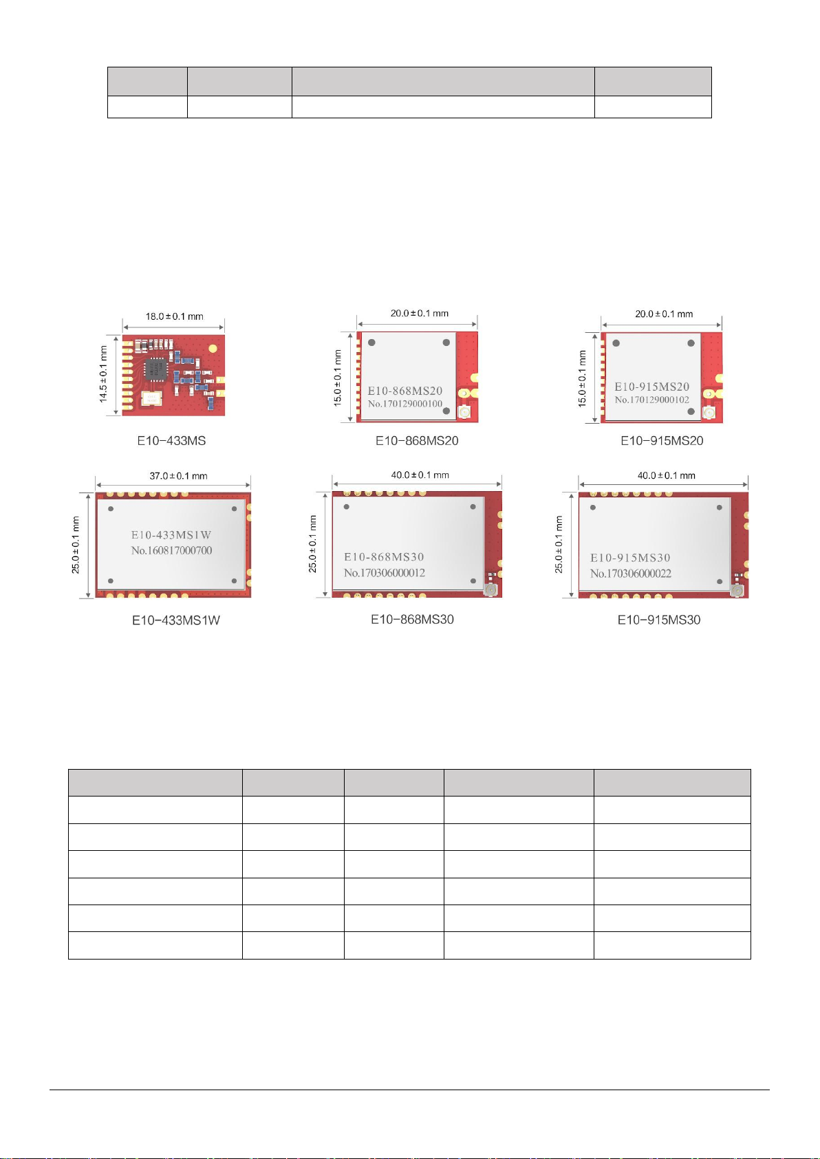
2.1. E10-433MS
2.2. E10-433MS1W
2.3. E10-868MS20/ E10-915MS20
2.4. E10-868MS30/ E10-915MS30
3. RECOMMENDED CIRCUIT DIAGRAM
3.1. E10-433MS/ E10-868MS20/E10-915MS20
3.2. E10-868MS30/ E10-915MS30
3.3. E10-433MS1W
4. NOTES
5. PRODUCTION GUIDANCE
5.1. REFLOW SOLDERING TEMPERATURE
5.2. REFLOW CURVING DIAGRAM
6. FAQ
6.1. COMMUNICATION RANGE IS TOO SHORT
6.2. MODULE IS EASY TO DAMAGE
............................................................................................................................................................................................
................................................................................................................................................................................................
.................................................................................................................................................................................
...........................................................................................................................................................................
.................................................................................................................................................
.................................................................................................................................................
......................................................................................................................................
...............................................................................................................................................
.........................................................................................................................................................................
..........................................................................................................................................................
..............................................................................................................................................
........................................................................................................................................................
.......................................................................................................................................
......................................................................................................................................................
..........................................................................................................................
6
7
8
9
10
10
10
11
11
12
12
12
13
13
13
7. IMPORTANT NOTES
8. ABOUT US
Copyright ©2012–2017,Chengdu Ebyte Electronic Technology Co.,Ltd.
2
.....................................................................................................................................................................................
....................................................................................................................................................................
13
13

SI4463 wireless module E10 series user manual
1. Technical Parameter
1.1. General Parameter
Model
Core IC
Size
Net Weight
Operating
Temperature
Operating
Humidity
Storage
Temperature
E10-433MS
SI4463
14.5 * 18.5 mm
0.8±0.1g
-40 ~ 85°C
10% ~ 90%
-40 ~ 125°C
E10-433MS1W
SI4463
25 * 37 mm
5.0±0.1g
-40 ~ 85°C
10% ~ 90%
-40 ~ 125°C
E10-868MS20
SI4463
15*20 mm
1.5±0.1g
-40 ~ 85°C
10% ~ 90%
-40 ~ 125°C
E10-868MS30
SI4463
25*40 mm
5.0±0.1g
-40 ~ 85°C
10% ~ 90%
-40 ~ 125°C
E10-915MS20
SI4463
15*20 mm
1.5±0.1g
-40 ~ 85°C
10% ~ 90%
-40 ~ 125°C
E10-915MS30
SI4463
25*40 mm
5.0±0.1g
-40 ~ 85°C
10% ~ 90%
-40 ~ 125°C
1.2. Electrical Parameter
1.2.1. Transmitting current
Model
Min
Typ
Max
Unit
Remarks
E10-433MS
76.4
83.0
91.3
mA
●When designing current supply circuit, 30% margin is recommended
to be remained so as to ensure long-term stable operation of the
whole module;
●The current at the instant of transmitting may be high, but the total
energy consumed may be lower due to very short transmitting time;
●When using external antenna, the impedance matching degree at
different frequency points between antenna and module may affect
the transmitting current value at different levels.
E10-433MS1W
607.2
660.0
726.0
mA
E10-868MS20
87.4
95.0
104.5
mA
E10-868MS30
672.5
731.0
804.1
mA
E10-915MS20
90.2
98.0
107.8
mA
E10-915MS30
692.8
753.0
828.3
mA
1.2.2. Receiving current
Model
Min
Typ
Max
Unit
Remarks
E10-433MS
14.7
16.0
17.6
mA
●The current consumed when the RF chip is only working at receiving
mode is called as receiving current,the tested receiving current may
be higher for some RF chips with communication protocol or the
developers have loaded their own protocol to the whole module;
● The current at pure receiving mode will be mA level, users can
realize µA level of receiving current through firmware development.
E10-433MS1W
20.2
22.0
24.2
mA
E10-868MS20
14.7
16.0
17.6
mA
E10-868MS30
18.4
20.0
22.0
mA
E10-915MS20
14.7
16.0
17.6
mA
E10-915MS30
18.4
20.022mA
1.2.3. Turn-off current
Model
Min
Typ
Max
Unit
Remarks
E10-433MS
0.3
0.6
2.1
µA
● The turn-off current means the current consumed by CPU, RAM,
Clock and some registers which remain operating. SoC is at very low
power consumption status;
● The turn-off current is always lower than the current consumed
when the power supply source of the whole module is at no-load
status.
E10-433MS1W
2.5
5.0
6.5
µA
E10-868MS20
0.2
0.4
1.9
µA
E10-868MS30
2.5
5.0
6.5
µA
E10-915MS20
0.2
0.4
1.9
µA
E10-915MS30
2.5
5.0
6.5
µA
Copyright ©2012–2017,Chengdu Ebyte Electronic Technology Co.,Ltd.
3

SI4463 wireless module E10 series user manual
1.2.4. Voltage supply
Model
Min
Typ
Max
Unit
Remarks
E10-433MS
1.8
3.3
3.6
V DC
●If the module stays at maximum voltage for a long time, it may be
damaged;
● The power supply pin has certain surge-resistance ability, but the
potential pulse is higher than the maximum power supply voltage;
●The power supply is not advisable to be below 3.0V, or the RF
parameters will be influenced at different degree.
● For max 30dBm, voltage is no less than 4.75V,or RF parameters
will be affected to different extend.
E10-433MS1W
4.8
5.0
5.5
V DC
E10-868MS20
1.8
3.3
3.6
V DC
E10-868MS30
4.8
5.0
5.5
V DC
E10-915MS20
1.8
3.3
3.6
V DC
E10-915MS30
4.8
5.0
5.5
V DC
1.2.5. Communication level
Model
Min
Typ
Max
Unit
Remarks
E10-433MS
1.8
3.3
3.6
V DC
● If the module stays at maximum communication level for a long
time, it may be damaged;
● There are various ways to switch communication level, but it will
affect the whole power consumption to a large extend.
E10-433MS1W
1.8
3.3
3.6
V DC
E10-868MS20
1.8
3.3
3.6
V DC
E10-868MS30
1.8
3.3
3.6
V DC
E10-915MS20
1.8
3.3
3.6
V DC
E10-915MS30
1.8
3.3
3.6
V DC
1.3. RF Parameter
1.3.1. Transmitting power
Model
Min
Typ
Max
Unit
Remarks
E10-433MS
19.6
20.0
20.5
dBm
● Due to the error of the materials, each LRC component has ± 0.1%
error, so error accumulation will occur since multiple LRC
components are used in the whole RF circuit, and the transmitting
currents will be different at different modules;
● The power consumption can be lowered by lowering the
transmitting power, but the efficiency of the internal PA will be
decreased by lowering transmitting power due to various reasons;
● The transmitting power will be lowered by lowering the power
supply voltage.
E10-433MS1W
29.6
30.0
30.5
dBm
E10-868MS20
19.6
20.0
20.5
dBm
E10-868MS30
29.6
30.0
30.5
dBm
E10-915MS20
19.6
20.0
20.5
dBm
E10-915MS30
29.6
30.0
30.5
dBm
1.3.2. Receiving Sensitivity
Model
Min
Typ
Max
Unit
Remarks
E10-433MS
-121.0
-122.0
-124.0
dBm
● The sensitivity is tested under the air data rate 1.3kbps;
● Due to the error of the materials, each LRC component has ± 0.1%
error, so error accumulation will occur since multiple LRC
components are used in the whole RF circuit, and the transmitting
currents will be different at different modules;
●The receiving sensitivity will be reduced and communication range
will be shortened while increasing the air data rate.
E10-433MS1W
-122.0
-123.0
-125.0
dBm
E10-868MS20
-121.0
-122.0
-124.0
dBm
E10-868MS30
-122.0
-123.0
-125.0
dBm
E10-915MS20
-121.0
-122.0
-124.0
dBm
E10-915MS30
-122.0
-123.0
-125.0
dBm
Copyright ©2012–2017,Chengdu Ebyte Electronic Technology Co.,Ltd.
4
 Loading...